International Journal of Emerging Technology and Advanced Engineering
Website: www.ijetae.com (ISSN 2250-2459,ISO 9001:2008 Certified Journal, Volume 4, Issue 5, May 2014)
88
Modeling and Simulation of SONOS with Optimized Layer
Thickness for Obtaining The Properties of Ideal Non-Volatile
Memories
Khyati Khanpal
1, Praneeta Malkani
2, Renu Nainwal
3,
Shivani Saxena
41,2,3M.tech VLSI design, Banasthali University 4
Department of electronics Banasthali University, Raj.
Abstract- This research investigated the scaling effects on different layers like tunneling layer, charge trapping layer and blocking layer on SONOS-type nonvolatile semiconductor memories and finally conclude a range of thickness for these layers. It is found that the scaling of layers have significant effect on data retention. We can’t scale down our device below a certain limit as this directly detoriates the characteristic of our device. In addition, which layer effect the function most, of SONOS, has also been seen.
Keywords-- Blocking layer, Charge trapping layer, Data retention, SONOS, Tunneling layer.
I. INTRODUCTION
SONOS (polysilicon-oxide-nitride-oxide-silicon) type nonvolatile semiconductor memories have been investigated as the replacement of conventional floating gate memories. This type of memories have several advantages over the conventional floating gate flash memories, such as lower operating voltage, excellent endurance and compatibility with standard complementary metal-oxide-semiconductor (CMOS) technology. However, their operating speed and date retention characteristics are still the bottlenecks to limit the applications of SONOS memories. Recently, various approaches have been used to make a trade-off between the operating speed and the data retention characteristics.
[image:1.612.318.573.272.458.2]Application of high-k dielectrics (HfO2, Ta2O5, Al2O3, Y2O3, ZrO2 to SONOS-type memories is a predominant route.
Table I
Comparison In Between Different Non-Volatile Memories [1]
S.No. Parameters
SNOS NV-SRAM MNOS EE- PROM SONOS EE-PROM
1. Speed
(access time)
35 nsec 150 nsec 150
nsec 2. write time 35 nsec Byte 10 msec
Byte
10 msec Byte 3. endurance power cycle write Cycle write cycle
4. radiation
hardness
high low high
5. Cost moderate low moderate
6. limitation density write speed write
speed
II. SONOS
SONOS non-volatile memory devices are fabricated with an ONO gate dielectric consisting of a tunnel oxide, “oxy-nitride” layer, and a „blocking‟ oxide underneath a phosphorus-doped polysilicon gate, as shown in fig I. The device is programmed by applying voltage to the gate terminal and erased by applying erase voltage to the device. The applied voltage attracts electrons or holes to the surface of the silicon depending on the polarity of the gate voltage . Carriers „tunnel‟ through an ultra-thin oxide and are stored in “traps” in the oxy-nitride layer. [1]
[image:1.612.363.520.591.683.2]International Journal of Emerging Technology and Advanced Engineering
Website: www.ijetae.com (ISSN 2250-2459,ISO 9001:2008 Certified Journal, Volume 4, Issue 5, May 2014)
89
III. PROPERTIES OF DIFFERENT LAYERS IN SONOS
A. Tunneling layer
This layer tunnels the charge carriers from substrate into charge-trapping layer. Speed and data retention are affected by tunneling layer. In the SONOS devices, thin silicon dioxide is typically used as the tunneling layer, since it has high operating speed, low write/erase voltage and superior endurance.
B. Charge trapping layer
This layer contains charge trap centers able to hold an electrostatic charge. Charge trapping layer must have high trap density. traps are considered to originate from defects, which capture electrons or holes. However, only a certain traps can store charges and maintain a stable memory characteristic after programming, which are considered as effective traps for memory application.
C. Blocking layer
This layer prevents tunneling of charge carriers into gate. It should have high barrier height and feasible permittivity.
D. Conventional materials used in SONOS
Tunneling Layer- SiO2
Charge Trapping Layer- Si3N4 Blocking Layer- SiO2
Fig II: Different layers of SONOS [3]
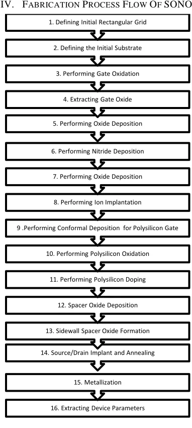
IV. FABRICATION PROCESS FLOW OF SONOS
[image:2.612.345.536.137.561.2]Fig III: Process flow in Athena
A. Defining Initial Rectangular Grid
Defining the initial rectangular grid is critical in process simulation. The number of nodes in the grid has a direct influence on simulation accuracy and time. A finer grid should exist in those areas of the simulation structure where active device should formed.
16. Extracting Device Parameters 15. Metallization 14. Source/Drain Implant and Annealing
13. Sidewall Spacer Oxide Formation 12. Spacer Oxide Deposition 11. Performing Polysilicon Doping 10. Performing Polysilicon Oxidation 9 .Performing Conformal Deposition for Polysilicon Gate
8. Performing Ion Implantation 7. Performing Oxide Deposition 6. Performing Nitride Deposition
International Journal of Emerging Technology and Advanced Engineering
Website: www.ijetae.com (ISSN 2250-2459,ISO 9001:2008 Certified Journal, Volume 4, Issue 5, May 2014)
90
B. Defining the Initial Substrate
Initial substrate initialize the material and orientation, concentration-field, dimensionality of simulation structure.
C. Performing Gate Oxidation
An oxide layer is deposited on the substrate material using dry oxidation by diffusion process.
D. Extracting Gate Oxide Thickness
Extracting is done to combine and manipulate values or entire curves quickly and easily. We have to extract the gate oxide thickness that was grown during the oxidation process step.
E. Performing Oxide Deposition
Oxide deposition is done to form tunneling layer by dry oxidation process. Oxide layer is deposited over the gate region of the simulation structure.
F. Performing Nitride Deposition
Nitride layer is used as charge trapping layer in simulation structure. This layer is formed by LPCVD process.
G. Performing Oxide Deposition
This oxide layer act as blocking layer in simulation structure and formed by LPCVD process.
H. Performing Ion Implantation
Ion implantation is used to introduce doping impurities into semiconductor device structures. Ion implantation is performed by implant process.
I. Performing Conformal Deposition for Polysilicon Gate
Conformal deposition for polysilicon is used to generate multilayered structures, when exact shape of deposit layer is not critical.
J. Performing Polysilicon Oxidation
Polysilicon oxidation is done prior to doping of the polysilicon by ion-implantation. The recipe used for polysilicon oxidation is wet oxidation.
K. Performing Polysilicon Doping
Polysilicon doping is performed to introduce the impurities that provide the desired properties the gate.
L. Spacer Oxide Deposition
Spacer oxide deposition has to be performed prior to the source and drain implants.
M. Sidewall Spacer Oxide Formation
Sidewall oxide spacer is performed by dry etch step.
N. Source/Drain Implant and Annealing
To form the source/drain of the simulation structure an implantation will be performed. The source/drain implant is then followed by a short annealing process.
O. Metallization
Metallization attributes an electrode to any metal, or polysilicon region. It is done by depositng the electrode material.
P. Extracting Device Parameters
Device parameters as, junction depth, source/drain sheet resistance, LDD sheet resistance under oxide spacer and the long channel threshold voltage are extracted by extract process.
V. MODELING AND SIMULATION PARAMETERS OF SONOS
1. Grid Specification: 0.6um x 1um 2. Tunneling Layer:
Material – SiO2
Thickness – 0.002um 3. Charge Trapping Layer: Material- Si3N4
Thickness- 0.0045um 4. Blocking Layer: Material- SiO2 Thickness – 0.0055um 5. Electrode: Source, Gate, Drain 6. Methods
:
SRH / Consrh, Fermi-Dirac / Boltzmann
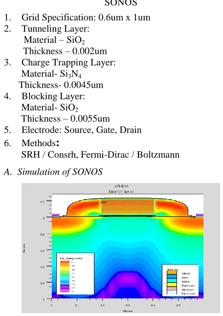
[image:3.612.320.548.365.688.2]A. Simulation of SONOS
International Journal of Emerging Technology and Advanced Engineering
Website: www.ijetae.com (ISSN 2250-2459,ISO 9001:2008 Certified Journal, Volume 4, Issue 5, May 2014)
91
The above figure shows different layers of silicon, SiO2, Si3N4 , Polysilicon, Aluminum and electrode.
B. SONOS stack
[image:4.612.64.273.175.344.2].
Fig V: Oxide nitride oxide stack with thickness 0.002um/0.0045um/0.0055um.
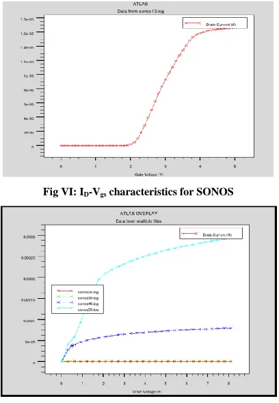
C. Id – Vgs Characteristics for SONOS
[image:4.612.339.546.218.378.2]The curve in fig VI, shown drain current is constant initially after it increases with the increase in gate to source voltage and at last current comes in saturation.
[image:4.612.67.271.410.704.2]Fig VI: ID-Vgs characteristics for SONOS
Fig VII: ID- VDS Characteristics for SONOS
Figure shows that drain current increases with increasing drain voltage, become constant when saturation occurs, at constant gate voltage.
D. Write and Erase Operation
For charging, apply positive voltage on gate terminal and for erasing, apply negative voltage on gate terminal.
Fig VIII : Charging and Erase Operation for SONOS(ideal)
This graph shows Ideal characteristics of erasing and charging operation taken by Silvaco, where red and blue line shows before charging and erasing respectively. Green line shows after charging. (in every case discuss below)
VI. SCALING OF SONOS
1. Tunneling layer=3.2nm, charge trapping layer=5nm, blocking layer=10nm
The figure above shows scaling of tunneling layer from 4nm to 3.3 nm, after charging characteristic drops, which signifies data retention decreases.
[image:4.612.327.560.463.628.2]International Journal of Emerging Technology and Advanced Engineering
Website: www.ijetae.com (ISSN 2250-2459,ISO 9001:2008 Certified Journal, Volume 4, Issue 5, May 2014)
92
The figure above shows scaling of tunneling layer from 2.8nm to 1.1nm, after charging characteristic drops further, which signifies more decrement in data retention.
3. Tunneling layer=1nm, charge trapping layer=5nm, blocking layer=10nm
The figure above shows scaling of tunneling layer from 1.1nm to 1nm, after charging characteristic signifies zero data retention.
4. Tunneling layer=4nm, charge trapping layer=5nm, blocking layer=6nm
The figure above shows scaling of blocking layer from 10 nm to 6nm, after charging characteristic drops. This shows scaling of blocking layer has significant impact on data retention behavior.
5. Tunneling layer=4nm, charge trapping layer=5nm, blocking layer=1nm
The figure above shows scaling of blocking layer upto 1nm, after charging characteristic and erasing characteristic coincides.
6. Tunneling layer=4nm, charge trapping layer=2nm, blocking layer=6nm
The figure above shows scaling of charge trapping from 4nm to 2nm, after charging characteristic has significant decrease.
VII. CONCLUSION AND VALIDATION
The above result interpretate the range of different layers:
International Journal of Emerging Technology and Advanced Engineering
Website: www.ijetae.com (ISSN 2250-2459,ISO 9001:2008 Certified Journal, Volume 4, Issue 5, May 2014)
93
If the range of different layers decreases further, data retention, turn-on time, programming voltage and write/erase time will be effected. As Thickness of tunneling layer decreases, programming voltage must be reduced to maintain a constant electric field and programming speed. Write/ erase speed increases due to scaling however, memory loss for the erase state increases due to back tunneling. Thus, there is a tradeoff between the erase/write speed and memory retention in scaled SONOS device structures. The reduction in memory retention is manifested by scaling of charge trapping layer. By decrease in the blocking oxide thickness turn-on time is reduced[4]. The results of [4] demonstrate that the fabricated devices can be programmed as fast as 1 s and erased from 10 ns at an 8-V gate bias.
The retention decay rate of this device is improved by a factor more than three as compared to the conventional MONOS/SONOS type devices. Our result is very close to this result.
REFERENCES
[1] Bob Peters, Defense Electronics, p.82, (1991). [2] Chen P.C.Y. (1977) IEEE Tr. O E.D.,ED 24,584.
[3] Khyati Kandpal, Praneeta Malkani, Renu Nainwal, Shivani Saxena, ” A Review of Evolution comes in Non Volatile Semiconductor memories like SONOS with the role of high k-dielectric material,” IOSR Journal of Engineering (IOSRJEN), Vol. 04, Issue 01, January 2014. pp- 13-17.
![Table I Comparison In Between Different Non-Volatile Memories [1]](https://thumb-us.123doks.com/thumbv2/123dok_us/8714683.882753/1.612.363.520.591.683/table-i-comparison-different-non-volatile-memories.webp)