An Improved SOI CMOS Technology Based Circuit
Technique for Effective Reduction of
Standby Subthreshold Leakage
Manish Kumar1, Md. Anwar Hussain1, Sajal K. Paul2
1Department of Electronics and Communication Engineering, North Eastern Regional Institute of Science
and Technology, Arunachal Pradesh, India
2Department of Electronics Engineering, Indian School of Mines, Jharkhand, India
Email: [email protected], [email protected], [email protected]
Received August 18, 2013; revised September 18, 2013; accepted September 25,2013
Copyright © 2013 Manish Kumar et al. This is an open access article distributed under the Creative Commons Attribution License, which permits unrestricted use, distribution, and reproduction in any medium, provided the original work is properly cited.
ABSTRACT
Silicon-on-insulator (SOI) CMOS technology is a very attractive option for implementing digital integrated circuits for low power applications. This paper presents migration of standby subthreshold leakage control technique from a bulk CMOS to SOI CMOS technology. An improved SOI CMOS technology based circuit technique for effective reduction of standby subthreshold leakage power dissipation is proposed in this paper. The proposed technique is validated through design and simulation of a one-bit full adder circuit at a temperature of 27˚C, supply voltage, VDD of 0.90 V in 120 nm SOI CMOS technology. Existing standby subthreshold leakage control techniques in CMOS bulk technology are compared with the proposed technique in SOI CMOS technology. Both the proposed and existing techniques are also implemented in SOI CMOS technology and compared. Reduction in standby subthreshold leakage power dissipa- tion by reduction factors of 54x and 45x foraone-bit full adder circuit was achieved using our proposed SOI CMOS technology based circuit technique in comparison with existing techniques such as MTCMOS technique and SCCMOS technique respectively in CMOS bulk technology. Dynamic power dissipation was also reduced significantly by using this proposed SOI CMOS technology based circuit technique. Standby subthreshold leakage power dissipation and dy- namic power dissipation were also reduced significantly using the proposed circuit technique in comparison with other existing techniques, when all circuit techniques were implemented in SOI CMOS technology. All simulations were per- formed using Microwindver 3.1 EDA tool.
Keywords: Standby Subthreshold Leakage; SOI Technology; Low Power; Multi-Threshold Voltage; Stack
Effect; Reverse Gate Voltage
1. Introduction
In recent years, the demand for reducing the standby sub- threshold leakage power has grown significantly. This tremendous demand is mainly due to the fast growth of battery-operated portable applications such as notebook and laptop computers, personal digital assistants, cellu- lar phones, and other portable communication devices, which remain in the standby state for a significant time interval. This leakage power dissipation is mainly no- ticeable in electronic portable battery operated systems having burst-mode type integrated circuits, where com- putation occurs for only short intervals and the system spends the majority of time in standby state [1]. Reduc- tion of this subthreshold leakage power is highly desir- able for battery operated portable systems, which remain in
and the transistor has reached the steady state. Excessive standby subthreshold leakage power dissipation is a pri- mary hindrance for the advancement of CMOS integrated circuits with further scaling down in technology. Sup- pressing subthreshold leakage current in integrated cir- cuits is essential for achieving green computing and fa- cilitating the proliferation of portable electronic devices. This leakage power is expected to increase 32 times per device by the year 2020 [4]. CMOS logic circuit having submicron MOSFETS involves a number of complex tradeoffs in device dimensions, which supply voltage, and the threshold voltage for minimizing this subthresh- old leakage power dissipation.
Today most electronic circuits are realized using a bulk CMOS technology, which is a very mature techno- logy. Both die size and power dissipation of electronic circuits using this bulk CMOS technology will become difficult to reduce in the future [5]. So, new advanced technologies have to be developed for reducing these emerging problems. The most promising one for ultra- low power circuit implementation is silicon-on-insulator (SOI) CMOS technology [5-7]. The ability to use a low supply voltage and to simultaneously reduce parasitic capacitances is of high importance in designing low po- wer digital circuits [8]. Instead of a bulk silicon substrate, SOI CMOS technology employs an insulator below a thin layer of silicon which eliminates most of the para- sitic capacitances found in bulk CMOS technology. This allows SOI CMOS circuits to operate with a reduced supply voltage, thus further reducing the system power consumption.
Short channel effects (SCE) such as short channel threshold voltage roll off and drain induced barrier low- ering (DIBL) are becoming major challenges in deep submicron MOS transistors and circuits in CMOS tech- nology. In order to minimize SCE, advanced MOSFET technologies have to be used. Short channel effects of MOSFETs are much less in silicon-on-insulation (SOI) technology in comparison with conventional CMOS bulk technology [9]. The main advantage of SOI technology is its reduced junction capacitance due to oxide isolation of individual circuit elements, resulting in the overall lower power dissipation. Silicon-on-insulator (SOI) technology has attracted considerable attention as a potential alterna- tive substrate for low power application. The use of sili- con-on-insulator (SOI) technology is bringing new pos- sibilities for effective reduction of the standby sub- threshold leakage power dissipation. However, the main drawback with SOI CMOS technology is its high manu- facturing cost which can be prohibitive for products where low system cost is of primary concern.
Techniques such as multi-threshold CMOS (MTCM- OS) technique [10,11], and super cutoff CMOS (SCCM- OS) technique [12] are available in the literature for the
reduction of standby subthreshold leakage power in CMOS bulk technology. In MTCMOS technique, the high VTH MOS transistor can limit the down scaling of the supply voltage, VDD for ultra-low power applications due to the increase in the circuit delay. The delay is in- fluenced by the reduced effective supply voltage and use of high VTH MOS transistors. The main advantage of SCCMOS technique over MTCMOS technique is the reduction in the circuit delay due to the use of low VTH sleep MOS transistors. However, in SCCMOS technique, a complex controller circuit is used for providing both negative and positive gate voltages, VGS to completely turn off nMOS and pMOS transistors respectively.
In this paper, an improved SOI CMOS technology based circuit technique is proposed for effective reduc- tion of the subthreshold leakage power dissipation in standby mode. To compare the proposed technique in SOI CMOS technology with existing (MTCMOS and SCCMOS) standby subthreshold leakage control tech- niques in CMOS bulk technology, a one-bit full adder circuit is designed and simulated using the proposed technique. The proposed and existing techniques are also implemented in SOI CMOS technology and compared. The proposed circuit technique in SOI CMOS technology is found to dissipate the least standby subthreshold leak- age power and also dynamic power dissipation is reduced significantly in comparison with other existing circuit techniques in CMOS bulk technology. Standby sub- threshold leakage power dissipation and dynamic power dissipation are also reduced significantly using the pro- posed circuit technique in comparison with other existing techniques, when all circuit techniques are implemented in SOI CMOS technology.
The rest of the paper is organized as follows: Section 2 describes about the fundamentals and advantages of sili- con-on-insulator technology for low power applications over bulk CMOS technology. Section 3 describes the subthreshold leakage power dissipation model in more details. In Section 4, a methodology for reducing the subthreshold leakage power dissipation in standby mode is discussed. Section 5 describes the proposed SOI CMOS technology based circuit technique for effective reduction of the standby subthreshold leakage power dis- sipation. In Section 6, simulation results are provided for a one-bit full adder circuit and the obtained results are compared using the existing circuit techniques in CMOS bulk technology and the proposed SOI CMOS technol- ogy based circuit technique. Finally, conclusion is pro- vided in Section 7.
2. Silicon-on-Insulator CMOS Technology
manufacturing. Instead of using silicon as the substrate, as in bulk CMOS transistors, an insulating substrate can be used to improve device characteristics [13]. SOI CMOS circuits consist of single-device islands which are dielectrically isolated from each other and also from the underlying substrate. Since there are virtually no isola- tion constraints for individual devices, transistor and in- terconnect densities can be very high. In bulk CMOS devices every junction produces undesirable parasitic ca- pacitances as well. These junction capacitances do exist in SOI CMOS devices also, but they are reduced by a factor ranging from 4 to 7 [14,15]. The main advantage of SOI technology is its reduced junction capacitance, resulting in the overall lower power dissipation.
3. Subthreshold Leakage Power Dissipation
Model
Subthreshold leakage current occurs in a MOS transistor when the gate voltage, VGS is below the threshold voltage of the MOS transistor. BSIM 4 subthreshold leakage cur- rent model [16] can be expressed as:
GS THO DS BS DS
T T
–
SUB e 1 e
V V V V V
nV V
O
I I
(1)
2 1.8
0 OX Te and T
W KT
I C V V
L q
(2)
where VGS, VDS and VBS are the gate to source, drain to source, and bulk to source voltages respectively, μ de- notes the carrier mobility, Cox is the gate oxide capaci- tance per unit area, W and L denote the channel width and channel length of the leaking MOS transistor respec- tively, K is the Boltzmann constant, T is the absolute temperature, q is the electrical charge of an electron, VT is the thermal voltage, VTHO is the zero biased threshold voltage, γ is body effect coefficient, η denotes the drain induced barrier lowering coefficient, and n is the sub- threshold swing coefficient.
In a logic circuit, the subthreshold leakage power dis- sipation can be calculated as the product of the number of nMOS and pMOS transistors (NnMOS & NpMOS), the average subthreshold leakage current per MOS transistor (ISUBAVG.), and the supply voltage, VDD. Hence it may be expressed as:
SUB nMOS pMOS SUBAVG DD
P N N I V (3) where ISUBAVG. is calculated by computing the average leak- age current per MOS transistor for the given logic circuit using gate-level subthreshold leakage power estimation.
4. Methodology Adopted
Methodology for designing the proposed technique for effective reduction of the standby subthreshold leakage power is adopted after careful investigation of the sub-
threshold leakage current equations described in section 3.
[image:3.595.86.284.343.410.2]Gate voltage, VGS can be lowered by utilizing the prin- ciple of reverse gate voltage, VGS to MOS transistors. There is an exponential decrease in the standby sub- threshold leakage current due to the application of posi- tive and negative gate voltages to pMOS and nMOS transistors respectively [16,17]. So, subthreshold leakage power dissipation can be reduced effectively by applying reverse gate voltages to MOS transistors.
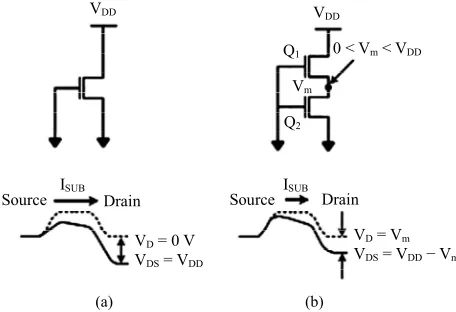
Figure 1 [18] shows the reduction of the subthresh-
old leakage current due to the increase in the barrier height and the reduction in VDS (= VDD – Vm) after stack- ing of two cutoff nMOS transistors in comparison with a single cutoff nMOS transistor. When both nMOS tran- sistors, Q1 and Q2 are turned off due to the application of
VGS < VTH, then the intermediate node voltage, Vm has a positive value due to the existence of a small drain cur- rent. Thus, the gate to source voltage of Q1 is negative, due to which the subthreshold leakage current reduces exponentially. The body effect of Q1 (due to Vm > 0), further increases VTH of Q1, thereby, reduces the sub- threshold leakage current. Drain induced barrier lowering (DIBL) is also reduced due to the positive value of node voltage, Vm. This increases VTH of Q2, which also con- tributes to the reduction of the subthreshold leakage cur- rent. Thus, the subthreshold leakage current is reduced considerably, due to stacking effect of MOS transistors.
Threshold voltage of a MOS transistor plays a vital role in low power VLSI circuit design. In the active mode of circuit operation, low VTH MOS transistors are preferred for higher performance. However, for the standby mode of circuit operation, high VTH MOS tran- sistors are used for reducing the subthreshold leakage power dissipation. Hence, MTCMOS circuit technique- can be utilized for effectively reducing the standby sub- threshold leakage power dissipation.
VDD
VD = Vm
VDS = VDD− Vm
Drain ISUB
Source
Q1
Q2
0 < Vm < VDD
VDD
ISUB
Drain Source
VD = 0 V
VDS = VDD
Vm
(a) (b)
[image:3.595.308.536.544.700.2]Silicon-on-insulator (SOI) is a non-bulk CMOS tech- nology. The reduction in the effective parasitic capaci- tance in SOI technology due to isolation from the bulk silicon makes it attractive for ultra-low power applica- tions. The dynamic power dissipation is proportional to the total circuit capacitance and the square of the supply voltage. This means that SOI technology is very much suitable for low power operations as the parasitic capaci- tance is reduced and the supply voltage can be lowered. A steeper subthreshold swing helps to achieve low sub- threshold leakage power dissipation.
The subthreshold swing S of a MOS transistor can be expressed as [19]:
d
ox
ln10 1 C KT
S
q C
(4) where K is the Boltzmann constant, T is the absolute temperature, q is the elementary charge, and Cd and Cox are the capacitance of the depletion layer and gate oxide.
In SOI technology, Cd/Cox is close to zero as the deple- tion capacitance is negligible. An important feature in SOI technology is the steeper sub threshold slope due to a reduction in the substrate body effect. For a given Ioff-current, the SOI technology has a much smaller threshold voltage, which means that the circuit can operate at a lower sup- ply voltage. SOI technology has lower DIBL, lesser short channel effects, very good subthreshold swing, and lesser junction and parasitic capacitances in comparison with the bulk CMOS technology. Thus, the subthreshold leakage current in SOI technology is much lower than the bulk CMOS technology for the same threshold vol- tage.
5. Proposed Circuit Technique
The proposed circuit technique is designed after analyz- ing the dependence of MOS transistor parameters on the subthreshold leakage current. Methodology adopted for designing this SOI based circuit technique is discussed in detail in Section 4.
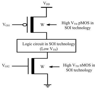
Figure 2 show salogic circuit designed using MTCM-
OS technique in SOI CMOS technology. This logic cir- cuit is designed using low VTH MOS transistors, and a high VTHpMOS transistor is inserted between the supply voltage, VDD and the logic circuit while a high VTHnMOS transistor is inserted between the logic circuit and the ground. During standby mode of operation, VGS1 is con- nected to a positive gate voltage, while VGS2 is connected to the ground as per MTCMOS technique. Figure 3
shows a logic circuit using the proposed SOI CMOS technology based circuit technique, which is designed from Figure 2 after stacking high VTH MOS transistors
and applying reverse gate voltages, VGS1 and VGS2 (i.e. positive gate voltage, VGS1 to the stacked high VTHpMOS
High VTH pMOS in
SOI technology
High VTH nMOS in
SOI technology Logic circuit in SOI technology
(Low VTH)
W
VGS2
VGS1
VDD
[image:4.595.329.512.84.254.2]W
Figure 2. A logic circuit using MTCMOS techniquein SOI CMOS technology.
Logic circuit SOI technology
(Low VTH)
Stacking of High VTH nMOS
in SOI technology W/2
W/2
VGS2
VGS1
W/2
W/2
Stacking of High VTH pMOS
in SOI technology
[image:4.595.325.524.294.489.2]VDD
Figure 3. A logic circuit using the proposed circuit techni- que in SOI technology.
transistors and negative gate voltage, VGS2 to the stacked high VTHnMOS transistors) to the stacked high VTHpMOS and nMOS transistors respectively in SOI CMOS tech-nology.
In this proposed technique, standby subthreshold leak- age current is reduced effectively by utilizing multi-thre- shold MOS transistors, stacking of MOS transistors, ap- plying reverse gate voltages, VGS1 and VGS2 (positive gate voltage, VGS1 to the stacked high VTHpMOS transistors and negative gate voltage, VGS2 to the stacked high VTH- nMOS transistors) to MOS transistors, and using silicon- on-insulator (SOI) CMOS technology.
6. Simulation Results and Observations
Figure 4 shows the circuit diagram of a one-bit full ad-
GND VGS2
SUM VDD
VGS1
A
B
C
[image:5.595.56.286.88.239.2]CARRY
Figure 4. Circuit diagram of a one-bit full adder using the proposed technique in SOI CMOS technology.
ogy is compared with the existing techniques in CMOS bulk technology in terms of standby subthreshold leakage power dissipation, and also dynamic power dissipation. Layout of a one-bit full adder circuit was designed and simulated using Microwind ver. 3.1 EDA tool. All simu- lations were performed at a temperature of 27˚C and supply voltage, VDD of 0.9 V in 120 nm SOI CMOS and bulk CMOS technologies. W/L of low VTHnMOS and pMOS transistors were taken as 0.72 μm/0.12 μm and 1.20 μm/0.12 μm respectively. Similarly, W/L of high
VTHnMOS and pMOS transistors were taken as 0.72 μm/ 0.24 μm and 1.20 μm/0.24 μm respectively.
Standby subthreshold leakage power dissipation was measured by combining all possible input vector combi- nations. For calculation of standby subthreshold leakage power dissipation in a logic circuit, the voltage magni- tude of all input vectors should always be less than the magnitude of the threshold voltage of the MOS transistor of the logic circuit. In this proposed technique, sub- threshold leakage power dissipation in standby mode for a one bit full adder was calculated by connecting reverse gate voltages, VGS1 and VGS2 (positive gate voltage, VGS1 to stacked high VTHpMOS transistors and negative gate voltage, VGS2 to stacked high VTHnMOS transistors) to high VTH stacked MOS transistors and applying all com- binations of static input voltages, Vin < VTH to the logic circuit. Dynamic power dissipation using this proposed technique was calculated by applying input clock signals at a frequency of 5 GHz.
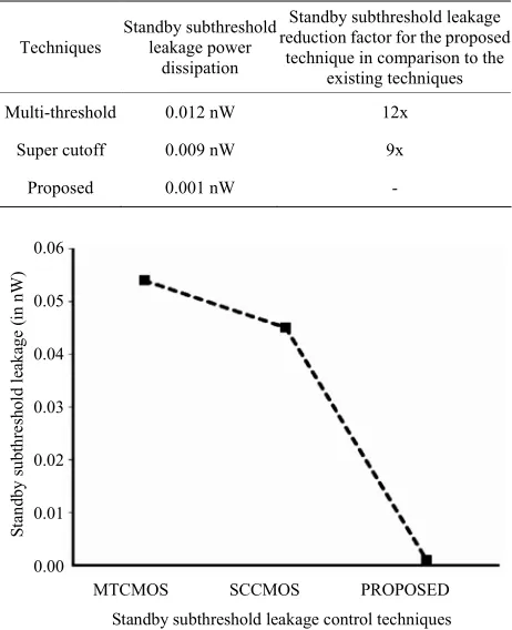
Standby subthreshold leakage power dissipation and standby subthreshold leakage reduction factor for a one- bit full adder circuit using the proposed technique in SOI CMOS technology in comparison with existing tech- niques in CMOS bulk technology are shown in Tables 1
and 2 respectively. Figures 5 and 6 are the graphical
representations of Tables 1 and 2 for standby subthresh-
old leakage power and standby subthreshold leakage re- duction factor respectively. Similarly Figures 7 and 8 are
Table 1. Standby subthreshold leakage power dissipation and dynamic power dissipation for a one-bit full adder cir- cuit using the proposed technique in SOI CMOS technology and existing techniques in CMOS bulk technology.
References Techniques leakage power dissipation Standby subthreshold Dynamic power dissipation
[10,11] MTCMOS 0.054 nW 0.050 μW
[12] SCCMOS 0.045 nW 0.041 μW
[image:5.595.309.537.133.211.2]Proposed Proposed 0.001 nW 0.012 μW
Table 2. Standby subthreshold leakage reduction factor and dynamic power dissipation reduction factor using the pro- posed technique in SOI CMOS technology in comparison with other existing techniques in CMOS bulk technology.
Techniques
Standby subthreshold leakage power
dissipation
Standby subthreshold leakage reduction factor for the proposed
technique in comparison to the existing techniques
Multi-threshold 0.012 nW 12x
Super cutoff 0.009 nW 9x
Proposed 0.001 nW -
0.06
0.05
0.04
0.03
0.02
0.01
0.00
St
an
dby
s
ubth
re
shol
d l
eak
ag
e
(i
n
nW
)
MTCMOS SCCMOS PROPOSED Standby subthreshold leakage control techniques
Figure 5. Standby subthreshold leakage power dissipation for a one-bit full adder circuit in MTCMOS, SCCMOS and proposed techniques.
the graphical representations of Tables 1 and 2 for dy-
namic power dissipation and dynamic power reduction factor respectively. Table 3 shows standby subthreshold
leakage power dissipation and standby subthreshold leak- age reduction factor for a one-bit full adder circuit, when both the proposed and existing circuit techniques are implemented in SOI CMOS technology. Table 4 shows
[image:5.595.308.539.271.555.2]56x
54x
52x
50x
48x
46x
44x
42x
40x
St
an
dby
s
ubth
re
shol
d l
eak
ag
e r
edu
ct
io
n f
act
or
[image:6.595.59.288.73.269.2]MTCMOS SCCMOS Standby subthreshold leakage control techniques
Figure 6. Standby subthreshold leakage reduction factor of the proposed technique in comparison to MTCMOS and SCCMOS techniques for a one-bit full adder circuit.
0.06
0.05
0.04
0.03
0.02
0.01
0.00
D
yna
m
ic
p
ow
er di
ss
io
at
ion
(in
n
W
)
[image:6.595.308.538.129.428.2]MTCMOS SCCMOS PROPOSED Standby subthreshold leakage control techniques
Figure 7. Dynamic power dissipation for a one-bit full ad- der circuit in MTCMOS, SCCMOS and proposed tech- niques.
Table 3. Standby subthreshold leakage power dissipation and standby subthreshold leakage reduction factor for a one-bit full adder circuit when both the existing techniques and the proposed technique are implemented in SOI CMOS technology.
Techniques Dynamic power dissipation
Dynamic power dissipation reduction factor for the proposed
technique in comparison with
existing techniques
Multi-Threshold 0.037 μW 3.083x
Super Cutoff 0.031 μW 2.583x
Proposed 0.012 μW -
[image:6.595.58.288.320.507.2]Reduction in the standby subthreshold leakage power
Table 4. Dynamic power dissipation and dynamic power reduction factor for a one-bit full adder circuit using both the existing techniques and the proposed technique in SOI CMOS technology.
Standby subthreshold leakage reduction factor using the proposed technique in SOI CMOS technology in comparison
with existing techniques in CMOS bulk technology
Dynamic power dissipation reduction factor using the proposed
technique in SOI CMOS technology in comparison with
existing techniques in CMOS bulk technology MTCMOS
technique
SCCMOS technique
MTCMOS technique
SCCMOS technique
54x 45x 4.167x 3.417x
4.5x
4.0x
3.5x
3.0x
2.5x
2.0x
1.5x
1.0x
0.0x
D
yn
am
ic pow
er
r
edu
ct
io
n
fa
ct
or
MTCMOS SCCMOS Standby subthreshold leakage control techniques
Figure 8. Dynamic power reduction factor of the proposed technique in comparison to MTCMOS and SCCMOS tech- niques for a one-bit full adder circuit.
dissipation by reduction factors of 54x and 45x foraone- bit full adder circuit is achieved using the proposed SOI CMOS based circuit technique in comparison to the ex- isting MTCMOS and SCCMOS techniques respectively in CMOS bulk technology. Dynamic power dissipation is also reduced significantly by reduction factors of 4.167x and 3.417x using the proposed SOI CMOS technology based circuit technique in comparison with MTCMOS and SCCMOS techniques respectively in CMOS bulk technology. It is also observed from Tables 3 and 4 that
the standby subthreshold leakage power dissipation and dynamic power dissipation are also reduced significantly using the proposed circuit technique in comparison with other existing techniques, when all circuit techniques are implemented in SOI CMOS technology.
7. Conclusion
[image:6.595.59.290.621.713.2]of standby subthreshold leakage power dissipation is presented in this paper. The proposed technique is vali- dated through layout design and simulation of a one-bit full adder circuit using the proposed and other existing standby subthreshold leakage control techniques. The proposed SOI CMOS technology based circuit technique dissipated the least standby subthreshold leakage power in comparison to other existing techniques in CMOS bulk technology. Dynamic power dissipation is also re- duced using this proposed technique in SOI technology in comparison with other presented techniques in CMOS bulk technology. It also reveals that when both the pro- posed and existing techniques are implemented in SOI CMOS technology, the proposed technique maintains the trend of reduced power dissipation in both standby and dynamic modes. Hence it may be concluded that the proposed SOI CMOS technology based circuit technique showed a significant improvement in the standby sub- threshold leakage power dissipation, which makes it at- tractive for ultra low-power applications.
8. Acknowledgements
This research work was partially supported by the Indian National Science Academy, New Delhi through INSA- visiting fellowship programme for the year 2012-13 vide number SP/VF-21/2012-13/306.
REFERENCES
[1] M. Anis and M. Elmasry, “Multi-Threshold CMOS Digi- tal Circuits: Managing Leakage Power,” Kluwer Aca-demic Publishers, Norwell, 2010.
[2] R. X. Gu and M. I. Elmasry, “Power Dissipation Analysis and Optimization of Deep Submicron CMOS Digital Circuits,” IEEE Journal of Solid-State Circuits, Vol. 31, No. 5, 1996, pp. 707-713.
[3] N. S. Kim, et al., “Leakage Current: Moore’s Law Meets Static Power,” IEEE Computer, Vol. 36, No. 12, 2003, pp.
68-75.
[4] S. Borkar, “Design Challenges of Technology Scaling,” IEEE Micro, Vol. 19, No. 4, 1999, pp. 23-29.
[5] Y. Kado, “The Potential of Ultrathin-Film SOI Devices for Low-Power and High-Speed Applications,” IEICE Transactions on Electronics, Vol. E80-C, No. 3, 1997, pp. 443-454.
[6] S. Cristoloveanu and G. Reichert, “Recent Advances in SOI Materials and Device Technologies for High Tem- perature,” Proceedings of High-Temperature Electronic
Materials, Devices and Sensors, San Diego, 22-27 Feb- ruary 1998, pp. 86-93.
[7] R. Reedy, et al., “Single Chip Wireless Systems Using SOI,” Proceedings of the International SOI Conference, San Diego, 4-7 October 1999, pp. 8-11.
[8] T. Iwamatsu, et al., “Analysis of the Delay Distributions of 0.5 μm SOI LSIs,” IEICE Transactions on Electronics, Vol. E80-C, No. 3, 1997, pp. 464-471.
[9] R. Yan, A. Ourmazd and K. F. Lee, “Scaling the Si MOSFET: From Bulk to SOI to Bulk,” IEEE Transac- tions on Electron Devices, Vol. 39, No. 7, 1992, pp. 1704-
1710.
[10] S. Mutoh, et al., “1-V Power Supply High—Speed Digi- tal Circuit Technology with Multi-Threshold Voltage CMOS,” IEEE Journal of Solid-State Circuits, Vol. 30, No. 8,
1995, pp. 847-854.
[11] M. Anis, S. Areibi and M. Elmasry, “Design and Optimi- zation of Multi-Threshold CMOS (MTCMOS) Circuits,” IEEE Transactions on Computer-Aided Design of Inte- grated Circuits and Systems, Vol. 22, No. 10, 2003, pp. 1324-1342.
[12] H. Kawaguchi, K. Nose and T. Sakurai, “A Super Cutoff CMOS (SCCMOS) Scheme for 0.5 V Supply Voltage with Picoampere Standby Current,” IEEE Journal of Solid- State Circuits, Vol. 35, No. 10, 2000, pp. 1498-1501.
[13] S. J. Abou-Samra and A. Guyot, “Performance/Complexity Space Exploration: Bulk vs. SOI,” Proceedings of the In- ternational Workshop on Power and Timing Modelling, Optimization and Simulation, Lyngby, 7-9 October 1998. [14] J. P. Colinge, “Silicon-on-Insulator Technology: Materi-
als to VLSI,” Kluwer Academic Publishers, Boston, 1997.
[15] J. B. Kuo and J.-H. Lou, “Low-Voltage CMOS VLSI Cir- cuits,” John Wiley & Sons, Inc., New York, 1999. [16] A. Chandrakasan, W. J. Bowhill and F. Fox, “Design of
High-Performance Microprocessor Circuits,” IEEE Press, New York, 2001.
[17] B. S. Deepaksubramanyan and A. Nunez, “Analysis of Sub- threshold Leakage Reduction in CMOS Digital Circuits,” Proceedings of the 13th NASA VLSI Symposium, Post Falls, 5-6 June 2007, pp. 1-8.
[18] H. Jeon, Y. B. Kim and M. Choi, “Standby Leakage Po- wer Reduction Technique for Nanoscale CMOS VLSI Systems,” IEEE Transactions on Instrumentation and Measurement, Vol. 59, No. 5, 2010, pp. 1127-1133.