Design of a Simple General Purpose Microprocessor
with Self-Sleep Buffer
Esther Rani. T
Dept of ECE, CVR College of Eng, JNTU, Hyderabad, AP, India
Rameshwar Rao,
PhD.Vice Chancellor, JNTU, Hyderabad, AP, India
ABSTRACT
In this paper, a general purpose microprocessor is implemented and a self sleep circuit is used to reduce the power. MTCMOS is proven to be the best technique to reduce leakage power in deep submicron regime. Placing sleep transistor in fine grain has its own advantages and disadvantages and global sleep transistor is not practical. So, distributed MTCMOS is considered as better alternative for placing sleep device in the design at block level. As the routing resources are involved even in the distributed, self-sleep is suggested to reduce number of nets and transistors. This is verified in a simple microprocessor that executes eight number of instructions using 90nm technology savings in power and area observed.
General Terms
Leakage power, microprocessor, sleep transistor, fine grain.
Keywords
Self-sleep, Routing resources, Distributed MTCMOS, Deep submicron.
1.
INTRODUCTION
With the advent in the area of portable electronics and high performance chips exceeding power dissipation limits, power consumption has emerged as a prerogative and vital metric in the design of integrated circuits and systems. Low voltage and low power in CMOS VLSI circuits are important for portable devices. High performance microprocessors are focused in recent years. Always there is increasing demand for low power, high speed, less area and low cost designs.
Personal computing devices and mobile electronic appliances like laptop, notebook computers and real time audio and video based multimedia products, pagers, cell phones, medical applications and other portable devices are the battery operated devices which demand low power dissipation. Higher clock speeds and greater functional integration with smaller process geometries is important contribution to significant growth in power density. Therefore there is a need to invest more effort on low power chips without sacrificing the performance. Leakage power management is essential as voltages scale downward with the geometries at 90nm and below, threshold voltages must also decrease to gain the performance advantages of the new technology but leakage current increases exponentially. With the thinner gate oxides gate leakage current is still increased.
Fabrication Processes with dual or multi threshold voltage (Vth) became standard at 0.13-um technology and below, to contend with the fast increasing rate of leakage power [1]. Considerable amount of power reduction in stand-by mode can be observed using MTCMOS technique, while maintaining high performance in active mode. MTCMOS
technique has new challenges that require extra design effort. The area penalty due to the sleep transistors is one of MTCMOS overheads. Correct sizing of sleep transistor is required since over-sizing leads to an extra unnecessary area penalty and under-sizing leads to performance degradation and reduced noise margin [2,3]. MTCMOS requires extra routing due to the virtual power/ground lines, and sleep signal distribution. This work targets the design of self-sleep circuit to avoid the complexities related to sleep signal distribution in a distributed MTCMOS design.
A synchronized dual-Vth self-sleep circuit that eliminates the need for sleep signal distribution is implemented. It is capable of generating a sleep signal based on the clock behavior. The self-sleep buffer eliminates the need for a sleep distribution network. Further, self-sleep circuit is verified to optimize performance characteristics.
2.
MULTI-THRESHOLD CMOS
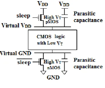
[image:1.595.329.514.511.665.2]MTCMOS is very effective technique to reduce the leakage current of circuits in the standby mode. The principle of the MTCMOS technique is the employment of low VT transistors to design the logic gates for which the switching speed is essential, and the high VT transistors also called sleep transistors are used to effectively isolate the logic gates in the standby state and reduce the leakage dissipation. The generic circuit structure of the MTCMOS circuit is shown in Figure 1.
Fig 1. MTCMOS circuit
2.1
MTCMOS design styles
A block is defined as a circuit whose elements share the same sleep signal. Depending on the system-level design, a block can be a whole chip, a core, a clock/VDD domain, a data path, and it can be a global bus (MTCMOS repeater) as well. Applying MTCMOS design to a block can be done in several ways. Different MTCMOS styles present different design tradeoffs.
2.1.1.
Global MTCMOS
[image:2.595.334.514.67.206.2]Global MTCMOS design as shown in figure 2 controls the whole block containing multiple local blocks, such as an entire chip or a full data path via a large centralized single sleep transistor.
Fig 2. Global MTCMOS
Global MTCMOS style has the lowest optimal total sleep transistor area. However, determining the optimal size of the global sleep transistor is hard, and impractical for large blocks. This complicates the design and leads, in most cases, to an over-sized sleep transistor, which in turn reduces the efficiency of global MTCMOS in terms of area. Regarding signal integrity, this style is also impractical since it suffers from degraded noise margin and large ground bounce in power/ground networks. It does not require intra block sleep signal routing but it suffers from high virtual power/ground lines sizing and routing complexity.
2.1.2.
Fine-Grain MTCMOS
[image:2.595.116.234.246.410.2]Here each gate has its own sleep device in the figure 3 shows two examples of an MTCMOS AND gate one with footer switch, other with a header switch. Determining the optimal sleep transistor size for fine-grain MTCMOS is easy. However, the area penalty is large. It has the best signal integrity since the virtual power/ground are embedded within the gates. It does not require virtual power/ground traces, but the sleep signal has to be delivered to all gates. It offers many desirable advantages in terms of signal integrity and sleep transistor sizing complexity. However, it suffers from a large area penalty, and it can only be considered when the sleep transistor area penalty can be tolerated [10].
Fig 3. Fine Grain Cells.
2.1.3.
Distributed MTCMOS
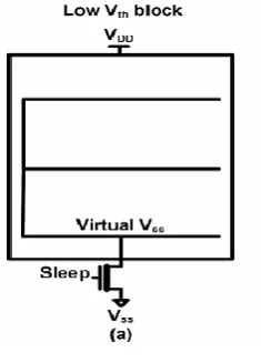
Distributed MTCMOS design as shown in figure 4 employs multiple sleep transistors for a single block. It in turn, can be applied in two ways.
Fig 4. Distributed MTCMOS
One way is cluster-based where a block is divided into clusters and each cluster has its own virtual power/ground and sleep device. Clustering is done based on the switching behavior of the gates to minimize the total sleep transistor area. Another way for distributed MTCMOS design is network-based (also known as coarse-grain) where many distributed sleep transistors are inserted between the actual and virtual power/ground networks inside the block, and these sleep transistors share the charge/discharge currents[8,9]. Distributed sleep transistor network was shown to be better than distributed clusters in terms of sleep transistor area and performance.
[image:2.595.344.507.308.468.2]2.2.
Short
comings
of
distributed
MTCMOS
In distributed MTCMOS, the sleep distribution network presents an overhead since the sleep signal has to be routed to all the sleep devices within the block. The sleep network is a multi-sink network which adds considerable routing complexity. Regular sleep transistor placement reduces the sleep signal routing complexity. However, the sleep signal still consumes precious routing resources and increases the total intra-block wire length, which in turn increases design cost. Moreover, sleep signal buffers consume leakage power in active and standby modes, and complicate buffer floor-planning and sleep signal routing.
3.
SELF-SLEEP BUFFER FOR
DISTRIBUTED MTCMOS
During active mode, the sleep transistors are turned on to maintain the functionality of the circuit. Although MTCMOS is a very effective technique, it introduces some overheads and design challenges. The area penalty due to the sleep transistors is one of MTCMOS overheads. Correct sizing of sleep transistor is required since over-sizing leads to an extra unnecessary area penalty and under-sizing leads to performance degradation and reduced noise margin. Signal integrity is another issue that should be considered during standby-to-active transition. Also, MTCMOS latches and flip-flops must retain the data in sleep mode. The energy and performance overheads of going from active-to-standby and standby-to-active should be minimized. Also, MTCMOS requires extra routing due to the virtual power/ground lines, and sleep signal distribution.
3.1. Self-sleep buffer
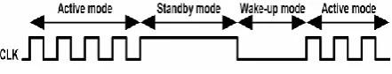
[image:3.595.328.529.286.429.2]In order to completely reduce power during standby mode, when a block goes into standby, its sleep transistors as well as its clock are turned off. If the block is a whole chip or if its clock is independent from the other blocks clock, clock gating can be done from the clock source. In the case of a multi-block system with global clock, clock-gating can be done locally from the node that distributes the clock signal to the idle block. This particular method uses the relation between sleep signal and the clock in order to eliminate the sleep distribution network. It is assumed that the clock is gated high, as shown in Figure 5. Before the block switches back to active mode, the clock goes low, which indicates a wake-up period.
Fig 5. Operation modes based on clock signal
The wake-up time depends on the distributed MTCMOS style being used. Also, several MTCMOS techniques that were previously proposed can be employed during this mode to achieve better signal integrity and lower energy. After the wake-up period, the block resumes its normal operation. Figure 6 presents a two stages dual-Vth self-sleep buffer. The
[image:3.595.58.279.628.670.2]self-sleep buffer outputs the sleep signal based on the clock. In the active mode and during the low-phase of the clock, node X is low and node S (sleep) is high. During the high-phase of the clock, node X starts charging. The self-sleep buffer should be designed such that at the worst corner, the voltage at node X cannot reach a level that causes a glitch at node S. Therefore, node S remains high during all the active period. Transistors N2 and P2 have high and low Vth, respectively. This increases the high-to-low switching threshold of the second stage inverter in the buffer, which helps in maintaining a glitch-free node S. Transistors N1 and P1 have minimum size channel length and width, in order to maintain the minimum possible clock loading. In the case of a large sleep device, extra stages can be added to the buffer to maintain the minimum possible clock load at the input. P1 and the weak PMOS stack have high Vth, and the channel length of the transistors in the weak PMOS stack equals to the maximum channel length (Lmax) allowed by the design/manufacturing rules[7].
Fig 6. Circuit of Self sleep buffer
The number of transistors in the weak PMOS stack is based on the desired peak voltage at node X during active mode VX (tduty), where tduty is the duty cycle of the clock since node X is charged during the entire high-phase of the clock. The active-mode peak voltage at node X equals
VX (tduty) = VDD(1=e - tduty/ RpCx
) (1)
where VDD is the supply voltage, CX is the total capacitance at node X, and RP is the sum of the weak PMOS stack resistance and transistor P1 on-resistance. δ is defined as the peak percentage swing at node X during the active mode, therefore
δ= VX (tduty) (2)
VDD
δ should be larger than zero, therefore
IP(on)>IN1(off) (3)
where is the current flowing through the weak PMOS stack and P1 during the high-phase of the clock, and
δ<βs(P2,N2) (4)
where is the ratio of high-to-low switching threshold of the second stage inverter (P2,N2) to VDD. Based on equation 1, tduty, VDD are known, and CX is determined based on the size of the second stage inverter, which in turn is determined based on the sleep device size. The number of weak transistors in the weak PMOS stack can be adjusted to achieve the desired δ, since
Rp = - tduty (5)
Cxloge(1-δ)
δ presents a tradeoff between mode power and active-to-standby delay and energy. Using a small δ achieves low active-mode power since the swing at node X is reduced, but it increases the active-to-standby delay of the buffer, as well as the active-to-standby short circuit current due to the slow slew rate at node X.
However, the active-to-standby delay is not important as the standby-to-active delay which affects the overall performance. The self-sleep buffer offers fast sleep-to-active transition through transistor N1 and P2. Transistor P3 acts as a booster which reduces the transition time at node X during active-to-standby transition, in order to reduce the short circuit power at the second stage inverter. However, P3 should have minimum size since it has to be weaker than N1.
Self sleep circuit with one, two and three transistors in the pmos stack (pull up) and nmos stack (pull down) is verified and observed that compared to noms stack in pull down, pmos stack in the pull up has better characteristics in terms of power and delay. As compared to one and two transistors in the stack, three transistors in the stack gives better values of delay and power.
3.2. Necessity of self-sleep buffer
MTCMOS power switch cells are widely used for on-chip power gating. In general, there are two approaches of MTCMOS power gating control. They are fine grain power gating and coarse grain or distributed power gating. In fine grain power gating, the sleep transistors are placed inside each standard cell, and thus have considerable area penalty. In contrast, coarse grain power gating shares sleep transistors to all of logic gates in the gated block and has very few area overhead. However, implementing coarse grain MTCMOS presents certain challenges to the design flow. These include power gating controller, sleep control propagation, buffer insertion and routing, power switch planning, power switch optimization, and power routing verification.
In distributed MTCMOS (cluster-based or network based), the sleep distribution network presents an overhead since the sleep signal has to be routed to all the sleep devices within the block. The sleep network is a multi-sink network which adds considerable routing complexity. Regular sleep transistor placement reduces the sleep signal routing complexity. However, the sleep signal still consumes precious routing resources and increases the total intra-block wire length, which in turn increases design cost.
Important metrics that greatly affect MTCMOS efficiency include active-to-sleep and sleep-to-active energy overheads. These metrics determine the minimum standby period that achieves overall power saving. Charging/discharging the sleep distribution network and its associated buffers introduce energy overhead comparable to the energy overhead of charging/discharging the virtual power/ground networks and turning-on the sleep transistors during standby-to-active mode, and is the major contributor in the active-to-standby energy overhead. Also, sleep signal network delay affects performance since it is also a major contributor in the total standby-to-active delay. Moreover, sleep signal network requires careful timing analysis to accurately determine the wake-up delay. With all these complexities related to sleep signal distribution in distributed MTCMOS design styles, and as the integration density of a single block continues to increase, design methods that take sleep signal distribution into account should be considered.
3.3. Sizing the sleep transistor
To estimate the size of the sleep transistor, the delay of a single gate at the absence of a sleep transistor can be expressed as[11]
τ
dα C
LV
dd (6)(V
dd-V
tL)
αwhere CL is the load capacitance at the gate’s output, VtLis the threshold voltage, is the velocity saturation index. In the presence of a sleep transistor, the delay of a single gate can be expressed
τd sleep
α
CL Vdd (7)
(Vdd-Vx-VtL)α
where Vx is the potential of the virtual ground. Assuming the circuit could tolerate a 5% degradation in performance due to the presence of the sleep transistor, therefore
τd = 95% (8) τsleep
Substituting for τd, τdsleep
and assuming α=1 for simplicity, Vx = 95% (9)
(Vdd-VtL)
Therefore Vx can be formulated as
Vx= 0.05(Vdd-VtL) (10)
The current flowing through the “linearly-operating” sleep transistor is expressed as
Isleep =μnCox(W/L)sleep[(Vdd-VtH)Vx- Vx 2
/2]
= 0.05μnCox(W/L)sleepX (Vdd-VtL) (Vdd-VtH) (11)
The size of the sleep transistor can be therefore expressed as
(W/L)sleep = Isleep (12) 0.05μnCox(Vdd-VtL) (Vdd-VtH)
of the sleep device is increasing, the power and delay are reduced to more than 35% and 44% respectively.
Table1. Power and delay values with different sizes of sleep device
Power/delay Active power
Standby power
delay
520 nm 29.49 uw 77 nw 69 ps
960 nm 30.53 uw 77 nw 43 ps
2 um 19.75 uw 77 nw 40 ps
4 um 19.57 uw 77 nw 39 ps
3.4.Advantages of self-sleep buffer
For distributed cluster-based and network-based MTCMOS, a self-sleep buffer is assigned to each sleep transistor. The number of stages and the transistor sizes of the self-sleep buffer are based on the size of the sleep device. The self-sleep buffer eliminates the need for distributing a sleep signal to all the sleep devices since it uses the available clock signal as its input. As a result, the total intra-block wire length, routing complexity, and interconnect buffers are reduced.
Sleep signal integrity during active mode is improved by the self-sleep buffers. The first reason for that is the very high resistance of the weak PMOS stack and P1, and the skewed second stage inverter. This makes the self-sleep buffer a noise filter during active mode, which helps in maintaining a glitch free sleep signal. The second reason is that the self-sleep buffer is driven by the clock signal which is the most well designed signal on the chip. Moreover, the delay and power
characteristics of the clock network are known, which eliminates the need for extra design effort in characterizing the delay and energy of the sleep network and maintaining its signal integrity. The active-to-sleep and sleep-to-active MTCMOS energy overheads are reduced with the self-sleep buffer due to the elimination of the charging/discharging of the sleep signal interconnect and its associated buffers. The reduction in MTCMOS energy overhead during mode transitions reduces the minimum standby period that is required to achieve overall power reduction, and helps in switching more frequently between active and standby modes.
4.
GENERAL PURPOSE
MICROPROCESSOR
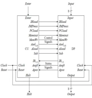
The custom datapath for the general purpose microprocessor is shown in Figure 7. The portion of the datapath for performing the instruction cycle operations is instruction register (IR), the program counter (PC), and the increment unit for incrementing the PC. In this design memory has 32 locations, hence the address, and therefore, the size of the PC and the increment unit must all be 5-bits wide.
The datapath contains a 2-to-1 multiplexer that is connected between the output of the PC and the memory address input. One input of this multiplexer comes from the PC, and the other input comes from the five least significant bits of the IR, IR4-0. The first is still for the fetch operation where the memory address is given by the content of the PC. The second type is for the four instructions, LOAD, STORE, ADD, and SUB, where they use the memory as an operand. Hence, the memory address for these four instructions is given by the five least significant bits of the IR. The select signal for this multiplexer is Meminst[12].
Fig 8. Control unit of the General purpose computer
Fig 9. Bolck diagram of the General Purpose Microprocessor.
4.1
Results
In this paper the self sleep circuit with better performance characteristics is designed and used in the simulation of different blocks of general purpose microprocessor like instruction register, program counter, accumulator, RAM and control unit. All the blocks of the design are designed using cadence tools, GPDK library 90 nm Technology. The fine grain values are compared with distributed MTCMOS and observed the reduction in number of nets, transistors and leakage power as shown in table2. Table3 and table 4 show small savings in average power and great savings in leakage power when self sleep is introduced at the distributed level.
Table 2. Comparison of Fine grain and Distributed
Method Fine grain Distributed MTCMOS
Transistors 1273 1260
Nets 1059 931
Leakage Power 3.14uW 2.49uW
Table 3. Average power comparison of different blocks
DESIGN MODULE Power
without sleep
Power with self- sleep
ACCUMULATOR 23.48uW 22.26uW
PROGRAM
COUNTER 15.5uW 14.32uW
INSTRUCTION
REGISTER 23.6uW 22.33uW
32*8 SRAM 3.041mW 2.419mW
DATA PATH 18.11mW 13.95mW
[image:6.595.310.549.88.279.2]CONTROL UNIT 62.41uW 63.29uW
Table 4. Leakage power comparison of different blocks
DESIGN MODULE
Power without Sleep
Power with Self-sleep
ACCUMULATOR 1.73uW 98.72nW
PROGRAM
COUNTER
1.39uW 77nW
INSTRUCTION
REGISTER 1.78uW 98.5nW
32*8 SRAM 567uW 166uW
DATA PATH 865uW 393uW
CONTROL UNIT 8.13uW 2.31uW
5.
CONCLUSION
In this work self sleep circuit is verified for better performance characteristics by placing different number of transistors in PMOS stack and NMOS stack for different loads. The number of transistors in the stack is also varied and it is observed that with a minimum of three transistors the performance characteristics are good.
[image:6.595.95.257.296.468.2]6.
ACKNOWLEDGMENTS
Our sincere thanks to the management of CVR College of Engineering for having provided Cadence tools to develop this design.
7.
REFERENCES
[1] S. Mutoh et al., “1-V power supply high-speed digital circuit technology with multithreshold-voltage CMOS,” Jour. Solid- State Circuits, vol. 30, pp. 847-854, Aug. 1995.
[2] J. Kao, A. Chandrakasan, D. Antoniadis, “Transistor sizing issues and tool for multi-threshold CMOS technology,” in Proc. IEEE/ACM Design Automation Conf., pp. 409-414, June 1997.
[3] J. Kao, S. Narendra, A. Chandrakasan, “MTCMOS hierarchical sizing based on mutual exclusive discharge pattern,” in Proc. IEEE/ACM Design Automation Conf., pp. 495-500, June 1998.
[4] S. Kim, S. V. Kosonocky, D. R. Knebel, and S. Stawiasz, “Experimental measurement of a novel power gating structure with intermediate power saving mode,” in Proc. IEEE Int. Symp. On Low Power Elec. Design, pp. 20-25, August 2004.
[5] S. Kim, S. V. Kosonocky, D. R. Knebel, “Understanding and minimizing ground bounce during mode transition of power gating structures,” in Proc. IEEE Int. Symp. On Low Power Elec.Design, pp. 22-25, August 2003.
[6] A. Ramalingam, A. Devgan, and D. Z. Pan, “Wakeup scheduling in MTCMOS circuits using successive relaxation to minimize ground bounce,” Jour. Of Low Power Electronics, vol.3, no. 1, 2007.
[7] Charbel J. Akl and Magdy A. Bayoumi “Sleep buffer for distributed MTCMOS design” in Proc. IEEE/ACM Int. Conference on VLSI design, pp. 673-678, 2008
[8] C. Long, and L. He, “Distributed sleep transistor network for power reduction,” IEEE Trans. VLSI Syst., vol. 12, no. 9, Sep. 2004.
[9] Shi, D. Howard, “Sleep transistor design and implementation – simple concepts yet challenges to be optimum,” in Proc. Int. Symp. VLSI Design, Automation and Test, pp. 1-4, April 2006.
[10] V. Khandelwal and A. Srivastava, “Leakage control through fine-grain placement and sizing of sleep transistors,” in Proc. IEEE/ACM Int. Conference on CAD, pp. 533-536, 2004.
[11] Mohab Anis,Shawki Areibi and Mohamed Elmasry, “Design and Optimization of Multithreshold CMOS(MTCMOS) Circuits”, IEEE Trans on CAD of ICs and systems, pp. 1324-1342, 2003.