http://dx.doi.org/10.4236/cs.2016.73013
VELAN: Variable Energy Aware Sense
Amplifier Link for Asynchronous
Network on Chip
Erulappan Sakthivel
1, Veluchamy Malathi
2, Muruganantham Arunraja
1 1Electrical and Electronics Engineering, The Siliconharvest, Madurai, India2Electrical and Electronics Engineering, Anna University Regional campus, Madurai, India
Received 13 February 2016; accepted 26 March 2016; published 31 March 2016
Copyright © 2016 by authors and Scientific Research Publishing Inc.
This work is licensed under the Creative Commons Attribution International License (CC BY). http://creativecommons.org/licenses/by/4.0/
Abstract
A real time multiprocessor chip paradigm is also called a Network-on-Chip (NoC) which offers a promising architecture for future systems-on-chips. Even though a lot of Double Tail Sense Am-plifiers (DTSA) are used in architectural approach, the conventional DTSA with transceiver exhi-bits a difficulty of consuming more energy and latency than its intended design during heavy traf-fic condition. Variable Energy aware sense amplifier Link for Asynchronous NoC (VELAN) is de-signed in this research to eliminate the difficulty, which is the combination of Variable DTSA cir-cuitry (V-DTSA) and Transceiver. The V-DTSA circir-cuitry has following components such as bootable DTSA (B-DTSA) and bootable clock gating DTSA (BCG-DTSA), Graph theory based Traffic Estimator (GTE) and controller. Depending upon the traffic rate, the controller activates necessary DTSA modules and transfers information to the receiver. The proposed VELAN design is evaluated on TSMC 90 nm technology, showing 6.157 Gb/s data rate, 0.27 w total link power and 354 ps latency for single stage operation.
Keywords
Network-on-Chip (NoC), Double Tail Sense Amplifier (DTSA), Clock Gating (CG)
1. Introduction
NoC is a booming area for designing various applications like multimedia, telecommunication, and real time task [1]. Previous researches mainly focus on low power, high speed and scalability in NoC [2]. Algorithmic [3]
introducing external or internal sense amplifier (SA) in on-chip communication [5]. In addition to the transmitter section (TXS), the pre emphasis capacitance (PEC) is added for high speed and energy reduction in on-chip communication, it requires DC bias circuits at the receiver section (RXS). To overcome this issue, voltage sense amplifier is introduced and tested in 90 nm CMOS cross coupled circuit [6]. In small circuit application, user can’t identify the worth of voltage SA, so it is refined into Double Tail Sense Amplifiers (DTSA). This DTSA with transceiver consists of PEC at the transmitter and DTSA at RXS [7]. In a recent paper [8], we presented transceiver with Reconfigurable DTSA (R-DTSA) to achieve the performance improvement. Both [7] and [8]
has achieved a reduction in data rate and link power. In this paper, we have concentrated on improving the la-tency parameter by adapting the bootable concept in DTSA. Bootable concept is the combinations of clock ena-ble [9] and clock gating [10]. A low power consumption model is developed and implemented in many real time applications. CG low power design approach at RTL TSMC 45 nm CMOS application is tested in [11]. CMOS VLSI design has taken us to real working chips that rely on controlled charge recovery to operate at significantly lower power dissipation levels than their existing counterparts. The energy recovering circuits [10] are applied in microcontrollers, memory devices, display drivers, grouped clock networks and other real time applications. CG-SAFF (sense-amplifier flip-flop) [12] circuit exhibits high speed and low energy. The switching activity and delay of various flip-flops are compared with CG-SAFF. In [13], the performance improvement achieved in networks with respect to network traffic modeling based on synthetic traffic. The traffic estimator and generator are introduced for QoS in [14], to generate and estimate the real time traffic data in on-chip communication. In this proposed VELAN design, we followed the Traffic generator [8] and Graph Theory based Traffic Estimator (GTE) [8]. To achieve higher performance under various traffic conditions in on-chip networks, energy recovery clocking [15] concept is introduced in DTSA called M-DTSA [8] and clock gating [13] concept in M-DTSA [8]
called MCG-DTSA [8]. Similar to Schinkel et al. and Sakthivel et al., this VELAN design is validated. In the proposed analysis the Individual and proposed sensor amplifier functionalities are validated. The Proposed V-DTSA module is encapsulated into the receiver section of router construction in NoC. The Proposed Perfor-mance metrics like delay, datarate, energy and static power consumption are observed and compared with con-ventional works.
The key contributions of this work are as follows.
• Schinkel et al. has proposed the DTSA with low power and high speed architecture.
• The conventional DTSA is not evaluated under high traffic scenario and here we examined same DTSA un-der various traffic scenarios. We have found that the traffic affects the performance of conventional DTSA. To solve this issue R-DTSA is proposed.
• This R-DTSA is a combination of four DTSA, which is validated with various traffic scenarios and the re-sults are reported in Sakthivel et al., which is better than Schinkel et al.
• Even though R-DTSA is more advantageous than DTSA, but some issues are remaining such as the more latency, high area and high cost. To overcome these issues and reduce the complexity of R-DTSA, we fo-cused and developed a new DTSA which was called V-DTSA.
• This V-DTSA provides a better performance than DTSA and R-DTSA in terms of all the parameters men-tioned in the conventional work.
• We have introduced the V-DTSA based NoC which was used to provide a better performance than conven-tional DTSA and R-DTSA under various Traffic scenarios.
• To construct the V-DTSA, we used Bootable concept into both DTSA and CG-DTSA circuits.
• Similar to the previous work R-DTSA, we introduced the same Graph theory based Traffic Estimator (GTE). • The top modules of V-DTSA are namely B-DTSA, BCG-DTSA, GTE and controller.
• The primary part of this proposed work is an Analysis of Various Sense amplifiers and selection of suitable DTSA for performance comparison.
• This work is aimed to produce new latency aware NoC design based on V-DTSA under various traffic sce-narios.
• The performance parameters such as Delay, Data rate, Power, Energy, area and more parameters are ob-served and reported in Section 4.
2. System Model
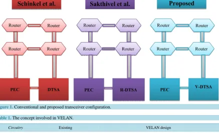
For better data communication in NoC architecture, conventional transceiver has PEC in TXS and DTSA circuit in RXS. Schinkel et al. and Sakthivel et al. transceiver for NoC’s and proposed VELAN design is shown in Figure 1. The use of capacitance in TXS is to reduce power dissipation. In NoC circuitry communication dis-turbance occurs because of noise and crosstalk [16]. The transceiver with a Differential Interconnect Twist (DIT) provides a high performance improvement. On Early stage, bidirectional interconnects are used. The EM field solver is used to analyze interconnects. The CMOS with 1.2 V, 6 M technology is used for interconnects as in [7] [8]. Table 1 shows the concept involved in VELAN and which is compared with existing design.
3. Proposed System
The conventional transceiver configuration is compared with the proposed Transceiver configuration which is shown in Figure 1. The proposed VELAN design consists of V-DTSA circuitry for reducing the power con-sumption of data transmission and latency. The proposed work consists of four stages, namely selection, analy-sis, and design and performance comparison.
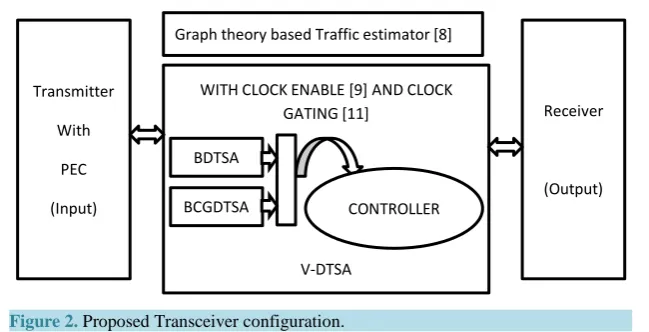
In the first stage of the work, suitable SA is selected with respect to the power comparison in both sleep and active mode [8] (observed M-DTSA, MCG-DTSA for further process). After clock enable [9], both DTSA’s re-fined into B-DTSA and BCG-DTSA. In the second stage, selected SA’s (DTSA, B-DTSA and BCG-DTSA) are applied with high traffic (HT) and low traffic (LT) and then the energy comparison is analyzed. In the third stage, we designed the V-DTSA circuitry for complete transceiver. Finally, we compared our results with [7][8]. The block diagram of VELAN design is shown in Figure 2. This proposed system consists of PEC with TXS, GTE [8], V-DTSA circuitry and RXS. The Graph theory Traffic Estimator (GTE) [8] is used to estimate the traffic rate of transmitting data. Based on the data, traffic controller is used to select the corresponding DTSA available in V-DTSA circuitry.
Clock gating has been proved best, when there are more number of flip-flops (coarse grained) in the circuit,
[image:3.595.95.533.408.674.2]Figure 1.Conventional and proposed transceiver configuration.
Table 1.The concept involved in VELAN.
Circuitry Existing VELAN design
[7][9] DTSA, M-DTSA with bootable option
[10][11] CG, ERC MCG-DTSA with bootable option
Figure 2.Proposed Transceiver configuration.
since it is independent of the circuit size. In a fine grained system (fewer lip-flops) clock enable achieves better energy conservation, since, the power consumption of this option is very linear with the number if flip-flops. As clock enables activates only a part of the circuit this works better on a partially active task. As clock gating acti-vates the complete circuit, works well with the task needing the whole circuit. And it’s proved and experimen-tally validated in FPGA platform by Oliver et al. Based on these modules, we have constructed our proposed circuit
4. Proposed Work and Its Module Details
The section discusses about energy recovery clocking Circuit, Clock Gating circuit, bootable concept, low swing transmitter, optimal swing receiver, a V-DTSA components, graph theory based traffic estimator and controller and complete transceiver for proposed DTSA.
4.1. Energy Recovery Clocking (ERC) Circuit
Mahmoodi et al. have introduced an energy recovery clock technique in flip-flops that operates with single- phase sinusoidal clocks. In ERC circuit, AC supply voltage is used to recycle the stored energies on their capa-citance while standard supply voltage is used for the rest of the circuits. The schematic representation of the ERC is observed from [12] for energy recovery clock generation. The energy recovery technique is implemented in DTSA circuit to accomplish the power reduction in NoC architecture.
4.2. Clock Gating (CG) Circuit
Tirumalashetty et al. have introduced clock gating technique in sequential circuits for low power design. In CG circuit, universal logic gate is used for masking the local clock signal to eliminate an energy recovery scheme from the remaining capacitances in fan-out circuit. The schematic representation of CG is observed from [11]
for clock gating generations. An energy loss occurs due to non-adiabatic switching between the device oscilla-tors and the resistance of the clock circuit and it can be eliminated by applying clock gating technique in DTSA circuit
4.3. Bootable Concept
In general, DTSA has precharge and evaluation phases of operation. The slow rising and falling transitions of the resonant clock will cause overlap between these two phases, which results in short-circuit current. The main purpose of the bootable clocking scheme is to reduce short-circuit power by switching the precharging transis-tors for a portion of clock period.
4.4. Low Swing Transmitter
In a low swing transmitter, large transmitters are required to drive the bus with adequate speed which results in reduction of transmitter efficiency. To overcome this issue and achieve high data rate, Schinkel et al. and
Sak-Transmitter
With
PEC
(Input)
Graph theory based Traffic estimator [8]
WITH CLOCK ENABLE [9] AND CLOCK GATING [11]
V-DTSA
Receiver
(Output) BDTSA
thivel et al. are used a capacitive pre-emphasis transmitter that uses a series capacitance to drive the bus with low swing. The series capacitance in transmitter is used to drive the bus and reduces the swing factor. The tech-nical concepts of proposed low swing transmitter with PEC are similar to that of Schinkel et al. and Sakthivel et al. The technical parameters of the Full Swing (FS), Multi VDD Mode (MVM) Capacitive Low Swing trans-mitter (CLS) are tabulated in the Table 2.
4.5. Optimal Swing Receiver
The most commonly used data receivers in a low swing transceiver are clocked comparators and sense amplifier. The comparators are used to regenerate the voltage to full swing. But the sense amplifier is a very fast circuit that regenerates the voltage, samples the incoming data and realign at the reception's end with respect to the clock signal. The sense amplifier circuit is split into two tails to avoid transistor stack, which is called DTSA is used in the receiver section of proposed transceiver.
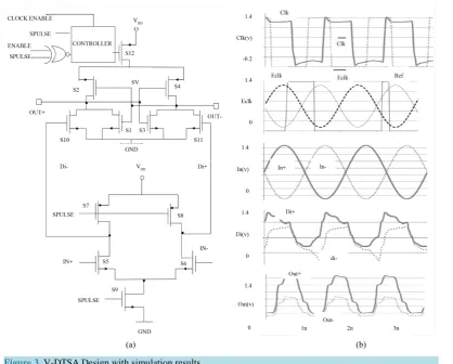
4.6. V-DTSA
The latency and the power dissipation of the DTSA is the basic building block of the clock distribution network that plays a vital role in NoC, an ensured design is needed to achieve low power and small latency [17].
[image:5.595.88.541.466.719.2]To gain maximum power reduction of data transmission in NoC architecture, the proposed work presented a variable energy aware sense amplifier design with V-DTSA circuit. The purpose of the V-DTSA circuit is to vary the DTSA module according to the traffic rate of the data. It consists of Graph theory based Traffic Esti-mator [8], controller and DTSA modules, namely B-DTSA and BCG-DTSA. The ERC concept is implemented in DTSA circuit is called Modified-DTSA (M-DTSA). The clock gating technique is implemented in the M- DTSA [8] module by adding logical NOR which is a gate to the circuit called Clock Gating Modified-DTSA (MCG-DTSA) [8]. After applying clock enable [9] both circuits are called B-DTSA and BCG-DTSA. The func-tional diagram of the V-DTSA module and its simulation result is shown in Figure 3, which consists of transis-tors S1-S12 with S-pulse signal, logical NOR gating and controller. The GTE estimates the traffic rate of the data with respect to the specification which is given in Table 3. After estimating the traffic rate of the data, the control signal is sent to the controller to activate the DTSA module according to the traffic rate (LT/HT). If the input data is estimated as low traffic (LT), then the controller activated the S-pulse (ERC output) as input to the DTSA circuit. The controller enables the output of the logical NOR gate to the DTSA circuit for HT. Therefore,
Table 2.The technical concept involved in Velan.
MODES TECHNOLOGY &
SPECIFICATION SUPPLY VOLTAGE VOLTAGE DRIVER SIZE
FS
1.2 V, 6 metal ,90 nm CMOS 2 mm, Rwire = 400 Ω
1.2V 1.2 V Wn = 8 µm
Wp = 20 µm
MVM VDDH = 1.2V
VDDL = 1.08V 120 mv
Wn = 8 µm Wp = 20 µm
CLS 1.2 V 120 mv Wn = 1.6 µm
[image:5.595.85.538.591.717.2]Wp = 4 µm
Table 3.The overall transceiver performance comparison.
MODE TRAFFIC
MODE DATA RATE GB/S (DATA RATE IMPROVEMENT %) TECHNOLOGY LINK POWER (W) LATENCY SINGLE/FIVE STAGE OPERATION
DTSA [7] Low (LT) 5.0 (80%) 90 nm 0.8 300/1500
DTSA High (HT) 4.2 (67.2%) 90 nm 1.4 454/2270
DTSA Average 4.6 (73.6%) 90 nm 1.1 377/2950
R-DTSA [8] Average 6.1 (97.6%) 90 nm 0.32 590/2950
Figure 3.V-DTSA Design with simulation results.
the transistor dimensions of the proposed double-tail sense amplifier are optimized comparative to each other to get the lowest offset standard deviation per unit of power cost. Width scaling (or impedance or area scaling) can consequently be useful to all the transistors composed to match the offset standard deviation to the preferred re-quirement [7] while preserving the original speed characteristics
4.7. Graph Theory Based Traffic Estimator and Controller
The optimal weight equation is used for the TE design follows from [15]. The GTE [8] estimates the traffic rate and compares with the given threshold value and then it selects the corresponding DTSA module in V-DTSA circuitry via the controller. In order to reduce complexity in [8], two DTSA modules eliminated and traffic modes are merged into four states to two states, namely HIGH (HT) and LOW (LT).
4.8. Complete Transceiver
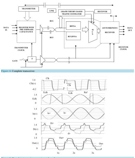
The complete transceiver circuit is made of transmitter with pre-emphasis capacitance connected to the receiver with the V-DTSA module via DIT [7][8]. The V-DTSA circuitry consists of B-DTSA and BCG-DTSA that gets the input data through the bus. The traffic estimator estimates the traffic under low or high condition using graph theory method and enables suitable DTSA by sending selected signal to the MUX. All other techniques are adapted same from [8] and the complete transceiver is shown in Figure 4 and simulation results are shown in Figure 5.
5. Results and Discussion
5.1. Performance Measure-Analytical Model
Figure 4.Complete transceiver.
Figure 5.Complete transceiver experimental result.
mance measurement in NoC. The performance measures of delay, data rate, energy, static power consumption, average latency, throughput, energy per useful flits switching factor and analysis in a network-on-chip. The de-finitions of these metrics are summarized here.
1) To measure the latency of flows, it is essential to evaluate the packet waiting periods for routers.
2) The power consumption and Link power are considered recursively for every communication path starting from the terminus section.
4) Data rate is measured, based on all communication paths beginning of the terminus section. 5) Average latency is a time interval between the stimulation and response.
6) Throughput is the rate of production or the rate at which something can be processed. 7) Energy per useful flits is obtained with respect to the number of flits.
8) Switching factor is the probability of output switching.
5.1.1. Latency
In each node Ni, the latency LnocNi is defined using network calculus from Bhat et al.[18] and Sakthivel et al.
[19] as follows.
LnocNi wij lat ii
S T w
= + (1)
where
Switis the service bandwidth and Tlat is the latency.
5.1.2. Power
1) Link Power
In Bhat et al.[18] and Sakthivel et al.[19], the power models practical is used for a NoC Router. The power model is considering the cross-coupling effect for N-wire interconnects. The total power is calculated for an N-wire link per unit length as follows:
(
)
(
)
2
, ,
1 2
link wire sv self saw Cou Cou saw short bias wire leak gate
P = N V C α +C α f +Nτα VI ⋅f + ⋅N VI +VI (2)
where
Nwire is the total number of wires in the link
Cselfand Ccoupl are the self and coupling capacitance of a wire and neighboring nodes respectively, αsaw is the switching activity on a wire,
αCou is the switching activity with respect to the adjacent wires, τ is the short circuit period,
Vsv is the supply voltage,
Ishort, bias, wire and Ileak, gate are currents.
2) Static Power consumption
The static power dissipation can be defined from Bhat et al.[20] and Sakthivel et al.[21] as follows in Equa-tion (3).
, ,
static bias wire leak gate
P =VI +VI (3)
5.1.3. Energy
An energy spent at upper levels owing to that one bit of data is sprinkled from one router (R1) to another router (R2) via the links is a efficacy of the number of routers and the number of links. The total energy
ε
nergy t( )
can be intended as follows (Bhat et al.[18]; Sakthivel et al.[19])
( )
1 consumed@time( )
1consumed@switch,link( )
s
l N
N
i j
nergy t t t
ε =
∑
=ε +∑
=ε (4)where
ε
consumed@time( )
t is the energy spent, at time t, on the link li,ε
consumed@consumed@time( )
t is the energy con-sumed inside the switch sw and NlinkandNswitch are the number of links and switches respectively involved in transporting the application flows. The total energy consumption can be calculated using Network Calculus arrival curves as follows Bhat et al.[18] and Sakthivel et al.[19].5.1.4. Data Rate
A FIFO buffer with an identified capacity from Sakthivel et al.[19], substitutes a data burst with presumed size, and the arrival data rate is distinct as follows.
[ ]
size inteerval_time 1where, Psize is the packet size and Pinterval_time and N total input flits. The smallest data unit is a bit in the analyti-cal model and it is a frame with bounded size in the simulation model.
5.1.5. Average Flit Latency
Average Flit Latency is defined as the ratio between Flit Delay and Number of flits received. It is given Equa-tion (6) (Yu & Ampadu [20])
1Flit Delay
Average Flit Latency
M
i i
M
=
=
∑
(6)(
flit_sent_t flit_received_i)
1 M
i T T
M
= −
=
∑
(7)where, M = Number of flits received
5.1.6. Average Throughput
Average Throughput is defined as the ratio between P and Number of IP cores. It is given in Equation (8) (Yu & Ampadu [20])
Average Throughput P
N
= (8)
P is defined as the ratio between Total Received Flit and Total Simulation Time. It is given in Equation (9)
1
Total Flit Received Total Simulation Time
N
i
i
P= =
∑
(9)where N = Number of IP cores
5.1.7. Switching Factor
The ratio between the Switched in port and total simulation cycle count is called as switching factor. It is given in Equation (10) (Yu & Ampadu [20])
(
5)
1 1 1Switched in port
Switching Factor
C N
k
i j k j
C
= = =
=
∑ ∑ ∑
(10)where N = Number of IP cores/Routersand, C = Total Simulation Cycle Count
5.1.8. Energy per Useful Flit
Energy per Useful Flit is defined as the ratio between energy and Total Error Free Flits Received. It is given in Equation (11) (Yu & Ampadu [20])
1 1Energy
Energy per Useful Flit
Total Error Free Flits Received
C N
j i= j=
=
∑ ∑
(11)5.2. Experimental Section Analysis
realis-tically reveal all types of traffic that will traverse the network, but GT-based traffic pattern [8] provides a rea-sonable measurement for the performance of this method.
The NoC VHDL-synthesized code is made to evaluate 90-nm TSMC CMOS technology under a 500-MHZ operating frequency, a supply voltage of 1.8 V and a switching factor 0.5. In V-DTSA module, the controller part is made as a model and that is synthesized in 90 nm TSMS CMOS technology. To evaluate the performance of the proposed V-DTSA circuitry, comparisons has been performed with other recent works includes DTSA [8]
and reconfigurable DTSA [9]. The Sleep mode and Active mode power consumption are tested with CG and without CG and then the results are presented in [8]. The power is compared to DTSA modules such as Single- ended Conditional Capturing Energy Recovery (SCCER) [12], DCCER [12], Static Differential Energy Recov-ery (SDER) [12], Pulsed Flip Flop (PFF) [22], M-DTSA [8], MCG-DTSA [8]. The clock enable concept (boota-ble) is applied to conventional DTSA circuitries (M-DTSA [8], MCG-DTSA [8].
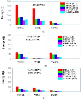
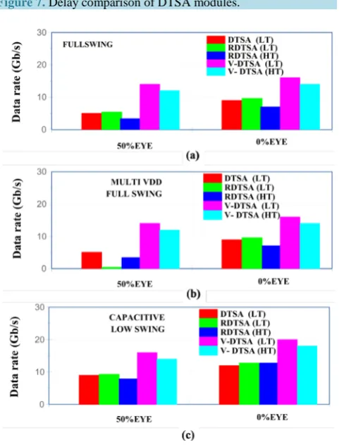
A mathematical expression for technical evaluation is similar to [20]. The energy consumption, delay, data Rate and static power consumption results are presented in Figures 6-9. The DTSA, R-DTSA and V-DTSA circuitry results are estimated under HT and LT. The overall comparison of various parameters (energy con-sumption, static power, and delay and data rate) with existing work is shown in Table 3.
The overall results of VELAN design give superior results than conventional design. The conventional me-thod has achieved latency of 300/1500 ps, under single/five stage operation. The latency result of the proposed work is better under average traffic condition than [7][8] (354/1770 ps).
[image:10.595.171.457.350.705.2]The following experimental parameters can be used to measure the NoC parameters, namely Average Flit La-tency (AFL), Average Throughput (AT), Switching Factor (SF), and energy per useful flit. The above parame-ters are obtained using mathematical equations [20]. The Flit rate defines the rate at which packets are injected
Figure 7.Delay comparison of DTSA modules.
[image:11.595.194.435.389.705.2]Figure 9.Static Power comparison of DTSA modules.
into the system which is noted in flit/node/cycle.
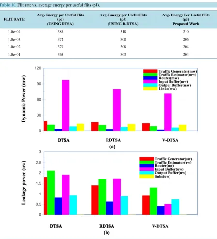
The dynamic power and the leakage power are tested in different terminals such as the traffic generator, GT- based traffic estimator [8], the router, the input buffer, the output buffer, and links under various approaches ([7] [8] and proposed work). The results are presented in Table 4 and Table 5, and the comparison plots are plotted in Figure 10. It is inferred that the proposed work gives a superior result in terms of power consumption, com-pared with the [7][8] works.
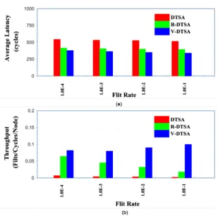
The performance comparison of the traffic injection rate, the throughput and the average flits latency are tested. The results are presented in Table 6 and Table 7 and the comparison plots are plotted in Figure 11. The performance comparison of the flit rate, throughput and the average flits latency are tested. The results are pre-sented in Table 8 and Table 9 and the comparison plots are plotted in Figure 12. It is inferred that the proposed work gives a superior result in terms of throughput and latency, compared with the [7][8] works. The perfor-mance comparison of energy per useful flits with flit rate is tested. The results are presented in Table 10 and the comparison plots are plotted in Figure 13. It is inferred that the proposed work gives a superior result in terms of energy consumption, compared with the [7][8] works.
Schinkel et al. have estimated bandwidth per cross-sectional area (BW/CSA). The differential wires are used in the proposed design which operates at high speed and low swing. The Technical specification used for the proposed work is mentioned in Table 2. The 1.2-V, 6-M, 90-nm CMOS process, metal-4 wires with 0.54 m width and a 0.32 m spacing is used. The conventional system has the highest BW/CSA in total NoC core. In or-der to estimate total wire-length, the following constraints are made in Schinkel et al. Rwire = 200 ohm/mm2; Cwire = 280/mm2; single differential channel (SDC) = 1.72 µm. Let the link has a length of L = 2 mm and a width W = 64 bits Area occupied of both directions = 2 × W × L × SDC = 2 × 2 × 64 × 1.75 µm = 0. 44 mm2 when placed in one metal layer. For five metal layers with mesh topology configuration, the total link area in Schinkel
Table 4.Dynamic power of various approaches with transceiver. WORK TRAFFIC GENARATOR (mw) TRAFFIC ESTIMATOR (mw) ROUTER (mw) INPUT BUFFER (mw) OUTPUT BUFFER (mw) LINKS (mw)
(USING DTSA) 18 11.4 3.4 97 8 13.2
(USING
R-DTSA) 16 10.6 2.8 80 7.2 12.6
PROPOSED
WORK 14 8.3 2.1 71 6.1 11.3
Table 5.Leakage power of various approaches with transceiver.
WORK TRAFFIC GENARATOR (µw) TRAFFIC ESTIMATOR (µw) ROUTER (µw) INPUT BUFFER (µw) OUTPUT BUFFER (µw) LINKS (µw)
(USING DTSA) 1.8 2.1 0.81 1.91 0.91 0.00096
(USING
R-DTSA) 1.4 1.7 0.62 1.73 0.88 0.00077
PROPOSED
WORK 0.9 1.3 0.41 0.51 0.73 0.00065
Table 6.Traffic injection rate vs. throughput.
TRAFFIC INJECTION RATE (Packet/Cycle/Node) THROUGHPUT (Cycles)
0.1 0.26
0.2 0.38
0.3 0.444
0.4 0.53
0.5 0.61
Table 7.Traffic injection rate vs. average flits latency.
TRAFFIC INJECTION RATE (Packet/Cycle/Node) AVERAGE FLITS LATENCY (Flits/Cycle/Node)
0.1 218
0.2 311
0.3 387
0.4 437
0.5 498
Table 8.Average latency vs. flit rate.
FLIT RATE
AVERAGE LATENCY (Cycles) ( USING DTSA)
AVERAGE LATENCY (Cycles) (USING R-DTSA) AVERAGE LATENCY (Cycles) PROPOSED WORK
1.0e−04 544 416 380
1.0e−03 532 407 363
1.0e−02 527 401 351
Table 9.Throughput vs. flit rate.
FLIT RATE
THROUGHPUT (Flits/Cycle/Node)
(USING DTSA)
THROUGHPUT (Flits/Cycle/Node) (USING R-DTSA)
THROUGHPUT (Flits/Cycle/Node)
Proposed Work
1.0e−04 0.0068 0.0640 0.0821
1.0e−03 0.0041 0.0452 0.0800
1.0e−02 0.0036 0.0321 0.0903
1.0e−01 0.0023 0.0183 0.1000
Table 10.Flit rate vs. average energy per useful flits (pJ).
FLIT RATE
Avg. Energy per Useful Flits (pJ)
(USING DTSA)
Avg. Energy per Useful Flits (pJ)
(USING R-DTSA)
Avg. Energy Per Useful Flits (pJ)
Proposed Work
1.0e−04 386 318 210
1.0e−03 372 308 206
1.0e−02 370 308 204
[image:14.595.88.537.211.706.2]1.0e−01 365 303 204
Figure 11.Traffic injection rate vs. throughput, average flits latency.
[image:15.595.159.469.395.706.2]Figure 13.Flitrate vs. average energy per useful flits.
when compared with R-DTSA based NoC. Therefore, in this V-DTSA based NoC consume lesser area usage and low cost than R-DTSA.
The power consumption and latency are estimated through the synthesizable VHDL model in the Synopsis environment with 90 nm technology. The following performance metrics Energy, Static, Dynamic power are measured and compared with [7] and [8]. The experimental results of VELAN design shows better performance than those of [7] and [8].
6. Conclusion
The proposed work is summarized into four stages, namely selection, analysis, design and performance compar-ison. In the first stage, among various sense amplifiers circuits few sense amplifiers are selected to form V- DTSA and power comparison is made in both active and sleep modes (M-DTSA and MCG-DTSA selected and refined into B-DTSA, BCG-DTSA). In the second stage, energy comparison is analyzed by applying LT (18 Gb/s/113fJ) and HT (12.8 GB/s/164fJ) traffics on selected DTSA modules (DTSA, B-DTSA and BCG-DTSA). As the result of analysis, power reduction is achieved in B-DTSA for LT and BCG-DTSA for HT. On the third stage, we designed V-DTSA circuit with GTE, Controller and DTSA modules. The GTE estimates the traffic rate and controls the Controller to select B- DTSA for LT and BCG-DTSA for HT. At the final stage, the result of the overall transceiver circuit (VELAN) under average traffic mode is obtained as 6.157 Gb/s data rate, 0.27 w link power and latency of 440 ps/2200ps for single/five stage operation. When compared with conventional methods, the results in VELAN design show performance improvement of 98.512% (data rate) and 18.51% re-duction (link power).
References
[1] Marculescu, R. and Bogdan, P. (2007) The Chip Is the Network: Toward a Science of Network-on-Chip Design. Foundations and Trends® in Electronic Design Automation, 2, 371-461. http://dx.doi.org/10.1561/1000000011
[2] Moraes, F., Calazans, N., Mello, A., Möller, L. and Ost, L. (2004) HERMES: An Infrastructure for Low Area Over-head Packet-Switching Networks on Chip. Integration, the VLSI Journal, 38, 69-93.
http://dx.doi.org/10.1016/j.vlsi.2004.03.003
[4] Fang, J.W., Wong, M.D., Chang, Y.W. (2009) Flip-Chip Routing with Unified Area-I/O Pad Assignments for Package- Board Co-Design. Proceedings of the 46th Annual Design Automation Conference, San Francisco, 26-31 July 2009, 336-339. http://dx.doi.org/10.1145/1629911.1630002
[5] Liu, Y., Liu, G., Yang, Y. and Li, Z. (2011) A Novel Low-Swing Transceiver for Interconnection between NoC Rou-ters. 2011 7th International Conference on Digital Content, Multimedia Technology and Its Applications (IDCTA), Busan, 16-18 August 2011, 39-44.
[6] Larsson, P. (1998) Resonance and Damping in CMOS Circuits with On-Chip Decoupling Capacitance. IEEE Transac-tions on Circuits and Systems I: Fundamental Theory and ApplicaTransac-tions, 45, 849-858.
http://dx.doi.org/10.1109/81.704824
[7] Schinkel, D., Mensink, E., Klumperink, E.A., Van Tuijl, E. and Nauta, B. (2009) Low-Power, High-Speed Transceiv-ers for Network-on-Chip Communication. IEEE Transactions on Very Large Scale Integration (VLSI) Systems, 17, 12-21. http://dx.doi.org/10.1109/TVLSI.2008.2001949
[8] Sakthivel, E., Malathi, V. and Arunraja, M. (2014) MATHA: Multiple Sense Amplifiers with Transceiver for High Performance Improvement in NoC Architecture. Microprocessors and Microsystems, 38, 692-706.
http://dx.doi.org/10.1016/j.micpro.2014.06.001
[9] Oliver, J.P., Curto, J., Bouvier, D., Ramos, M. and Boemo, E. (2012) Clock Gating and Clock Enable for FPGA Power Reduction. 2012 VIII Southern Conference on Programmable Logic (SPL),Bento Goncalves, 20-25 March 2012, 1-5.
http://dx.doi.org/10.1109/spl.2012.6211782
[10] Tirumalashetty, V. and Mahmoodi, H. (2007) Clock Gating and Negative Edge Triggering for Energy Recovery Clock. IEEE International Symposium on Circuits and Systems, ISCAS 2007, New Orleans, 27-30 May 2007,1141-1144.
http://dx.doi.org/10.1109/ISCAS.2007.378251
[11] Zhao, P., McNeely, J., Kuang, W., Wang, N. and Wang, Z. (2011) Design of Sequential Elements for Low Power Clocking System. IEEE Transactions on Very Large Scale Integration (VLSI) Systems, 19, 914-918.
http://dx.doi.org/10.1109/TVLSI.2009.2038705
[12] Mahmoodi, H., Tirumalashetty, V., Cooke, M. and Roy, K. (2009) Ultra Low-Power Clocking Scheme Using Energy Recovery and Clock Gating. IEEE Transactions on Very Large Scale Integration (VLSI) Systems, 17, 33-44.
http://dx.doi.org/10.1109/TVLSI.2008.2008453
[13] Lu, Z. and Jantsch, A. (2005) Traffic Configuration for Evaluating Networks on Chips. Proceedings of 5th Interna-tional Workshop on System-on-Chip for Real-Time Applications, 20-24 July 2005, 535-540.
[14] Wang, X., Jiang, D., Xu, Z. and Chen, Z. (2010) An Accurate Method to Estimate Traffic Matrices from Link Loads for QoS Provision. Journal of Communications and Networks, 12, 624-631.
http://dx.doi.org/10.1109/JCN.2010.6388310
[15] Lv, J., Liu, H., Ye, M. and Zhou, Y. (2010) An Energy Recovery D Flip-Flop for Low Power Semi-Custom ASIC De-sign. 2010 Asia Pacific Conference on Postgraduate Research in Microelectronics and Electronics (PrimeAsia), Shanghai, 22-24 September 2010, 33-36. http://dx.doi.org/10.1109/PRIMEASIA.2010.5604970
[16] Schinkel, D., Mensink, E., Klumperink, E.A., Van Tuijl, E.A. and Nauta, B. (2006) A 3-Gb/s/ch Transceiver for 10- mm Uninterrupted RC-Limited Global On-Chip Interconnects. IEEE Journal of Solid-State Circuits, 41, 297-306.
http://dx.doi.org/10.1109/JSSC.2005.859880
[17] Kiasari, A.E., Lu, Z. and Jantsch, A. (2013) An Analytical Latency Model for Networks-on-Chip. IEEE Transactions on Very Large Scale Integration (VLSI) Systems, 21, 113-123. http://dx.doi.org/10.1109/TVLSI.2011.2178620
[18] Bhat, S. (2005) Energy Models for Network-on-Chip Components. Master of Science, Department of Mathematics and Computer Science, Technische Universiteit Eindhoven, Eindhoven.
[19] Sakthivel, E., Malathi, V. and Arunraja, M. (2015) A New Simulator Based on Multi Core Processor with Improved Sense Amplifier. Journal of Circuits, Systems and Computers, 24, 1550141.
http://dx.doi.org/10.1142/S0218126615501418
[20] Yu, Q. and Ampadu, P. (2010) A Flexible Parallel Simulator for Networks-on-Chip with Error Control. IEEE Transac-tions on Computer-Aided Design of Integrated Circuits and Systems, 29, 103-116.
http://dx.doi.org/10.1109/TCAD.2009.2034353
[21] Synopsys, Inc., Mountain View, CA. http://www.synopsys.com
[22] Hwang, Y.T., Lin, J.F. and Sheu, M.H. (2012) Low-Power Pulse-Triggered Flip-Flop Design with Conditional Pulse- Enhancement Scheme. IEEE Transactions on Very Large Scale Integration (VLSI) Systems, 20, 361-366.