r~3 HEWLETT
.:!.
PACKARDIntegral Personal COftlputer
.
Service Manual
OHewlett-Packard Company 1885
Printed In U ••• A.
Printing History
CUpt.r 1 1.1 1.2 1.3 1.4 2 3 3.1 3.2 4 S 5.1
5.2
5.3 5.4 5.5 5.5.15.5.2
5.6
5.6.1 5.6.2 5.7 5.7.1 5.7.2 5.8 5.8.1 5.8.2 5.8.3 5.9 5.9.15.9.2
S.10 5.11 S.12 S.13 5.14 5.15 5.16Contents
p . . .
Product Information
Introduction ... . . .. 1-1 Description . . . .. 1-1 Specifications . . . .. 1-3 Serial Number Information ... 1-6
Sit. Preparation and ... ir ...
Install.tion .net Conlgumion
Introduction ... 3-1 Preparation ... 3-1
Preventiv . . . . Int ... c.
Function •• Description
Iv Contenta
•
6.16.2 6.3 6.4 6.5 6.6 6.1 6.8 6.9 6.9.1 6.9.2 6.10 6.11 6.12 6.12.1 6.12.2 6.12.3 6.12.4 6.13 6.14 6.15 6.15.1 6.15.2 6.16 6.16.1 6.16.2 6.16.3 7
•
8.18.2
8.2.1
8.2.28.2.3
8.2.48.3
8.48.S
8.5.1
8.5.2
8.5.3
8.5.4 8.5.5 8.6Int ... P ... Computer
Removal .ncI Repla.lDent
Introcluction ... 6-1 Safety Considerations ... . . . .. 6-1 ESD Considerations ... 6-1 Req,uired Tools . . . .. 6-2 Removing the Back Case ... 6-3 Removing the tid ... 6-3 Rer.noving the Logic A P~ ... 6-4 Removing the Logic B PCA ... 6-6 The Printer Asser.nbly ... . . .. 6-9 Rentoving the Printer ... 6-9 Servicing the Printer ... 6-12 Removing the Disc Drive . . . .. 6-19 Removing the Display Assembly . . . .. 6-21 The Base Asse~bly ... 6-26 Removing the Base Assembly ... 6-26 Removing the I/O Backplane PCA ... 6-29 Removing the HP-IB Ribbon-Cable Assembly ... 6-29 Removing the Power-Supply Assembly ... 6-29 Removing the Fan . . . .. 6-32 Removing the Keyboard Connector Assembly ... 6-32 The Keyboard ... 6-32 Removing the Keyboard Assembly ... 6-33 Replacing the Keyboard Legs ... 6-35 The ROM Assembly ... 6-36 Removing the ROM Assembly . . . .. 6-36 Disassembling the System V ROM Assembly ... 6-38 Replacing the ROM Connector Pins ... 6-40
Adjustments
Troubl •• hootlng .nd Di_gnostics
Chap ... Pale
•
....,..0 ...
Parts9.1 Introduction ... . . . .. 9-1 9.2 Ordering Information ... 9-1 9.3 nlustrated Parts Breakouts ... 9-1
10 lIeference
10.1 10.2 10.3 10.4 10.4.1 10.4.2 10.4.3 10.5 11 11.1 11.2 11.2.1 11.2.2 11.2.3 11.2.4 11.2.5 11.2.6
Introduction ... 10-1 Additional Technical Information ... 10-1 Keyboard Identification ... 10-1 Connector Pin Assignments ... 10-2
The ROM Receptacle ... 10-3 The Logic A to Logic B Bus Connectors ... 10-4 The I/O Backplane Connectors .. . . .. 10-4 Error Messages ... 10-6
Product History
Introduction ... . . .. 11-1
DesigIl Changes ... 11-1
Logic PCA Changes ... 11-1 Display Flex Cable Changes ... 11-1 Shadow PCA Elimination ... 11-2 Power Supply Changes . . . .. 11-2
Disc Drive Assembly Changes ... 11-2 New Plug-In ROM Assembly ... 11-2
12 ...
Illustrations
FI,.. Title
1-1 Integral Personal Computer-Front View ... 1-2
1-2
Integral Personal Computer-Rear View ... 1-2 1-3 Integral Personal Computer-Internal View ... 1-3 5-1 Integral PC Block Diagram ... 5-1 5 .. 2 I/O Port Locations . . . .. 5-9 5-3 Display Block Diagram ... '. . . . .. 5-11 5-4 Disc Drive Block Diagram ... 5-13 5-5 Printer Block Diagram ... 5-14 5-6 Power Supply Block Diagram ... 5-16 6-1 Back Case Screws ... . . . .. 6-36-2 Computer-Ud Rocker ... 6-4
6-3 Logic A Shield Screws ... . . . .. 6-4
6-4 Logic A PCA Mounting Screws and Feed-Through Connector ... 6-5 6-5 PCA Mounting-Panel S~ws ... 6-6
vi Content. • ... ,. . . IC ... '
FIgure Title
,-'
6-11 6-11 6-12 6-13 6-14 6-15 6-16a 6-16b 6-17 6-18 6-19 6-20 6-21 . 6-22 6-23a 6-23b 6-23c 6-24 6-25 6-26 6-27 6-28a 6-28b 6-29a 6-29b 6-30a 6-30b 6-30c 6-31a 6-31b 6-32 6-33 6-34 6-35 6-36 6-37 6-38a 6-38b 6-39 6-40a 6-40b 6-41 6-42 6-43 6-44 6-45 8-1 8-2 8-3 8-4 8-5 8-6
Printer Switch Panel
Int . . , ... n ••
eomput.,
Cont ... ,,11.... ,. Tla.
8-7 Power Supply Repair Setup. . . .. 8-23 8-8 Connector Pin Assignments . . . .. 8-42 8-9 Printer Test Pattern ... 8-49 8-10 Troubleshooting Setup ... 8-63 9-1 Front Case Assembly Exploded View . . . .. 9-2 9-2 Front Disc Assembly Exploded View ... 9-4 9-3 Logic Shield Assembly Exploded View ... 9-6
9-4 Base Assembly Exploded View ... 9-8
9-5 Front Printer Exploded View ... '. . . . .. 9-10 9-6 Front Assemblies Exploded View ... 9-12 9-7 Keyboard Exploded View ... 9-14 9-8 Printer Exploded View ... 9-16 9-9 Rear Assemblies Exploded View ... 9-20 9-10 System V ROM Assembly Exploded View ... 9-22 9-11 Logic A PCA Component-Location Diagram ... 9-24 9-12 Logic B PCA Component-Location Diagram ... 9-26 9-13 Power Supply PCA Component-Location Diagram ... 9-28 9-14 Operating System ROM PCA Component-Location Diagram ... 9-31 9-15 Option ROM PCA Compnent-Location Diagram ... 9-32 12-1 Logic A PCA-CPU, MMU, External I/O Schematic Diagram ... 12-3 12-2 Logic A PCA-RAM, ROM Schematic Diagram ... 12-5 12-3 Logic A PCA-IDTACK, I/O, Logic B Interface Schematic Diagram ... 12-7 12-4 Logic A PCA-Keyboard Interface Schematic Diagram ... ',' . . . .. 12-9 12-5 Logic B PCA-Display Control Schematic Diagram ... 12-11 12-6 Logic B PCA-Disc Controller Schematic Diagram. ... 12-13 12-7 Logic B PCA-Printer Controller Schematic Diagram ... 12-15 12-8 Logic B PCA-Printhead Supply and Drive, and Speaker Controller ... 12-17
Schematic Diagram
12-9 Logi~ B PCA-HP-IB Interface Schematic Diagram. . . .. 12-19 12-10 Logic B PCA-RTC, System, and Power Connect Schematic Diagram .... 12-21 12-11 Power Supply Schematic Diagram ... 12-23
Tables
Ta....
TItleviii COnt ... Integr •• 11.-.1 Computer
... b •• Title P . . .
Chapter
1
Product Information
1.1 Introduction
This chapter provides an overview of the Integral Personal Computer.
The Integral PC is a fully integrated system that contains a built-in disc drive and printer. It is de-signed for ease of operation and flexibility. The computer is capable of multi-tasking. It provides extensive I/O (input/output) and interfacing capabilities.
1.2,
Description
The computer is based upon a 16-bit CPU (central processing unit) and contains Sl2K-bytes of inter-nal RAM (random-access memory). The computer reserves address space for up to 1M-byte of interinter-nal ROM (read-only memory), all contained in a plug-in ROM assembly.
Notel Current production units are equipped with a plug-in ROM assembly that has room for
two ROM PCAs. The operating system ROM PCA is standard. It contains the HP-UX System V operating system (address space is reserved for up to SI2K-bytes of operating system ROM). An option ROM peA, containing up to SI2K-bytes of optional ROM (for languages and appli-cation programs), may be added to the plug-in ROM assembly.
Early production units are equipped with a plug-in ROM assembly containing the HP-UX System III operating system on two ROM peAs. This assembly cannot be expanded. It cannot be serviced to the component level.
The follOwing devices are integral parts of the computer: • A 31/z-inch micro-floppy disc drive. _
• A 255 by 512 pixel electroluminescent display. (The display can be configured for up to 31 lines with up to 85 characters per line.)
• A 90-key detachable keyboard. • An HP-IB (IEEE-4BB) interface. • A thermal inkjet printer. • A real-time dock. • A speaker.
1·2 Product Info,matlon Integ,,, Personal Compute,
The I/O capabilities of the computer can be expanded by adding up to two HP 82904A Bus Expanders to the system. Each bus expander provides five ports, but requires one of the computer I/O ports, giving a maximum of 10 I/O ports.
The computer has three major printed-circuit assemblies (PCAs): the logic A PCA, the logic B PCA, and the power supply PCA.
The logic A PCA contains the CPU, RAM, MMU (memory-management unit), and keyboard control-ler. The plug-in ROM assembly plugs into the ROM receptacle on the logic A PCA.
The logic B PCA contains the clock, the speaker. the HP-IB interface, the power supply for the print head, and the control circuitry for the disc drive, display, and printer.
The power supply provides +5V,
+
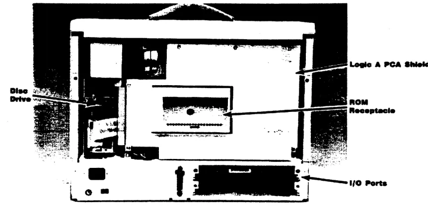
12V, -12V, +15V, and + 18V outputs.The major system assemblies and I/O devices are identified in figures 1-1, 1-2, and 1-3.
Prlnt.r _ _ _ _ _ _ _ ~
DI ... V
ROIl
Door
--- ~
Disc
...L __ --... ---
Driv.Figur. 1·1. Integral Personal Computer-Front View
#; ... .
~---~---~.-~-
..--'-~--.
~:.-.---,-•
,----.- ·---(·.1
I
.. ___ . ______ . ___ J
"P.,.---·o-.---~---
....
T
I:. ____________
:..!..J. ....----:!!t.
Int.., •• Peno ... 1
eo ...
uterDIM
Drtwa
·111·
L " •
•
Product Inform .. 101I 1·3
... APCA ...
ROM
R . . . ptecle
-1/0 Porta
Figure 1·3. Inte.raa Personal C~mputer-Int.,nal View
1 .3 Specifications
Detailed equipment specifications are shown in table 1-1. TIda •• 1-1. Specification a Physical Propertl . .
• Width: 425 mm (16.7 inches). • Height: 331 mm (13.0 inches). • Depth: 215 mm (8.5 inches), • Weight: 11.5 kg (25.3 pounds). CPU
• 68000 microprocessor (16 bit, 8 MHz).
RAM
• Memory mapped; four segments. • S12K-bytes internal RAM.
• Up to 1M-bytes external RAM. 110M
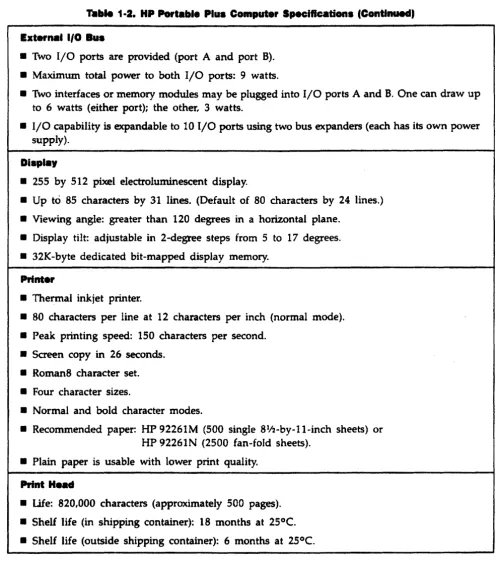
[image:12.611.118.549.57.265.2]Table 1·2. HP Portabl. Plus Computer Specifications (Continued)
Ixtern •• 1/0 aus
• Two I/O ports are provided (port A and port B). • Maximum total power to both I/O ports: 9 watts.
• lWo interfaces or memory modules may be plugged into I/O ports A and B. One can draw up to 6 watts (either port); the other, 3 watts.
• I/O capability is expandable to 10 I/O ports using two bus expanders (each has its own power supply).
Di.pt.,
• 255 by 512 pixel electroluminescent display.
• Up to 85 characters by 31 lines. (Default of 80 characters by 24 lines.) • Viewing angle: greater than 120 degrees in a horizontal plane.
• Display tilt: adjustable in 2-degree steps from 5 to 17 degrees. • 32K-byte dedicated bit-mapped display memory.
Prlnt.r
• Thermal ink jet printer.
• 80 characters per line at 12 characters per inch (normal mode). • Peak printing speed: 150 characters per second.
• Screen copy in 26 seconds. • Roman8 character set. • Four character sizes.
• Normal and bold character modes.
• Recommended paper: HP 92261M (500 single 81f2-by-l1-inch sheets) or HP 92261N (2500 fan-fold sheets).
• Plain paper is usable with lower print quality.
Print H •• d
[image:13.615.49.545.57.621.2]DISC DrIve
• 31!2-inch micro-floppy disc drive.
• Burst transfer rate: 62.SK-bytes
per
second. • Encoding: Modified Frequency Modulation. • Rotational speed: 600 revolutions per minute. • Capacity: 709K-byt~.• Bytes
per
sector: 512. • Sectors per track: 9.• Total tracks per surface: 80. • Available tracks per surface: 77. • Spare tracks per surface: 2. • Wear track per surface: 1. • Surfaces per disc: 2. • Interleave factor: 1.
Disc ...
• Life:
3x
106passes per
track. • Read errors: 1per
109 bits read.K.poa,..
• 90-key condensed ITF (Integrated Terminal Family) keyboard. • Detachable, low profile (30 mm high).
• Adjustable tilt, 0 or 8 degrees.
• Modified HP-HIL (Hewlett-Packard Human Interface Unk) keyboard interface with two HP-HIL connectors .
...
• Frequency range: 100 to 5000 Hz.
1IHI-1'IIII. Clock
• Accuracy: maximum error, 120 seconds per month; typical, 30 seconds per month. • Battery life: minimum expected, 6 years; typical, 12
years.
HP·18
Int."'.
1·8 Product InfOl'lll8tlon
,.. .... 1·2. HP PorbIIale Plus Computer SpeellClltlon (Continued. Invlronmental U ... a
• Computer: Operating temperature: 0° to 40°C (32° to 104°F). Storage temperature: -40° to 75°C (-400 to 167°F). Operating humidity: 5% to 95% RH at 40°C (104°F). Non ... operating humidity: 90% RH at 65°C (149°F). Operating altitude: 0 to 4600 m (0 to 15,000 feet). Non-operating altitude: 0 to 15,300 m (0 to 50,000 feet). • Disc media: Operating temperature: 10° to 40°C (50° to 104°F).
Long-term storage temperature: 10° to 60°C (50° to 140°F). Transporting temperature: - 40° to 60°C (- 40° to 140°F). Humidity: Sera to SO% RH at 40°C (104°F).
• Print Head: Operating temperature: 10° to 40°C (500 to 104°F). Storage temperature: -200 to 60°C (-4° to 140°F). Humidity: 5% to SO"o RH at 40°C (104 oF).
Power Requirements
• Volta.e, 87 to 127 Vac (115 Vac line). 195 to 264 Vac (230 Vac line). • Frequency: 47.5 to 66 Hz.
• Power: 88W.
1.4 Serial Number Information
The serial number of the computer is used for identification and the determination of warranty status. It is located on the safety label near the power cord receptacle. Its format is described below.
A
YYWWBXXXXX
--~
f
+ .... ---
Sequence number.10.
_ _ _ _ _ _ _ _ Location manufactured:
A: USA
B: Brazil
Q: United Kingdom S: Singapore
' - - - Week manufactured.
Chapter 2
Site Preparation and Requirements
Chapter 3
Installation and Configuration
3.1 Introduction
The Integral Personal Computer is a self-contained computer system, complete with printer and dis-play. Therefore, setting up the unit requires little time and is very simple. This chapter tells you how to set up the computer for use or in preparation for troubleshooting.
3.2 Preparation
CAUTION
Be sure the computer is set for the line voltage that you are using. Check the selector switch on the back panel near the power cable. Failure to do this can result in improper operation and/or possible damage to the computer.
1. Place the computer on a table with the back panel facing toward you.
2. Make sure that the line voltage switch on the back of the computer is set to the correct voltage (115 or 230 Vac).
3. Make sure that a good fuse of the proper rating is installed in the fuse receptacle on the back panel. A computer operating on 115 Vac requires a 1.SA fuse. A computer operating on 230 Vac
requires
an 800-mA fuse.4. Tum the computer around, so that the front now faces
you.
L Press the buttons on the two latches on the top cover and slide them toward the carrying handle. .. Lift up on the cover. It will swing up on its hinges.
7. Push the cover away from you. It will swing down along the back of the case. Make sure the keyboard doesn't fallout (don't open the printer lid until you remove the keyboard).
L lift the keyboard up and out of the front of the case, and place it on the table in front of the computer.
I. Plug the keyboard cable into either of the two HP-HIL jacks.
10. Plug an ac power ,cable into the receptacle on the back of the computer and into an ac outlet. 11. Install paper in the printer as follows: Open the printer lid. Pull the paper bail forward. Push the paper down into the slot between the printer mechanism and the case. Continue pushing the paper until it comes out in the front of the printer mechanism. Adjust the top of the first page to a position just above the bail arm, engage the sprocket pins in the paper holes, then lower the bail arm.
3·2 In ... ContI ...
12. Install the printhead in the printer carriage as follows: Press down on the latch lever to open the printhead carrier. Position the printbead in the carrier, then raise the latch lever to lock it in position.
CAunOM
Chapter 4
Preventive Maintenance
The Integral PC does not require any preventive maintenance. However, the following practices should be observed to avoid damage to the unit and to obtain best results:
• Remove the printhead (ink cartridge) whenever shipping or storing the unit. This prevents possible damage caused by ink leaking out of the cartridge. This is particularly important when the unit is to be shipped in an unpressurized aircraft cargo compartment.
• Always insert the shipping disc (HP part number 1535-4881) in the disc drive before shipping the computer. This prevents possible damage to the disc drive.
• Avoid leaving the unit on continuously for an extended period while not in use. This prevents unnecessary wear on the electroluminescent display.
• Use care when deaning the exterior of the unit, especially the display screen, to prevent scratching. The display saeen is made of clear plastic, and it is easily scratched or damaged. Use a clean, damp, soft cloth to dean the display screen and plastic case. You can dampen the cloth with a warm, mild soap solution jf necessary. Do not use petroleum distillates, acetone, methyl ethyl ketone, or other strong
cleaners.
Chapter
5
Functional Description
5.1 Introduction
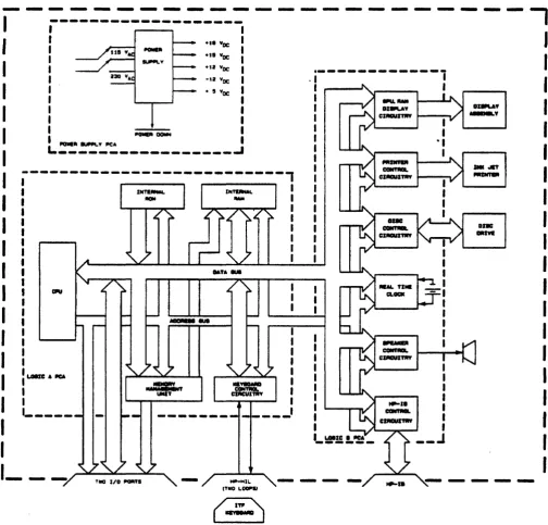
[image:22.612.69.573.214.697.2]This chapter describes the major components of the Integral Personal Computer. The block diagram of figure 5 ... 1 shows how the components of the computer are connected together and identifies the major printed circuit assemblies (PCAs).
---
---~---~-
---,
••• 'lac:
.1.
'lac:·,2 'lac:
-sa 'lac
• , 'lac:
IIQIIIEIli ~y JIC"
L_~
___
~__
~~______
~~-~---~---~---,
...
-
II I I
I
I I
I
___ I
..
_----_
...
_---,
I
I I I I I I I
__ J
The logic A PCA contains the computing electronics of the Int~ PC, including the CPU (central processing unit), RAM (random-access memory), and MMU (memory-management unit). The key-board controller and external I/O (input/output) logic circuitry are also located on the logic A PCA. The internal ROM (read-only memory) is contained in the plug-in ROM assembly, which plugs directly into the ROM receptacle on the logic A PCA.
The plug-in ROM assembly has room for two ROM PCAs: The operating system ROM PeA has four ROM Ies containing the HP-UX System V operating system. The option ROM PCA, if present, contains optional ROM-based software.
Note: H the computer is equipped with the earlier System m operating system, the plug-in ROM assembly has two PCAs containing the operating system. No optional ROM can be added to this assembly. The assembly cannot be serviced to the component level. It can only be exchanged.
The logic B PCA contains the control circuitry for the display, printer, disc drive, and speaker. The speaker itseH, the RTC (real-time clock), and the HP-IB (IEEE-488) interface are also located on the logic B PCA.
The I/O backplane PCA provides two I/O connectors (one each for I/O ports A and 8) and contains
no logic circuitry. .
The display assembly consists of an electroluminescent display panel, a display PCA, and the necessary mounting hardware. The display assembly is a tuned circuit. It cannot be serviced in the field. If the display assembly is bad, replace it.
The power supply provides voltages to the circuits of the computer as shown in table 5-1. 1"l1li •• 5-1.
Volta,.
Requlre ... ntsA ... bly
+IV +12V -t2V +1SV +18V
Logic A PCA X X X
Logic B PCA X X
Disc Drive X X
Display X X
Printer Mechanism X
Keyboard X
External I/O Bus X X X
Fan X
... c ...
pu . . , Funo ... DMcrIptions..a
5.2 CPU
The
CPu, Ie
U7 on the logic A PCA, is a 68000 HMOS (high-density metal-oxide semiconductor) microprocessor. The external clock frequency is 8 MHz.It performs the following functions:
• Controls circuit operations via the control bus according to programs stored in RAM and ROM.
• Directs the transfer of data on the physical address and data buses. • Responds to interrupts from both internal and external I/O.
The processor provides a 16M-byte addressing range that is divided among the internal and external ROM, the internal and external RAM, and the internal and external I/O as shown in table S-2.
Note. "Internal' refers to those components that are built into the system, including the ROM assembly that plugs into the logic A PCA. 'External" refers to those components that may be plugged into the external I/O ports.
,.. .... 1-2. Physical Add,...
".p
Addre . . Ra ....
U . .
...
,
0OOOOO-07FFFF Internal ROM (operating system peA): SI2K-bytes OSOOOO-OFFFFF Internal ROM (option ROM PCA): Sl2K-bytes
100000-4FFFFF External ROM modules: 4M-bytes
SOOOOO-SFFFFF Reserved: 1M-byte
6OOO00-6FFFFF Internal I/O: 1M-byte
700000-1FFFFF External I/O: 1M-byte
SOOOOO-EFFFFF External RAM modules: 1M-bytes
... ...,....1
Computer5.3 Interrupts
The CPU provides seven priority levels for hardware intenupts. The levels are encoded by U60 on the logic A PCA. The levels have been allocated as shown in table 5-3.
, . . . W. Interrupt Allocdons
Interrupt Level Interrupt SoUrce
(High priority) 7 Soft reset from keyboard (non-maskable) 6 Real-time clock or NBIR3 (external I/O) 5 Disc Drive or NBIR2 (external I/O) 4 GPU· or NBIRI (external I/O)
3 HP-m, printer, or NBIRO (external I/O)
2 HP-HIL devices (e.g. keyboard, mouse) (Low priority) 1 Real-time clock
• The graphics processing unit in the disp~ay interface.
The external I/O interrupt lines, NBIRO through NBIR3, can be asserted by an interface plugged into an external I/O port.
5.4 RAM
The computer contains 512I<-bytes of internal RAM arranged in a 256K by 16-bit configuration (ICs U20 through U35 on the logic A peA). In addition, a 1M-byte block of RAM address space is avail-able for external RAM modules. The RAM portion of the physical address space is shown in table 5-2.
5.5 ROM
The CPU allocates address space for up to 1M-byte of internal ROM (located in the plug-in ROM assembly). In addition, a 4M-byte block of address space is reserved for external ROM modules.
(Ex-ternal ROM modules would plug into the ex(Ex-ternal I/O ports. None are currently available.) The ROM portion of the physical address space is shown in table S-2.
5.5.1 The Plug-In ROM A ••
embly
All internal ROM is contained in the plug .. in ROM assembly, which plugs into the ROM receptacle on the logic A PCA. The HP-UX System V plug-in ROM assembly has room for two PCAs: the operating system ROM PCA and the option ROM PCA. A SI2K-byte block of ROM address space is reserved for the operating system ROM PCA, and ·a Sl2K-byte .block is reserved for the option ROM PCA.
Both PCAs can be serviced.
5.5.2 The ROM Bus
The CPU communicates with the internal ROM by means of the ROM bus. The bus is divided into three parts: the physical address bus, the data bus, and the control signals. The ROM bus connects the CPU to the plug-in ROM assembly by means of the ROM receptacle. Refer to table 10-2 for the ROM receptacle pin assignments.
TIt. ROM Ph,.1U1 Add,. ... (A1 Tltrougla A17J. The 17-bit unidirectional physical address bus is driven by the CPU. The 17 physical address bits correspond directly to logical address bits Al through A17 in the CPU. AO is a bit that distinguishes the upper byte from the lower byte in a 16-bit word. It is internal to the CPU and does not appear on the address bus .
... ROil DatIIlu. (DO Through D15J. The 16-bit bidirectional three-state data bus provides the gen-eral-purpose data path for the system. It can accept data in either word (16-bit) or byte (8-bit) length. The upper byte of the data bus includes 08 through 015; the lower byte includes DO through 07. The upper and lower bytes of a word are always enabled during an internal ROM access .
... ROM Control 51_I •• The ROM control signals include four ROM-select signals and RDTACK. The ROM-select signals are decoded by IC U19 on the logic A peA. Each of these signals (ROMO, ROMI, ROM2, and ROM3) selects a 256K-byte block of ROM address space in the plug-in ROM assembly. Table 5-4 shows the address range enabled by each ROM-select Signal.
Tala •• 5-4. ROII·SeI.ct Addre •• _ . . .
RO .. • . . . Slg .... Addr ...
ROMO 0OOOOO-03FFFF
ROMI 040000-07FFFF
ROM2 080000-0BFFFF
ROM3 OCOOOO-OFFFFF
ROTACK is the ROM data transfer acknowledge signal. This signal (by going low) indicates that the data transfer portion of a bus cycle is completed. When the mainframe recognizes RDTACK during a read cycle, data is latched and the bus cycle is terminated.
5.8 MMU
The MMU (Memory-Management Unit) consists of a 4 by 12-bit register file (ICs U55 through US7) and a 12-bit full adder (ICs U47 through U49), all mounted on the logic A PCA. Its function is to perform address mapping.
5.6.1 Address Mapping
Mapping is performed during RAM operations only; that is, when the most significant bit of the phys-ical address (PAl3) is high.
1·8 Functlo_1 Description Int ... P.,...I
eo ...
ut_The register used for the mapping function is selected by the FCI and FC2 (function code) bits from the CPU.
The MMU is a write-only device that powers up into an unknown state. It must be initialized before any RAM accesses are attempted.
5.8.2 Physical
Addr.s.
Bit 23
Physical address bit 23 (PA23) distinguishes mapped RAM accesses from unmapped ROM or I/O accesses. It is high during a RAM access and low during a ROM or I/O access.
PAl3 is derived (by IC U43 on the logic A peA) from the CPU logical address bit A23 and function code bit PC2.
5. 7 Internal 1/0
Internal I/O devices are those devices that are built into the computer system. The keyboard control
circuitry and MMU are located on the logic A PCA. The real-time dock, HP-IB interface, and speaker. are located on the logic B peA, along with the control circuitry for the disc drive, display, and printer.
5.7.1
Interne.
1/0
Addressing
The internal I/O physical address map is shown in table 5-5. Each device is allocated a 64K-byte block of address space.
,.. .... 5-1. Int.' ....
110
Ph,.tal Addre . . lI.p Ad . . . n . .Port Num ... ,
Uu
(H.ndeoi ... )
600000-60FFFF 0 MMU
610000-61FFFF 1 Disc Drive
620000-62FFFF 2 Display
630000-63FFFF 3 HP-IB
640000-64FFFF 4 Real .. Time Clock
650000-65FFFF 5 Printer
660000-66FFFF 6 Keyboard
670000-67FFFF 7 Speaker
680000-68FFFF 8 Reserved
690000-69FFFF 9 Reserved
6AOOOO-6AFFFF 10 Reserved
6BOOOO-6BFFFF 11 Reserved
6COOOO-6CFFFF 12 Reserved
6DOOOO-6DFFFF 13 Reserved
6EOOOO-6EFFFF 14 Reserved
.. unci ... DeeorIpUon .. 7
5.7.2 The Logic A to Logic
a aus
The logic A to logic B bus provides the communication path between the two logic boards. The bus can be divided into three parts: the physical address bus, the data bus, and the control signals. Table 10-3 gives the connector pin assignments for the logic A to logic B bus.
The Logic A-8 Ph,s'" Acid,... Ba. C.8A t Through 'BAS). This is a unidirectional five-bit bus driven by IC U6 on the logic A PCA. The five physical address bits correspond directly to the At
through A5 logical address bits in the CPU. IBAS is the most significant bit of the address.
The Logic A-B DIIUI Bu. C.8DO Through 'BD7). This is a bidirectional eight-bit bus driven by IC US on the logic A PCA. IB07 is the most significant bit of the bus.
!!!!..-
Logic A-!E.!..ntrol ... These ~als include: RO, WR, SPKWR, HPm, RTC, RESET, PRNT, DISP, DISC, PWRDN, IRl, and IR3 through IR6. All of these signals, except PWRDN, are active low.The read (RD) and write (WR) signals define the data bus transfer as a read cycle or a write cycle. If RD is low, the transfer is a read cycle. If WR is low, the transfer is a write cycle. Only one of these two,
signals can be low at a time.
The device-select signals (SPKWR, HPIB, RTC, PRNT, DISP, and DISC) correspond to the six internal I/O devices on the logic B PCA. They are generated by les U3, U13, and UI0 on the logic A PCA, and are described in table 5-6 .
...
DescriptionSPKWR Speaker (qualified by WR)
HPIB HP-IB
RTC Real-time clock
PRNT Printer
DISP Display
... .unoll_1 "'ecriptlon I ... C ... '
Each device-select signal corresponds to a 64K-byte block of address space as shown in table 5-5. The RESET signal is driven low for at least 100 ms after the power is turned on. RESET also goes low a minimum of 100 ms starting at least 1 ms before system power is lost. The RESET signal is driven low for 15.5 lIS in response to a RESET instruction.
The PWRDN (power down) signal originates as PWRDN on the
power
supply PCA (PWRON isbuff-ered and inverted). The PWRDN signal holds the RESET output low for at least 100 ms when the power is turned on. The PWRDN signal provides an early warning to the computer of loss of power. The interrupt request signals (IRI and 1R3 through IR6) are used by the internal I/O devices to request interrupts at five different levels. Refer to section· 5.3 for the interrupt assignments.
5.8 External 1/0
An external I/O device is an interface or memory module plugged into one of the two ports in the I/O backplane of the computer or into a bus expander port. These devices are linked to the CPU by the external I/O bus.
5.8.1 External 1/0 Addressing
The external I/O physical address map is shown in table 5-7. Each device is allocated a 64K-byte block of address space.
,....1.1-7. aXl ... 110 .... ysicIIl Add,... Map Add ... R _
Port M.nlb_
U
••
,
...
,
700000-70FFFF 16 Mainframe Port A
710000-71FFFF 17 Mainframe Port B
720000-72FFFF 18 Bus Expander Port Al
730000-73FFFF 19 Bus Expander Port A2
740000-74FFFF 20 Bus Expander Port A3
7S0000-7SFFFF 21 Bus Expander Port A4
760000-76FFFF 22 Bus Expander Port AS
770000-77FFFF 23 Reserved
7S0000-7SFFFF 24 Reserved
790000-79FFFF 25 Reserved
7 AOOOO-7 AFFFF 26 Bus Expander Port Bl
7BOOO0-7BFFFF 27 Bus Expander Port B2
7COOOO-7CFFFF 28 Bus Expander Port B3
.
7DOOOO-7DFFFF 29 Bus Expander Port B4
7EOOOO-7EFFFF 30 Bus Expander Port B5
...
~ . II ... DMGrIpIIon . . .... Memory modules are initially addressed using the appropriate port address. However, once configured, they are addressed outside the·port selected' address space. Table 5-2 shows the address space reserved for external memory modules.
Figure 5-2 shows the locations of the I/O ports for the Integral PC and two HP 82904A Bus Expanders.
A1
I
A3A2
I
A4 Bus Expander.-.
ASComputer
91
I
B3I
A 92I
B485.
I
B-
.~Bus Expander
. . . 1-1. 1/0 Port . . . .
aon.
1.8.2
Til. Ext.mal
1/0
Bus
The external I/O bus provides the link between the CPU and the external I/O devices plugged into the I/O backplane. The bus can be divided into three parts: the physical address bus, the data bus, and the control signals.
The Ixt .... IIIO Ph,,,1 Add,. ... laA t Throug" BAD). This bus is 23 bits wide and is latched by les U44, U4S, and U46 on the logic A PCA. BA23 is the most significant bit. The least significant bit (AO), which distinguishes the upper byte from the lower byte in a 16-bit word, is not present on the bus. In its place two signals, NBUD and NBLD, are prOvided. They specify whether the upper byte, lower byte, or both bytes of the addressed word are involved in a cycle.
TIl. Ixterull/O D . . .
au.
,BDO Through BD11). This is a 16-bit bidirectional bus driven by ICs U53 and US4 on the logic A PCA. The upper (even) byte of the bus 'consists of BDS through BOIS. The lower (odd) byte of the bus consists of BDO through BD7.The 1&1 ... 11/0 Control ... These signals include: BR/NW, NBUD, NBLO, NPSO, NPSI, NBAS, NBIMA, NBDTACJ(, NBRESET, NBIRO through NBIR3, NBDMARQ, GRIN, and GROUT. Ex-cept for GRIN and GROUT, all of these signals are active low.
BR/NW is the read/not write signal. This Signal, when high, indicates a read cycle; when low, it indicates a write cycle on the data bus.
.. 10
'unell_.
De8Ol'lption... c ... '
NPSO and NPSI are the port select signals for ports A and B, respectively. The NPSO or NPSI signal indicates to a card that it is being accessed within its 'port selected' address space. The signal, when low, indicates that BAI through BA23, BR/NW, NBUD, and NBLO are valid for the selected port. NBAS is the address strobe signal. This signal, when low, indicates that BAI through BA23 and BR/NW are valid. The address strobe signal is used by memory modules since they must be accessed outside the 'port selected' address space for the I/O port.
NBIMA is the 'I'm addressed' signal. A memory module uses this signal to indicate (by a low signal) that it has been previously allocated the address specified by the current bus cycle.
NBDTACK is the data transfer acknowledge signal. This signal (by going low) indicates that the data transfer portion of a bus cycle is completed. When the mainframe recognizes NBDTACK during a read cycle, data is latched and the bus cycle is terminated. When NBDTACK is recognized during a write cycle, data' is removed from the bus and the cycle is terminated.
NBRESET is the reset signal. This signal goes low for at least 100 ms when the power is turned on. It also goes low for at least 100 ms starting a minimum of 1 ms before the power goes off. The NBRESET signal goes low for 15.5 IJ.S in response to the RESET instruction.
NBIRO, NBIR1, NBIR2, and NBIR3 are the interrupt request signals. Interfaces assert these lines low to request asynchronous interrupts at different interrupt levels. External interrupt request levels NBIRO through NBIR3 correspond to internal interrupt request levels IR3 through IR61 respectively.
NBDMARQ is the direct memory access request signal. The Integral PC does not support direct mem-ory access. The NBDMARQ pins on the port A and port B connectors are wired together to facilitate
bus expander testing.
GRIN and GROUT
are
not used by the Integral PC. In the I/O port connectors the GRIN pins are tied low, and the GROUT pins are left open.1.8.3 The
1/0
Backplane
The I/O backplane assembly provides the link between external I/O devices and the external I/O bus. It consists of the I/O backplane peA and a guide asse~bly to hold interfaces and memory modules. The I/O backplane peA has two connectors, one for port A and one for port B.
The I/O backplane assembly can support a total power requirement of 9 watts for both ports. An individual port can support a 6-watt power requirement. Thus, up to one 6-watt interface and one 3-watt interface (or memory module) may be installed.
Notel You can expand the I/O capability of the Integral PC to 10 ports by using two bus expanders as shown in figure 5-2. Each bus expander has its own power supply.
Punctionlll DHCI'lption 1·11
5.9 Display
The Integral pe uses a
255
by 512-pixel electroluminescent panel display. Thedisplay
controller
is located on the logic B PCA. The electroluminescent panel and its associated driver circuitry are locatedin the
display assembly.
Figure 5-3 is the display block diagram.r-~----~---~---~--~--~---,
I I
I MEMORY I
CQNTACIL
---.
I LOGIC II 1U2. UIi-il. usal I
I I
~ I
I I I
I I~
~
DISPLAY MEMORY I(U3-e. I
:<
l/1
:>
ISYSTEM
~:
8RAPHICS ICDNTAOL. PRJCESSINfi
~
IUNIT
~I
IV
CUll I~}
I•
I I I
I I
LOGIC A PCA I I
---
DATA I~
DISPLAYSHIFTER
V
ASS08LY(U7. U8)
:
DATA au! I
I
I
AIXIAISS IUS TlMING I AND I
SYNC I
• CONTROL Laale. PCA CIRCUITS cue. UIO. Uilll I
I
. - - - .. ~--,..---~----~~-... - ... _____ I '1 . . . . W. Dis,,,, Block Diagram
1.1.1 The
Display Controll.r
The display controller consists of the following components:
• The GPU (graphics processing unit) miaoprocessor. This miaoprocessor (Ie U1 on the logic B peA) is specially designed as a display controiler.
• The display memory. This is a 32K-byte memory organized as a 16K by 16-bit bank of dynamic RAM (lCs U3 through U6 on the logic B peA).
• The control logic for the display memory (ICs U2, U11, U12, U13, and U16 on the logic B peA). • The data shifter (ICs U7 and U8 on the logic B PCA), which consists of tWo 8-bit shift registers that
convert the outgoing data to serial form.
1-1
a
lIunction . . . crlptlonThe display controller outputs data to the display assembly. It performs a complete display refresh cycle
60 times a second in order to keep the image visible on the display saeen. The display refresh process is accomplished using line-at-a-time scanning. In this process, which differs from the dot-at-a-time raster scan process used in CRT monitors, an entire 512-pixel display line is activated at one time. The GPU controls the storing of data in display memory, and the reading of data for output to the display assembly. The GPU also controls the timing and sync (synchronization) circuits, which output the sync signals to control the display assembly.
The display memory stores data in a bit-mapped format. For each point on the display screen there is a corresponding bit in the display memory. If the bit in the display memory is a -I', the corresponding point on the screen will be lit; if the bit is a '0', the point will be dark.
The GPU performs display memory cycles continuously, but only every other cycle is a display refresh cycle. The GPU uses the alternate memory cycles to modify and manage the contents of the display memory.
The GPU performs the refresh process by reading sequential locations in display memory and sending the information stored in those locations to the display assembly. However, the GPU transfers the data to the data shifter one 16-bit word at a time. The data shifter consists of two 8-bit shift registers, one for the odd bits and one for the even bits of each word. When these shift registers are fully loaded, they send the data in serial form two bits at a time (odd and even bits) to the display assembly.
At the display assembly the incoming bits are entered into two 256-bit shift registers. When the shift registers are full, the 512 data bits are latched, and the display drivers are activated for the entire line. Thus, the desired pixels in the selected. line are turned on. This process is repeated until each of the 255 lines have been written. The refresh process then begins again at the top of the screen.
Notel The System
m
operating system provides a display timeout feature. If a unit is equipped with System Ill, its display normally times out after 15 minutes of unattended oper-ation. (The display comes back on when you press any key.) You can disable the timeout feature with the d i sp_ t i me_o f f command on the Utilities disc. The System V operating system does not implement the display timeout feature.5.8.2 The
Display A.sembly
The display assembly consists of a 512-pixel by 255-line electroluminescent panel and the associated driver circuitry and mounting hardware. The display assembly is a tuned assembly. It cannot be serviced in the field. If this assembly is faulty, replace it.
5.1 0 Keyboard
The detachable keyboard is a compressed ITF (Integrated Terminal Family) keyboard. It contains S'O keys, including cursor keys, edit keys, a numeric pad, and eight function keys. Autorepeat and n-key rollover functions are provided.
Fu ...
a. ....
ptlo.. ..13An HP-HIL (Hewlett-Packard Human Interface link) keybotqd interface, IC US8 on the logic A PeA, controls the keyboard. The keyboard plugs into either one of the two HP-HIL jades on the front panel (lower left) of the computer.
The number of HP-HIL devices (for example, a keyboard and mouse) that can connected to the rom-puter depends upon the
power
drawn by the individual devices. (The Integral PC keyboard draws 100mA)
The totlll power drtnDn
byall HP-HIL devices connected to the
twojacks must not aceed
600 mAoThe HP-HIL controller can configure up to seven devices if they do not exceed the power rating.
5.11 Disc Drive
and Controller
The Integral PC includes a double-sided 3Y2-inch miaofloppy disc drive. The disc control circuitry includes a Western Digital 2797 floppy disc controller IC (Ut8 on the logic B PCA) and associated logic circuitry. Figure 5-4 is a block diagram of the disc drive and controller.
---,
1---.
I I
1 I
~ ______ ~I ____ ~ I
SVSTEM CONTAOL
I I I I I I
DISC
CaNTADLLE
(Ull.,
I LOGIC 8 PeA •
---~---~
FI .... 5-4. Disc Drive Block D ...
DISC DAIVE
- - . - . . CDNTAOL CIRCUITS
The disc drive routine resides in operating system ROM. It contains a software loop to control data transfer.
The disc drive uses double-density recording in accordance with the Hewlett-Packard MFM (modified frequency modulation) format.
Each disc drive assembly consists of a drive mechanism, a read/write head, a head· positioning mecha-nism, the control interlocks, and a PCA containing the electronic components. The read and write circuits, the head-position control circuit, and the read, write, and erase enable circuits are all located on the disc drive peA.
1-14 FunctiOlUll Deaorlptlon Ine..,.. ... Computer
5.12 Printer
The Integral PC includes an 80-column dot matrix inkjet printer that uses a disposable printhead. (The printer is a modified ThinkJet HP-IL printer.) Figure 5-5 is the printer block diagram.
r---,
I
I I
I I
I I
I I
I I
I I
IYITDI
coma..
t---',
HEAD DOTI
MOTOR CONTROL
.---....---. I
PRINT!JII
"eM.
I HOME AND OUT -OF ·P"'PEA DETECT
I
~ LOGIC A PCA I - - - ______ 1
Laale • PCA
I~ _____
---~----===> ...
- - - CCIITROL CIRCUITS
p .. ..,. 1-1. Printer Block
Dla.ram
The printer uses an HP-IL interface (U31 on the logic B peA) to communicate with the computer. It
has a custom-designed controller IC (U28 on the logic B PCA), a lK-byte RAM
Ie
(U27 on the logic B PCA), and a 16K-byte ROM IC (U32 on the logic B PCA).· The lK-byte RAM IC buffers at least one line of 12 by 640 dot graphics. The 16K-byte ROMIe
contains the character font table.The control panel includes a form-feed key, a line-feed key, and a continue-operation key that is used to set the top-of-form position and to recover from errors. The panel includes an attention light (the yellow LED) that comes on continuously to indicate an out-of-paper condition and blinks to indicate an error condition.
The printer provides printing and non -printing self tests to identify failures.
5.13 Real· Time Clock
The real-time dock (located on the logic B PCA) keeps time continuously, even while the computer is turned off. The clock also provides the timing for the operating system.
The clock controller (Ie U44 on the logic B PCA) is a National Semiconductor NS58167 A IC that counts from 1/10,000 second to months. It contains two interrupt outputs. The STANDBY INT output interrupts at interrupt level 6 when the clock count matches a predetermined value (user
programma-ble). The INT output interrupts at interrupt level 1 either when a predetermined value is matched or at a predetermined periodic interval (also user programmable).The 32.768-kHz oscillator (Yl on the logic B PCA) can be fine tuned by adjusting the variable capac-itor (C43 on the logic B PCA) connected to pin 10 of the controller Ie.
The oscillator is connected to an LM 358 operational amplifier (U40 ~n the logic B peA). The opera-tional amplifier is wired in voltage-follower configuration to buffer the clock signal. The buffered dock signal is available at test point TPl for measurement with a frequency counter.
The standby lithium battery (BTl on the logic B PCA) maintains clock operation while the computer is turned off. The battery has a six-year minimum expected life (12 years typical).
Each of the controller address and control lines is connected to ground through a 22-kO resistor (R38
on the logic B peA). This prevents the inputs from floating into their linear operating regions when the computer is turned off, reducing the drain on the standby battery.
5.14 Speaker
The speaker (LSI on the logic B PCA) allows the user to generate tones in the range 100 Hz to 5000 Hz.
The speaker controller (Ie U39 on the logic B peA) is a National Semiconductor COP 452 frequency generator/counter. The controller outputs a square wave, the frequency and number of pulses of which are programmable.
5.15 HP-IB Interface
The computer contains an HP·IB (Hewlett-Packard Interface Bus) interface that is compatible with the
1EEE-488 standard. It is the primary means for interfacing the computer to peripherals such as plot-ters, external prinplot-ters, and external disc drives. The HP-IB interface is also often used for data acquisition and controller applications.
The interface circuit includes two bus transceivers: an SN 75160A (Ie U42) and an SN 75162A (Ie U43). It also includes a 9914 talker/listener/controller Ie (IC U41). An ALSOO quad-NAND IC (Ie U26) provides for the decoding of the controller:enable signal. All of these components are located on the logic B PCA.
Jumper WI defines whether the interface is to be system controller of the HP-IB or not. It is fadory set in the system controller position since the interface is most often used in this mode.
5-t 8 Functlona. Desortptlon
5.16 Power
Supply
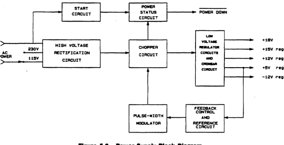
The Integral PC power supply is an off-line switcher. It is located on a separate printed-circuit assem-bly. Figure 5-6 is a block diagram of this circuit.
START POWER
CIRCUIT STATUS POWER DONN CIRCUIT
[image:37.615.60.544.132.380.2]LOW
... YGLTMIE Hay
PO
,
HIGH VOLTAGECHOPPER . . . TCIIII nov
AC RECTIFICATION CIRCUIT CIRCUITS WEFt
... uev CIRCUIT AND
H5Y rev.
+t2V ,.ea.
, ~
CIRCUIT +ey rea.
-12v reg.
FEEDBACK CONTROL PULSE-WIOTH AND
MOOUl.ATOR REFERENCE CIRCUIT
Figure.... POW., Supply Block D ... ,. ..
The power supply provides five direct-current outputs. The +SV, + 12V, + ISV, and -12V outputs are regulated, and the + 18V output is not regulated. Table 5-1 shows which components of the com-puter use these voltages.
The following paragraphs describe the operation of the power supply. Refer to the schematic diagram in figure 12-11 to identify the components.
The 115 or 230 Vac line voltage is rectified by diode CR36 and applied to transformer Tt. Transistor Q3 chops the voltage at a frequency of 4S kHz. The appropriate voltages appear across the secondary windings of Tl and are rectified and regulated as required.
The pulse-width modulator (IC U4) controls the frequency at which the input to T1 is chopped.
Dur-ing normal operation power for modulator U4 is provided by the de voltage developed across capacitor CIl. However, since no voltage exists across Cl3 when the power is turned on, U4 remains turned off, and the power supply remains inoperative. To initiate operation, the start-up circuit
pro-vides power to U4.
Comparator UlO monitors the +5V output and feeds a signal back to modulator U4 (through optoisolator US) to control the frequency of the chopping circuit. If the
+
SV output should rise to 6.2V, transistor Q8 is turned on. This shorts out the+
SV output, and also shorts out the feedback signal through diodes CR27, CR28, and CR29, thereby turning off U4 and shutting down the power supply.Comparator U2A monitors the rectified line voltage. If the power starts to shut down and falls to a certain level, U2A turns on the POWER DOWN signal and warns the rest of the system before the
power
is lost completely. This allows the system to perform certain functions, such as preparing. the real-time clock for power shut-down .Chapter 6
Removal and Replacement
8.1 Introduction
This chapter desaibes the procedures for removing and replacing the assemblies and components of the Integral PC. To reassemble the computer,
you
will generally reverse the disassembly procedure. ~eassembly notes' are included in the procedures where additional reassembly information is needed. The directions 'left, .. 'right,' 'front,. 'back/ 'top,' and "ottom' in these instructions refer to the com-puter in the upright position as seen from the front (display side).6.2 Safety
Considerations
_IIIIING
Life threatening voltages are present in the power supply primary circuitry whenever the line corel is plugged in, even while the fH1UJtT switch is turntd off. Use extreme care whenever servicing the computer with the power supply cover removed. Electrical and mechanical failures may cause dangerous voltages to be present at points that normally are safe.
Observe the folloWing safety guidelines when working on the computer.
• Do all possible operations with the computer turned off.
• NtfJer work alone. Be familiar with the location of power switches in your service area and what they control.
• In case of an accident, know where to obtain respiratory resuscitation and cardiopulmonary resus-citation (CPR).
• Keep your work area neat and free of nonessential conducting material and sharp objects. Remem-ber that reaction to an electrical shock can cause you to strike nearby objects, possibly resulting in serious injury.
• Do not exceed the rated specifications of test instruments. • Observe all cautions and warnings in this manual.
8.3 ESD
Considerations
CAUTION
.. 2 ReMoval and ... I_ ... nt
I_,a' ...
eo ...
uterObserve the the following anti-static guidelines when working on the Integral PC:
• Use a static-safe workstation. At a repair bench, this may consist of a grounded anti-static work surface (an anti-static mat), a grounded wrist strap, a grounded soldering iron, and an ionized air blower directed over the workstation. At an on-site location, this may consist of a folding anti-static mat, a grounded cable, and a wrist strap. Keep all insulators (such as coffee cups, paperwork, or packing material) far away from static-sensitive devices. They are notorious static generators. . • Keep all assemblies and components in their conductive packages until needed. When the part is
needed, unpack it only at a static-safe workstation and only while you are grounded. If you must set the part somewhere, place it only on the conductive mat.
• Handle PC boards by the edges. Do not touch any component, trace, or connector.
• Keep your clothing away from static-sensitive parts, even when using heel and wrist straps. The static charge on clothing often is not bled away.
• Do not use erasers to clean contacts (they generate lotS of static and also tend to rub off the gold). • Connect the chassis of the instrument you are working on to the grounded mat so that it will
remain grounded even when you remove the power cord for service. The ground jumper should have a I-MO resistor built into it. to protect you in case of a ground fault in the instrument.
WAIINING
An anti-static wrist strap should have a I-MQ series resistor built into the ground jumper to protect you against an electrical shock through the wrist strap. Use of an unapproved wrist strap could result in a potentially fatal electric shock.
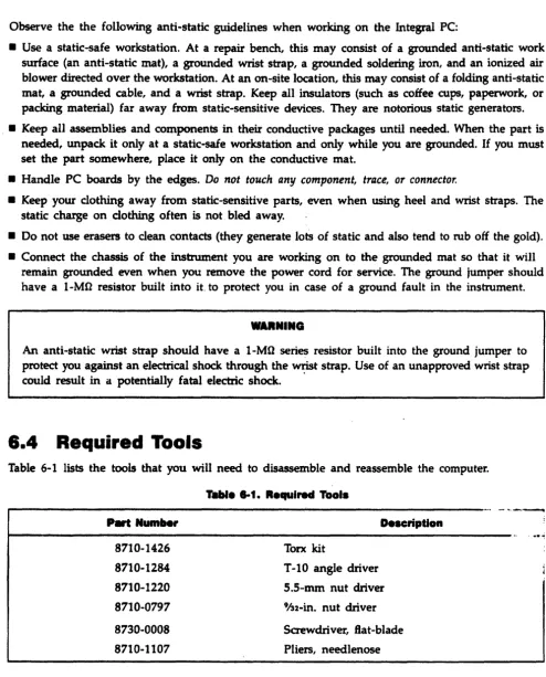
6.4 Required Tools
Table 6-1 lists the tools that you will need to disassemble and reassemble the computer. Table I-t. R.qulred Tools
,..---_
..-
,._-P~Num ... r 8710-1426 8710-1284 8710-1220 8710-0797 8730-0008 8710-1107
Description
Torx kit
T-IO angle driver S.S-mm nut driver 'In-in. nut driver Saewdriver, flat-blade Pliers, needlenose
[image:41.617.47.542.35.648.2]• • - . . . _ . . . . . , • • • ~.'WW
8.5 Removing the Back Case
To gain access to the assemblies and wiring inside the computer, do the following:
1. Open the computer by pressing the buttons and then sliding the two latches on the lid inwards towards the handle; lift the lid up, and swing it back on its rockers. Be careful that the keyboard assembly doesn't fall out. Remove the keyboard assembly.
•••
G •. t:i~.:: ...,-~~-- :~·~~;ri;\:::;~· ','
, ,','
,·l''ii~r}~·.
", ".. ',,- .. {~k},.\I!pjiA .../JJ}:;t .. );t
-~
't_---_-_ -_
-.:---1--..!f .
... ,. 6-1. Back Ca . . Sc,. . .
2. Swing the lid back up on top. Using a T-20 Torx driver, remove the screws on the sides of the back case. Tip the computer toward its front, disengage the back case from the top of the com-puter, then lower the back case to release its bottom lip. Remove the back case from the computer.
6.6 Removing the Lid
To remove the lid assembly:
. 1. Open the computer by pressing the buttons and then sliding the two latches on the lid inwards towards the handle; lift the lid up, and swing it back on its rockers. Be careful that the keyboard assembly doesn't fallout. Remove the keyboard assembly.
... Remova. and Replacement Integ,a. Per . . n •• Computer
3. Using needlenose pliers or a small screwdriver, remove the E-rings from the two small rocker pins
(see figure 6-2). Be careful not to drop the E-rings inside the case.
4. Disengage the bail arm from the pins and lift off the lid. Remove the spring washers from the rocker pins to prevent loss.
Figure 1·2. Computer-Lid Rocker
If you need to disassemble the lid, see figure 9-6.
6.7 Removing the Logic A peA
To remove the logic A peA, follow these steps:
1. Remove the plug-in ROM assembly if one is installed (refer to section 6.16.1).
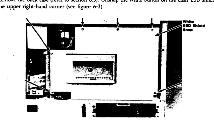
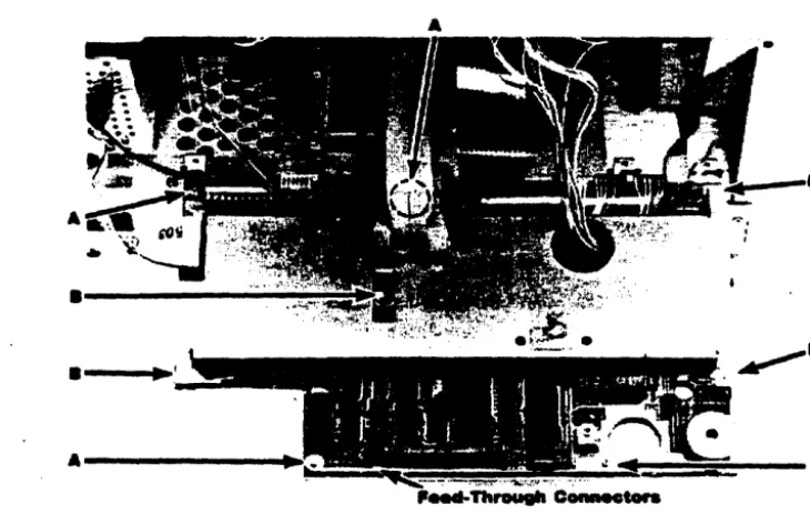
2. Remove the back case (refer to section 6.5). Unsnap the white button on the clear ESD shield in the upper right-hand corner (see figure 6-3). .
•
••
I
[image:43.612.66.487.87.402.2] [image:43.612.82.520.481.730.2]l ... r.I ... IC~ ... ." ... p l . . . . . .
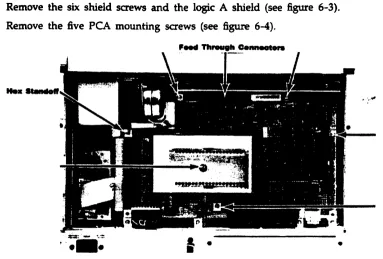
3. Remove the six shield screws and the logic A shield (see figure 6-3). 4. Remove the five peA mounting screws (see figure 6-4) .
...
• ',.'tII~:' .... '~.';t:.
•••••
I ·
•
Fig . . 1-4. Logic A peA Mounting Scre.s .nd Feed· Through Connector
Sa Use a S.S-mm nutdriver to remove the hex standoff (figure 6-4). The PCA is now held in place by the pins' in the feed-through connectors .
.. Grasping the peA at each side near the top, gently pull it out. Be careful not to bend the pins on the feed-through connectors.
7. Disconnect all cables from the bottom of the PCA. (Note that the large I/O cable connector has a locking lever on each side.)
L Remove the plastic insulator sheet.
Not.: If necessary, you can remove the ROM guide by disengaging, one at a time, the two tabs that are inserted in the slots in the PCA. Do not install the ROM assembly with the ROM guide removed. If you do, you will not be able the remove the ROM assembly.
R ... bl' Not • • To replace the logic A peA, follow these steps:
1. Insert both feed-through connectors in the logic B PCA (if they are not already there).
CAUTION
Make sure that you do not interchange the power-cable connectors to the logic A and logic B
peAs. The logic B power-cable connector is the one from which the disc-drive extension cable extends (see figure 6-32). If you interchange the logic A and logic B power-cable connectors, serious damage to the power supply or the logic peAs will result.
[image:44.612.83.467.55.314.2]3. While holding the logic A PCA with one hand, place the insulator sheet on the PCA mounting panel behind the PCA. Make sure the holes line up properly.
4. Carefully align the logic A PCA over the feed-through connectors and press the PCA into place.
Press as close to the connector as possible.
S. Replace the top two peA mounting screws first to hold the insulator sheet and peA in place, then replace the other screws and the hex standoff.
.. Reinstall the logic A shield, snap the white ESD shield button in place, then reassemble the unit.
6.8 Removing the Logic B peA
To remove the logic 8 peA, follow these steps:
1. Remove the back case (refer to section 6.5). Unsnap the white button on the clear ESD shield in the upper right-hand corner (see figure 6 .. 3).
2. Remove the six screws holding the logic A shield (see figure 6-3) and remove the shield. (Leave the logic A peA in place.)
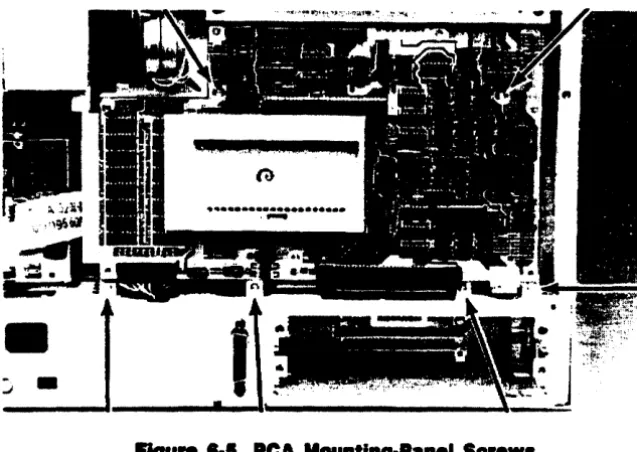
[image:45.615.125.444.328.554.2]3. Remove the six screws holding the PCA mounting panel (see figure 6-5).
FIgure 8-1. PeA Mounting-Pane. Screws
4. TIlt the panel down and toward you (unhook the cable dip from the printer-mechanism cables). Support the panel to prevent any strain on the cables.
.. There are four printer-mechanism cables that pass through the grommeted hole in the shield (see
figure
6-6). Disconnect these cables from the logic B PCA, but don't remove them from the grommeted hole....r. .... Grommeted Hoi. In Logic • Shield
7. Remove the four shield saews (labeled MB' in
figure
6-7). Lift up the shield and disconnect the display flex cable from the logic B peA.A
A
.---~~~
.-~~
'1 . . . 1·7. Logic • peA Screws and , . . d· Through Connectors.
.... ... ov . . . nd ... ~ Int ... ICom ...
I. Disconnect the remaining cables from the logic B PCA (the disc drive flex cable, power cable, printer switch-panel cable, and HP-IB ribbon cable).
Note: If the logic A PCA is still installed, its cables will hold the PCA mounting-panel assem-bly in place.; If the logic A PCA has been removed (or if you disconnect its cables), you can remove the PCA mounting-panel assembly and lay it on a bench.
10. Remove the four remaining screws that hold the logic B PCA (labeled MA" in figure 6-7). 11. The feed-through connectors now are all that hold the PCA. Grasp the PCA as near to the
con-. nectars as possible and gently pull the peA loose. Be careful not to bend the pins on the feed-through connectors.
12. Remove the plastic insulator sheet.
Re ... bIy Notes: Make sure the plastic insulator sheet is positioned properly relative to the screw holes in the PCA mounting panel. Insert the feed-through connectors into the logic A peA, align the logic B PCA over the pins, then press the PCA into place.
Press as close to the connectors as possible.
Secure the PCA with its mounting screws (labeled III A" in figure 6-7) before you reconnect any cables.CAUTION
Make sure that you do not interchange the power-cable connectors to the logic A and logic B PCAs. The logic B power-cable connector is the one from which the disc-drive extension cable extends (see figure 6-32). If you interchange the logic A and logic B power-cable connectors, serious damage to the power supply or the logic peAs will result.
Connect the display flex cable to the PCA before you reinstall the shield on the PCA. Figure 6-8 shows the proper orientation.
•
•
- . I i ' .-_ -.- - . . .' - ,;,.-., .. u
- ~---- - ---
--_
...-
..
--When you reconnect the four printer-mechanism connectors to the logic B PCA, make sure that the printer cables are properly oriented. The connectors are keyed. Install them as shown in figure 6-6.
Be sure that the printer cables are pulled tightly through the grommeted hole in the shield. The wires as they come out of the connectors in the open space below the shield must lie flat on the peA so as not to interfere with the fan (see figure 6-6).
Make sure that all cable connectors have been reinstalled before you reassemble the unit. Note: The printer ROM Ie (U32 on the logic B PCA) is localized for some languages. It is socketed for easy removal. Currently the standard version is used for all languages except Arabic, Hebrew, and Japanese. The standard printer ROM is supplied on all replacement logic B peAs. If you are replacing the logic B PCA on a unit localized for Arabic, Hebrew, or Japanese, remove the localized printer ROM from the defective PCA and install it in the re-placement peA. Install the standard printer ROM in the peA to be exchanged. If the printer ROM needs to be replaced, use the correct part number for the localized unit (refer to table 9-12).
6.9 The Printer Assembly
The printer assembly is a modified HP-IL version of the ThinkJet printer. Before you service the printer mechanism, remove it from the computer.
6.9.1 Removing the Printer
To remove the printer assembly, follow these steps:
1. Open the computer by pressing the buttons and then sliding the two latches on the lid inwards towards the handle; lift the lid up, and swing it back on its rockers. Be careful that the keyboard assembly doesn't fallout. Remove the keyboard assembly.
2. Open the printer cover. Remove the cpver as follows: bend the middle of the hinged edge out-ward slightly, then disengage the hinge pins. (See figure 6-9.)
Integra' Pen.nal Computer
3. Remove the back case of the computer (refer to section 6.5). Unsnap the white button on the clear
ESD shield in the upper right-hand corner (see figure 6-3).
4. Remove the six saews holding the logic A shield (see figure 6-3) and remove the shield. (Leave . the logic A PCA in place.)
S. Remove the six screws hol~g the peA mounting panel (see figure 6-5) .
.. Tilt the panel down and toward you (unhook the cable clip from the printer-mechanism cables). Support the panel to prevent any strain on the cables.
7. Disconnect the four printer-mechanism cables from the logic B PCA.
I. Remove the four screws that hold the logic B shield (labeled *B' in figure 6-7). Lift up the shield and disconnect the display flex cable from the logic B PCA and display assembly.
I. Holding the shield in one hand, pass each of the four printer-mechanism cable connectors back
through the grommeted hole.
10. Once the shield is free, set it aside.
11. Disconnect the printer flex cable and the printer switch-panel cable from the logic B PCA.
CAUTION
Be very careful when removing the printer c;witch panel not to tear the plastic ESD shield at-tached to the panel and to the S.S-mm hex standoff.
12. Remove the 5.5-mm hex standoff and washer, and carefully remove the ESD shield from the standoff. (See figure 6-10.)
... "10. ESD Shield
....
13. Remove the printer switch panel as follows. Remove the screw shown in figUre 6-11, move the front of the panel slightly to the right to clear the screw post, then lift the panel up and out.
'_lure 8-11. Printer Switch Panel
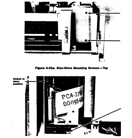
14. Remove the two screws in the bottom of the printer assembly and the screw in the rear right-hand corner of the assembly near the switch-panel tab slot. See figure 6-12. (You may have to move the printhead out of the way to remove one of the screws.)
1 L Lift the printer assembly out of the unit being careful not to damage any of the cables .
•• ",),1.0
-Flgu ... "12. Printer Mountinl Scre.s
8·12 R ... ".I.ncI ... ac .... ent Int ... P.r _ _ Com ...
<