5
VIII
August 2017
Efficiently High Speed Implementation of AES
Algorithm on FPGA
Gurpinder Kaur1, Dr. Amandeep Singh Sappal2 1, 2Department of ECE, Punjabi University, Patiala
Abstract: With the increasing number of internet and wireless communication users in any organisation, data security has become a major problem for the valuable information that needs to be protected. So to protect the user data that is being transmitted over open channels some means of resilient data protection is needed. So AES can be considered as the most widely used modern symmetric key encryption standard for such sensitive data that needs to be kept secured. This paper propounds high speed implementation of AES algorithm while maintain with the minimum amount of hardware resources. The proposed AES algorithm supports 128 bit key length. In order to achieve high speed pipelined architecture is used. The AES-128 design is implemented on FPGA with XC6SLX16-3CSG324 package using Verilog language with the help of Xilinx ISE tool.
Keywords: Advanced Encryption Standard (AES), Field Programmable Gate Array (FPGA).
I. INTRODUCTION
With the increasing need of information data in computer networks and communication technology the need of automated tools for protecting files and other information is growing. This data is handled by public networks and is vulnerable. So for such sensitive data that needs to be kept safe and protected from automated spying or hacking, cryptography becomes important. AES is used as the most widely used symmetric cryptographic algorithm to keep the data confidentiality [1].
In 2001, NIST announced the rijandael algorithm from Belgium has been selected as the Advanced Encryption Standard (AES) algorithm after replacing the Data Encryption Standard (DES) [2]. DES was the block cipher that was the first encryption algorithm recommended by the NIST in 1974 [3].
AES can be implemented both in hardware and software. The software implementation of AES is a slow process and thus consumes lots of processing time and also requires regular updates. Moreover the software implementation results in higher costs. While on the other hand the hardware implementation is fast, reliable and is also suitable for high speed applications, without the need of any system update. Moreover hardware implementation does not require any system resources as used in software implementation of AES. Hardware implementation of AES proves to be physically secured as compared to software implementation as the outside attackers cannot modify them. so due to these reasons hardware implementation is widely used for real time applications. Normally there are two platforms for hardware implementations of AES: (1) Application Specific Integrated Circuits (ASICs) (2) Field Programmable Gate Array (FPGA). Among them FPGA as a platform is more efficient as in FPGA implementation can be updated in order to introduce a new feature partially or during run time. Moreover the currently used FPGAs have several features like block memory (BRAM), Digital Signal Processing (DSP) cores and embedded CPUs [8].
The rest of the paper is organized as follows. Section II presents a brief overview of AES and section III provides the proposed work. Section IV shows the implementation results and finally, section V concludes the paper.
II. ADVANCEDENCRYPTIONSTANDARD
AES is the most widely used symmetric cipher today. AES is a symmetric block cipher that uses the same key for both Encryption and Decryption process. It accepts the input block of size 128 bit only and key size may vary between 128, 192 and 256 bits with iterative rounds of 10, 12 and 14 respectively and thus provides an output of 128 bit cipher text. In this paper the key size of 128 bit is used and each transformation is repeated 10 times.
Internal structure of AES consists of four different transformations which are repeated number of times depending on key length as described in table I.
Table I Key Length And Rounds
Key size(bits) No. of Rounds
192 12
256 14
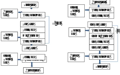
[image:3.612.58.462.176.430.2]Each AES transformation manipulates the 128 bits of data block. When key size of 128 bits is used the transformations are repeated for 10 times. The four transformations of AES Encryption are: SubBytes, ShiftRows, MixColumns and AddRoundKey. In AES Decryption the above transformations are observed in reverse i.e. InvSubBytes, InvShiftRows, InvMixColumns and AddRoundKey [4].
Figure I: Block diagram of AES Encryption and Decryption
A. SubBytes
First transformation of AES is Byte Substitution. It is a non-linear transformation. AES S-Box can be considered as a two step mathematical transformation, where the first step consists of a Galois Field inversion function and the second step consists of affine mapping [9].
1) Inverse SubBytes: Inverse SubBytes is inverse of Byte Substitution layer. It is computed by applying the inverse of affine transformation followed by the multiplicative inverse of GF(2 ).
B. ShiftRows
ShiftRows transformation cyclically shifts the rows of state matrix. The first row of state matrix remains unchanged. The second, third and fourth row is shifted by three, two and one byte to the right respectively. ShiftRows is performed to increase the diffusion properties in the AES.
1) InvShiftRows: in order to reverse the ShiftRows transformation, the shifting is done in opposite direction with respect to Encryption i.e. the second, third and fourth rows of the state matrix are shifted by three, two and one byte to the left respectively. LikeShiftRows, in InvShiftRows the first row of the state matrix remains unchanged.
C. MixColumns: MixColumns is a linear transformation in which each column of the state matrix is mixed independently. In MixColumns transformation each column of 4 bytes is considered as a 4 term polynomial over GF(2 ) and is then multiplied by a polynomial modulo x +1 with a fixed polynomial a(x) given by:
a(x) = {03} + {01} + {01} + {02} MixColumns layer is not present in last round of AES Encryption.
1) InvMixColumns: In order to reverse the MixColumns transformation the inverse of its matrix is used. The columns are considered as polynomials over GF(2 ) and multiplied modulo + 1 with a fixed polynomial (x) given by:
(x) = {0b} + {0d} + {09}x + {0e}
InvMixColumns layer is not present in first round of AES Decryption.
D. Key Addition Layer
Key Addition layer is nothing but xoring operation. Inputs to the Key Addition are current 16 byte state matrix and a 16 byte subkey. State matrix and subkey are combined through bitwise xor operation. Since xor itself is its inverse so the Key Addition Layer remains same for both Encryption and Decryprion.
E. Key Scheduling
The subkeys are derived in the key scheduling. The key schedule takes the original input key(of length 128, 192 or 256 bits) and derives the remaining subkeys. Total number of subkeys derived are number of rounds plus one. AES key schedule is word oriented, where 1 word = 32 bits. for 128 bit key, first it accepts 4 bytes input word and thus performs cyclic permutations. It takes 4 byte words as input and then via byte substitution each byte is substituted by another byte and then xoring is performed using a round constant word array.
Since the AES is a symmetric cipher .i.e. same key is used for both encryption and decryption, so the key computed in last round of encryption is applied to first round of decryption, the second to last computed key is applied to second round of decryption and so on.
III.PROPOSEDWORK
This section describes the modified AES algorithm for high speed with minimum hardware resources.
A. Pipelined Architecture
In this paper pipelined architecture is used for achieving high speed as compared to the previous work [1]. In pipelining when one round is completed simultaneously, the bytes are accepted for the next round. To increase the speed pipelining architecture proves to be very effective. By using the pipelining architecture, the main critical path (i.e. longest propagation path) of the non-pipelined round is being divided into sub-critical paths that will minimize dynamic power that result from unnecessary gate switching by the different signal arrivals in long paths thus leading to lesser delay and finally higher speed. The new sub critical paths in the pipelined architecture can be efficiently optimized in the future at gate and transistor levels [10]. In sub-pipelining, registers are inserted inside the round stages so as to divide the whole round into sub-stages that have approximately equal time delay with multiple blocks of data being processed in the stages and stored in the registers simultaneously.
B. Area and Speed Trade-Off
To achieve maximum operating frequency while maintaining the minimum hardware resources a balances trade-off is to be maintained between the area and speed parameters. So in pipelined architecture the multiple blocks should have equal delay as if there is more load on a single stage than the others then it leads to worst case of pipelining and thus results in increase in hardware. The Encryption round is divided into various stages such that the AddRoundKey is processed in one state round and the SubBytes and ShiftRows are presented in other while the MixColumns transformation is applied in four stages each one for each column so as reduce the complexity of the MixColumns. The use of extra states may lead to the increase in hardware resources so the design must consists of mimimum required states such that the speed of the AES algorithm is increased with the minimum increase in the hardware resources. Unnecessary splitting of states for the sub-pipelined architecture should be avoided to main balanced trade-off between area and speed.
C. Hardware Efficient Architecture
individual register for each round saves hardware and thus leads to lower area consumption. The round key generated in the previous round is kept temporarily stored in the register and is called while AddRoundKey transformation and when the four transformations of the round are completed the next subkey is stored in the register temporarily i.e. the subkey being in use is stored temporarily in the register which provides the key value to the AddRoundKey transformation.
D. AES Data Path Improvement
In AES algorithm control is observed to be independent of data. In this dissertation finite state machine technique (FSM) is used to easily understand the data path during encryption and decryption process. The finite state machine technique is used to represent and control execution flow. This technique provides detailed path to be followed to reach the output.
E. FSM Encryption
Initially when reset is on, no data will be processed and the system is in pre_idle state waiting for the data to encrypt. When reset is set low .i.e. reset = 0, then the system goes to idle state. The system fetches the 16 byte input data block (.i.e. plain text) in idle state. When the data block is ready the system moves to next state (s0). The s0 state indicates the first round of encryption in which the original data .i.e. plain text is xored with original input cipher key. This xored data is applied to S-Box and then after ShiftRow transformation MixColumn is performed. Since the MixColums transformation is a complex process so to reduce the complexity and thus enhance the speed pipelined architecture is used by splitting the MixColumns transformation in four states of FSM, one for each column.So after the first round algorithm moves to second state s1 where the output of first round is xored with the subkey generated using original key and thus applied to the four transformations. Similarly for the next eight rounds this state is repeated in the similar manner. And in the last round all the process remains same except the MixColumn transformation is excluded i.e. the last round of encryption consists of SubBytes, ShiftRows and AddRoundKey. Once the last round .i.e. 10th round is completed the
encryption is done for the first 16 byte data block and thus the Done signal goes high indicating that the encryption is done and the system is ready to encrypt the next 16 byte data block and thus waits for the next data block in the pre_idle state.
F. FSM Decryption
Decryption is the reverse process for encryption. Reset and pre_idle states are similar to those used in FSM Encryption. When reset is low the system moves to idle state and waits for the data to decrypt. When done signal is high it indicates that data is encrypted and is thus ready to decrypt. So system moves to s0 state where first round of decryption is performed which is similar to the last round of encryption i.e. the InvMixColumn layer is absent in first round of Decryption and thus switches to next state which repeats in the same manner for the next eight rounds and includes InvMixColumn transformation and in the last round after completion of last round .i.e. when system decrypts the cipher text back to plain text(input data) it provides a decrypt signal to indicate that decryption is done and the system moves to pre_idle state thus waiting for the new data to arrive.
IV.RESULTSANDCOMPARISONS
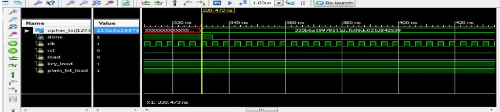
[image:5.612.54.566.599.714.2]For the proposed design of AES algorithm Xilinx ISE 13.2 tool has been used for synthesis and implementation and Xilinx Isim (0.61xd) for testing and verification of simulation results is done on Modelsim tool. The experimental results has been observed using FPGA family XC6SLX16-3CSG324. Simulation results of AES Encryption and decryption are shown in figure II and figure III. The proposed design area utilization for encryption and decryption are summarized in table II and table III along with their performance in comparison to the previous work [1] and the table IV shows the comparison of the area and speed results on various platforms used previously.
Table II Comparison Of Proposed Encryption Design With Existing Work
Parameter Proposed work Existing design [1] AES 128 Regular
Data path(bit) 128 128 128
No. of rounds 10 10 10
Slice Registers 509 564 4800
Slice LUTs 1329 3559 24999
Fully used LUT-FF pairs 403 459 40
Block RAM 1 4 11
Combinational path delay(ns) 0 0 11.992
Max. operating Frequency(Mhz) 285.759 273.997 102.990
[image:6.612.44.562.485.611.2]Figure III: Simulation results for AES Decryption
Table III Comparison Of Proposed Decryption Design With Existing Work
Parameter Proposed work Existing design[1] AES 128 Regular
Data path(bit) 128 128 128
No. of rounds 10 10 10
Slice Registers 580 607 7120
Slice LUTs 2197 3531 39712
Fully used LUT-FF pairs 548 426 3
Block RAM 1 20 10
Combinational path delay(ns) 0 0 8.392
Max. operating Frequency(Mhz) 282.319 223.157 72.489
Table IV Comparison Of Proposed Encryptor With Existing Design
Parameter Proposed Design [5] [6] [7]
Platforms Xilinx Spartan-6
XC6SLX16
Xilinx virtex-5 XC5VL50
Xilinx virtex-2 XC2VP20
Altera APEX20KC
Data path(bits) 128 128 128 128
Area 509 slices/3531
LUT
769 slices/2350 LUT 9028 slices 40960 slices/895 LUT
V. CONCLUSION
AES algorithm plays an important role in the security applications. In this paper, resource efficient high speed AES algorithm is presented in which the speed is increased in such a way that minimum area should increase. A balanced trade-off is maintained between area and speed. The design has the ability to defend against the glitch attacks. The modified design implemented in the dissertation has improvement in hardware efficiency. It shows 10% reduction in slice registers and 59% reduction in LUTs as compared to the existing design [1] encryption and also shows 89.4% reduction in slice registers and 94% reduction in LUTs as compared to the AES 128 regular encryption implementation. Pipelined architecture is used to split the complexity of MixColumns in sub states so as to divide the longest critical path in smaller paths and thus reduces the delay and leads to increase in speed. In terms of speed it shows 4.3% increase in Encryption speed and 26.51% increase in Decryption speed. Thus the implemented algorithm is efficient in terms of area and speed as compared to the existing work [1].
REFERENCES
[1] Pritamkumar N. Khose and Vrushali G. Raut, “Implementation of AES Algorithm on FPGA for Low Area Consumption”, proc. 2015 International Conference on Pervasive Computing (ICPC).
[2] Guang-liang Guo, Quan Qian, Rui Zhang, “Different Implementations of AES Cryptographic Algorithm”, 2015 IEEE 17th International Conference on High Performance Computing and Communications, 2015 IEEE 7th International Symposium on Cyberspace Safety and Security and 2015 IEEE 12th International Conference on Embedded Software and Systems, pp 1848-1853, 2015.
[3] Pournima U. Deshpande and Smita A. Bhosale, “AES Encryption Engines of Many Core Processor Arrays on FPGA by using Parallel, Pipeline and Sequential Technique”, proc. International Conference on Energy Systems and Applications(ICESA), pp 75-80, 30 Oct – 01 Nov 2015.
[4] Christof Paar and Jan Pelzl, “ Understanding Cryptography”, pp 87-117, DOI 10.1007/978-3-642-04101-3 1,_c Springer-Verlag Berlin Heidelberg 2010. [5] Z. Yuan, Y. Wang, J. Li, R. Li and W. Zhao, “FPGA based optimization for masked AES implementation”, Proc. IEEE 54th International Midwest
Symposium on Circuits and Systems (MWSCAS), pp.1-4 2011.
[6] IssamHammad,Kamal El-Sankary, Ezz El-Masry, "High-Speed AES Encryptor with Efficient Merging Techniques" Proc. IEEE Embedded Systems, vol. 2, no. 3, Sept 2010
[7] Hoang Trang, Nguyen Van Loi, “An efficient FPGA implementation of the Advanced Encryption Standard algorithm”, Proc. Computing and Communication Technologies RIVF International Conference, pp. 1-4, 2012.
[8] Rajpreet Singh, Tripatjot Singh Panag, Amandeep Singh Sappal, “FPGA implementation of Optimized Decimation Filter for Wireless Communication Receivers”, International Journal of Innovative Research in Computer and Communication Engineering, vol. 2, issue 4, April 2014.
[9] FIPS 197, Advanced Encryption Standard http://csrc.nist.gov/publications/fips/fips197/fips-197.pdf
![Table II Comparison Of Proposed Encryption Design With Existing Work Proposed work Existing design [1]](https://thumb-us.123doks.com/thumbv2/123dok_us/8307336.856645/6.612.49.559.84.453/table-comparison-proposed-encryption-design-existing-proposed-existing.webp)
