University of New Orleans University of New Orleans
ScholarWorks@UNO
ScholarWorks@UNO
University of New Orleans Theses and
Dissertations Dissertations and Theses
8-9-2006
Hardware/Software Co-Design Architecture and Implementations
Hardware/Software Co-Design Architecture and Implementations
of MIMO Decoders on FPGA
of MIMO Decoders on FPGA
Cao Liang
University of New Orleans
Follow this and additional works at: https://scholarworks.uno.edu/td
Recommended Citation Recommended Citation
Liang, Cao, "Hardware/Software Co-Design Architecture and Implementations of MIMO Decoders on FPGA" (2006). University of New Orleans Theses and Dissertations. 416.
https://scholarworks.uno.edu/td/416
HARDWARE/SOFTWARE CO-DESIGN ARCHITECTURE AND
IMPLEMENTATIONS OF MIMO DECODERS ON FPGA
A Thesis
Submitted to the Graduate Faculty of the University of New Orleans in partial fulfillment of the requirements for the degree of
Master of Science in
The Department of Electrical Engineering
by
Cao Liang
B.S., UESTC, 2002
August 2006
ACKNOWLEDGEMENT
Many people from different parts of my life have contributed to my success in completing
this thesis. First and foremost I would like to express my deepest gratitude to my committee
members Dr. Xinming Huang, Dr. Jing Ma and Dr. Vesselin Jilkov for the continuous support
and shared knowledge. I would like to offer a special thanks to Dr. Jing Ma and Dr. Xinming
Huang for providing me the opportunity to work on this project and for their invaluable
inspiration and suggestions which make it possible for me to finish this thesis. I am very grateful
to Dr. Xinming Huang for serving as my committee chair and guiding me to the right direction
during the long graduation process. I would also thank Dr. Vesselin Jilkov for his insightful ideas
and comments to the thesis.
Last, I take this opportunity to thank my parents and wife for their unconditional support and
TABLE OF CONTENTS
List of Figures ...v
List of Tables ... vi
Glossary of Abbreviations ... vii
Abstract ... ix
Chapter 1 Introduction ...1
1.1 Motivations and background ...1
1.2 Research objectives ...5
1.3 Contributions ...5
1.4 Organization of the thesis ...6
Chapter 2 MIMO system and sphere decoding algorithms ...7
2.1 Introduction to MIMO system ...7
2.1.1 Antenna diversity gain ...8
2.1.2 Spatial multiplexing gain ...8
2.2 Lattice decoding problem ...9
2.3 Sphere lattice decoding algorithms ...10
2.3.1 VB decoding algorithm ...11
2.3.2 AV decoding algorithm ...16
Chapter 3 Hardware/software co-design and developing board ...21
3.1 Introduction to hardware/software co-design ...21
3.2 FPGA structure ...23
3.3 Design flow and developing board ...25
Chapter 4 Hardware/software architecture for MIMO sphere decoders ...29
4.1 Partitioning of the sphere decoding algorithms ...29
4.2 Processor level parallelism ...31
4.3 Complex constellation parallelism ...32
4.3.1 Conventional 2M-dimensional search method ...33
4.3.2 Two M-dimensional search method ...34
4.3.3 Simulation validation ...37
4.4 State level parallelism ...38
4.4.1 Data flow dependency analysis ...39
4.4.2 Hardware architecture of state level parallelism ...40
5.1 MicroBlaze soft core prototype performance ...43
5.2 Hardware synthesis performance ...44
5.3 Decoding rate performance ...46
5.4 BER performance ...50
Chapter 6 Conclusions ...53
References ...54
List of Figures
Figure 2.1 Block diagram of MIMO system ...7
Figure 2.2 State representation of VB algorithm ...13
Figure 2.3 Flowchart of modified VB algorithm ...15
Figure 2.4 State representation of AV algorithm ...18
Figure 2.5 Flowchart of AV algorithm ...19
Figure 3.1 Xilinx FPGA-based hardware/software co-design architecture ...22
Figure 3.2 Xilinx FPGA structure ...25
Figure 3.3 Design flow for FPGA-based HW/SW co-design systems ...26
Figure 3.4 Xilinx EDK workspace ...27
Figure 3.5 XUP Virtex-II Pro developing board ...28
Figure 4.1 Architecture of the processor level parallelism ...31
Figure 4.2 Number of states visited vs. number of antennas ...34
Figure 4.3 Architecture of complex constellation parallelism ...36
Figure 4.4 Comparisons of BER performances of two transformation methods ...37
Figure 4.5 Comparisons of number of states visited of two transformation methods ...38
Figure 4.6 Data flow dependency graph of AV algorithm ...39
Figure 4.7 Data flow dependency graph of VB algorithm ...40
Figure 4.8 Architecture of state level parallelism for AV decoder ...41
Figure 4.9 An example of state level parallelism for AV decoder ...42
Figure 5.1 Number of states visited for different initial radiuses in VB decoder ...47
Figure 5.2 Comparisons of decoding rates for different sphere decoders ...50
Figure 5.3 BER performances for VB sphere decoders ...51
List of Tables
Table 3.1 Xilinx XC2VP30 FPGA features ...25
Table 5.1 MicroBlaze soft core timing performance ...44
Table 5.2 Resource utilization of real or imaginary part decoder ...45
Table 5.3 FPGA resource utilization for AV and VB sphere decoders ...45
Table 5.4 Average state visit statistics for AV and VB decoders at 20 dB Eb/N0 ...48
Glossary of Abbreviations
ALU – Arithmetic Logic Unit
ASIC – Application Specific Integrated Circuit
AWGN – Additive White Gaussian Noise
BER – Bit Error Rate
BRAM – Block Random Access Memory
CAD – Computer Aided Design
DSP – Digital Signal Processor
Eb/N0 – Bit Noise Ratio
EDK – Embedded Development Kit
FPGA – Field Programmable Gate Array
FSL – Fast Simplex Link
FSM – Finite State Machine
HW/SW – Hardware/Software
IC – Integrated Circuits
I/O – Input Output
IOB – Input Output Bus
ISE – Integrated Software Environment
MB – MicroBlaze
MIMO – Multiple Input Multiple Output
ML – Maximum Likelihood
NRE – non-recurring engineering
OPB – On-chip Peripheral Bus
PAR – Place and Route
PLB – Processor Local Bus
PLD – Programmable Logic Device
QAM – Quadrature Amplitude Modulation
QoS – Quality of Service
RISC – Reduced Instruction Set Computer
RTL – Register Transfer Level
SISO – Single Input Single Output
SoC – System on a Chip
SoS – System on Silicon
SNR – Signal Noise Ratio
VHDL – Very high speed integrated circuits Hardware Description Language
VLSI – Very Large Scale Integration
Abstract
During the last years, multiple-input multiple-output (MIMO) technology has attracted great
attentions in the area of wireless communications. The hardware implementation of MIMO
decoders becomes a challenging task as the complexity of the MIMO system increases. This
thesis presents hardware/software co-design architecture and implementations of two typical
lattice decoding algorithms, including Agrell and Vardy (AV) algorithm and Viterbo and
Boutros (VB) algorithm. Three levels of parallelisms are analyzed for an efficient
implementation with the preprocessing part on embedded MicroBlaze soft processor and the
decoding part on customized hardware. The decoders for a 4 by 4 MIMO system with 16-QAM
modulation scheme are prototyped on a Xilinx XC2VP30 FPGA device. The hardware
implementations of the AV and VB decoders show that they support up to 81 Mbps and 37 Mbps
data rate respectively. The performances in terms of resource utilizations and BER are also
Chapter 1
Introduction
1.1
Motivations and background
Because of the scarce spectrum bandwidth provided for modern wireless systems, the
traditional single-input single-output (SISO) channel can not meet the continuously increasing
demands for channel capacity and quality of service (QoS) in wireless communications. By
introducing multiple antennas into both transmitter and receiver, MIMO technique has emerged
as a key technology for the next generation wireless systems.
MIMO communication system can significantly increase the channel throughput and provide
better link reliability [1][2][3] at the same bandwidth and same overall transmit power of the
SISO communication system. In MIMO system, multiple data streams are transmitted through
different antennas at the same time using the same frequency, which is so called spatial
multiplexing. Because of this multipath propagation, each output of the receive antenna is a
linear combination of all transmitted streams. Then the extremely high throughput is achieved by
separating data streams on the receiver using proper decoding algorithms. In addition, QoS is
improved because of spatial diversity advantage, since each receive antenna has a measurement
of all transmitted data streams. In general, the spectrum efficiency and the propagation range
have been greatly increased due to the spatial multiplexing gain and the diversity gain provided
by MIMO technique. Combined with orthogonal frequency division multiplexing (OFDM),
All of these promising performance improvements resulting from MIMO system are
achieved at a cost of increased computational complexity especially in the decoders at the
receiver side. In a multiple-antenna channel environment, each transmitted signal is aligned on
the modulation constellation points. By multiplying all possible signal sets with the MIMO
channel matrix, it generates a set of finite points in a multiple-layered lattice structure. The
MIMO decoding problem is essentially to search for the closest lattice point to the received point.
The optimal detection strategy for a MIMO decoder is to perform a maximum likelihood (ML)
search over all possible points inside a lattice structure and find the best one with smallest
Euclidian distance to the received signal. But in reality, this method is not practicable because
the corresponding computational complexity grows exponentially with the number of transmit
antennas M and the number of bits Q used to represent a symbol, since the detector needs to
examine all 2MQ possible lattice points for each received vector. For example, in a MIMO system
with 4 transmit and 4 receive antennas using 16-QAM modulation scheme, a total of 65536
candidates have to be examined to find the optimal vector. This method is also referred as
exhaustive search. An efficient hardware implementation of the decoders has become a key
challenging task in MIMO wireless system design.
There are two typical strategies of MIMO detection algorithms used to accelerate the
decoding procedure in an arbitrary lattice structure given by its generation matrix. One is the
Pohst strategy proposed in 1981 [5], which examines lattice points lying inside a hyper sphere.
The decoding algorithm developed by Viterbo and Boutros [6] is based on this strategy and is so
Schnorr and Euchner in 1994 [7], which performs the point search inside the aforementioned
hyper sphere with a zig-zag order in each lattice layer with increasing distances from the
received vector. A representative lattice decoding algorithm based on this strategy is introduced
by Agrell, Eriksson, Vardy and Zeger [8] and is called the AV algorithm. Both algorithms solve
the ML detection problem and are commonly referred as sphere decoding algorithms because
they search for the closest lattice point in a hyper sphere. Both algorithms are considered as the
most promising solutions for the MIMO decoders. A detailed analysis and efficient architecture
for both algorithms will be discussed in Chapter 2 and Chapter 4 respectively.
Due to the complexity and high data dependency involved in the decoding algorithms, the
MIMO decoders are traditionally implemented on digital signal processors (DSPs), such as Bell
Labs layered space-time (BLAST) system [9][10]. Because of not supporting parallelism, a
single DSP based implementations can hardly achieve very high decoding rate for MIMO system,
especially as the number of antennas increases. Very large scale integrated circuit (VLSI)
architecture of MIMO systems has also been studied recently. It is a challenging task to achieve
the real-time performance of the sphere decoder due to the complexity of VLSI implementation.
Several hardware implementations have been reported by prototyping the VLSI architecture of
the VB algorithm, AV algorithm or their extended versions [11][12]. Most recently, Burg,
Bormann, and etc have declared a high processing rate for MIMO decoders on an application
specific integrated circuit (ASIC) implementation [13]. But the ASIC implementation is
Field programmable gate array (FPGA) devises are also widely used in signal processing
field due to their flexible reconfiguration and support of parallelism. Combined with their huge
processing capabilities, high data rates are ensured for many computational intense algorithms
implemented in FPGAs.
The main advantage provided by FPGAs when compared with DSP implementation is the
huge performance gains brought by the opportunity to execute the computationally intensive
procedures in parallel of an algorithm. Although the design cycle is longer than DSP
implementation, once an efficient architecture is developed and the possible parallelisms are
explored, FPGA is able to significantly improve the computation throughput. Another advantage
of FPGA is the customizability since the processing capacity is scalable based on the FPGA
resources and the applications have the flexibility to be upgraded even during the run-time to
keep up with changing standards.
Compared with ASIC applications, the implementing of design changes is much easier and
the time-to-market cycle is much shorter in FPGA implementations. Furthermore, for system
prototyping the overall cost of an FPGA design is much lower than that of an ASIC design.
In addition, the hardware/software (HW/SW) co-design concept has been adopted by FPGA
lately by introducing one or more embedded processors into FPGA design, e.g. the PowPC (PPC)
or MicroBlazeTM (MB) on Xilinx FPGAs [14][15] and Nios processors on Altera FPGAs [16].
HW/SW co-design technique generally partitions the computational algorithm into customized
hardware to achieve high computational speed and into embedded soft processors to reduce the
to execute the processing tasks that are less time critical but highly sequential or considerably
complicated for direct circuit implementation. This thesis will explore the FPGA-based HW/SW
co-design architecture for both AV and VB lattice decoding algorithms.
1.2
Research Objectives
The main objective of this thesis is to develop efficient HW/SW co-design architecture of
sphere decoders for both AV and VB algorithms and prototype it on Xilinx University Program
(XUP) Virtex-II Pro developing board [17]. The decoding rates are also examined based on the
hardware implementations.
1.3
Contributions
The hardware implementation of MIMO decoders with high decoding rate is a challenging
and urgent task in multiple-antenna wireless communications. The main contributions of this
thesis are summarized as follow:
The FPGA-based HW/SW co-design architecture for MIMO decoders with complex
constellation structure is proposed, which partitions the complicated channel matrix
preprocessing including matrix inversion and factorization into soft processor and the iterative
decoding procedures into customized hardware modules. This architecture is able to significantly
improve the decoding rate, and meanwhile keeps it easy to be implemented in hardware.
Three levels of parallelisms are also explored to accelerate the decoding processing: the
concurrent execution of the preprocessing on embedded processor and decoding functions on
Both AV and VB decoders are simulated in ModelSim [18], developed in EDK [19] and
implemented on XUP Virtex-II Pro developing board with an XC2VP30 FPGA. The hardware
results are also verified by the MATLAB software simulations.
System performances including BER, data rate, and resource utilizations are compared
between these two decoding algorithms. To the author’s knowledge, the real-time performance of
the system prototypes are among the fastest MIMO decoders reported thus far.
1.4
Organization of the thesis
The rest of the thesis is organized as follow. Chapter 2 reviews the principles of MIMO
system and two sphere lattice decoding algorithms. The step by step decoding procedure and
state based flow charts are given and analyzed for both AV and VB algorithms. Chapter 3 gives
the introduction to FPGA structure and hardware/software co-design procedures. Three levels of
parallel structures for the complex sphere decoders are explored in Chapter 4. The complex
constellation parallelism is derived theoretically and verified by MATLAB simulations. The data
flow dependency among the iterative searching procedure is also analyzed to achieve the state
level parallelism in this chapter. Comparisons of the experimental results between these two
Chapter 2
MIMO system and sphere decoding algorithms
This chapter gives a brief introduction to MIMO system. Two typical sphere decoding
algorithms are described in details and are further analyzed for hardware architecture design.
2.1
Introduction to MIMO system
During recent years, MIMO technology has emerged as a promising solution for the ever
increasing demands of higher data rate and better QoS in wireless communications. By applying
multiple antennas at both transmitter and receiver sides, MIMO system is able to greatly enhance
the spectral efficiency and also provides a better range of coverage than the traditional SISO
system. Recent initiatives for standardization of future MIMO systems including UMTS (3GGP
Release 7), IEEE 802.11n wireless LAN, and IEEE 802.16 WiMax reflect the importance of
MIMO technique.
Figure 2.1 Block diagram of MIMO system
Modulatio
n
Demux
S1
S2
SM
u1
u2
uM
M antennas
Decoder
y1
y2
N antennas
yN
1
ˆ
u
2
ˆ
u
Demodulation
MIMO channel
Mux
M
u
ˆ
Sˆ
S
Figure 2.1 gives a schematic representation of a MIMO system. The original signal S is
split into M lower rate data streams, modulated and transmitted simultaneously from each
transmit antenna. The receiver, having complete knowledge of the channel, decodes these
individual data streams, demodulates them and combines them together so as to recover the
original signal. In the wireless MIMO channel, each data stream is transmitted through different
data paths to reach different receive antennas. Two performance gains are provided by this
multipath propagation method.
2.1.1 Antenna diversity gain
Fading is generally a cumbersome problem in wireless communications. When the signal
power drops significantly, the channel is said to be in a fade, which gives rise to BER and
reduces the signal coverage range. In MIMO system, replicas of the same transmitted signal are
provided across different antennas at the receiver side through independent fading paths. When
one path is in fade, it is unlikely that all other paths are also in deep fade. Hence the more
reliable reception is achieved in MIMO system. This QoS gain brought by MIMO system is
called antenna diversity gain or spatial diversity gain.
2.1.2 Spatial multiplexing gain
The spatial multiplexing is to transmit the split data streams concurrently through different
transmit antennas, which helps to increase the data transmission rate for the same bandwidth and
with no additional power expenditure. This performance gain is only possible in MIMO system.
The capacity of the wireless channel grows linearly with the number of transmit antennas. Thus
technique uniquely important in modern wireless communications with scarce spectrum
bandwidth.
2.2
Lattice decoding problem
Design an efficient decoder for MIMO receiver to match with the high transmission rate has
become a challenging task, because the high computational complexity is involved especially in
high dimensional MIMO systems with complex signal constellation.
Considering a MIMO system with M transmit N receive antennas, the received vector y is
given by:
n H u
y = + Eq 2.1
where u is the 1×M transmitted signal vector, and n is a 1×N additive white Gaussian
noise (AWGN) vector with zero mean and variance. H is the M×N channel transfer matrix
which is assumed to be known by the receiver. Each element in the H matrix corresponds to one
fading coefficient between one transmit-receive antenna pair. For selected modulation scheme,
each element in
0
N
u is represented by one of the constellation points. A lattice structure, denoted
as Λ, is generated by multiplying all possible u with H. The ML lattice decoding problem is
to find the closest lattice point to the received point in the lattice structure:
uˆ argmin|| y uH ||2
u −
=
Λ
∈ Eq 2.2
where uˆ is the decoded vector. Thus the ML-based decoding system can be summarized as:
Input: The channel lattice generation matrix H and the received vector y.
2.3
Sphere lattice decoding algorithms
The optimal lattice decoding method is to examine all possible lattice points in the lattice
structure and find the best one with minimum Euclidian distance to the received vector. However,
this method is not a solution for practical MIMO decoders because of the extreme complexity
involved in this exhaustive search.
Two sphere decoding algorithms are analyzed in this section, named AV and VB algorithms.
Both algorithms are ML-based lattice decoding algorithms, which try to enumerate the lattice
points inside a sphere, and find the closest one to the received vector. The main difference
between these two algorithms is the investigating order inside the lattice structure. The VB
algorithm searches from the lower bound to the upper bound in each search layer and examines
all possible lattice points falling into a certain sphere in the lattice structure with an initial radius
C. Meanwhile the AV algorithm spread out from a nearby lattice point to the received point and
terminates once the total distance is greater than the best distance and the search procedure
reaches the bottom layer. No initial radius is needed in the AV algorithm, and it does not need to
upgrade the lower and upper bounds of each layer using the time consuming square root
functions as it needs in the VB algorithm. It is claimed that the AV algorithm is about 2 to 8
times more efficient than the VB algorithm [8] even if a proper initial radius C is applied to
the VB algorithm.
The step by step procedure for each algorithm is presented below. To improve the efficiency
of the VB algorithm, a modified version of VB algorithm is adopted in this thesis, which avoids
2.3.1 VB decoding algorithm
Two lattices are identical if all the lattice points generated by the lattice matrices and given
signal set are the same. So basis reduction can be performed on the lattice generation matrix H to
reduce the complexity of the decoding procedure. In the VB algorithm, Cholesky factorization is
applied to the gram matrix , and it yields , where R is an upper triangular
matrix. Thus the squared Euclidian distance shown in Eq 2.2 can be rewritten as:
T
HH
G= G=RTR
2 2 2 2 2 || ) ( || || ) ( || ) ( ) ( ) ( ) ( || ) ( || || || T T T T T T u R R u u R R u u HH u H u H u y d − = − = − − = − − = − = − = ρ ρ ρ ρ ρ ρ ρ Eq 2.3
where ρ =yH−1. By properly chosen the C, the searching range becomes a sphere with
square radius C centered at the received point. And thanks for the attributes of the upper
triangular matrix, the squared distance can be constrained by the following inequation:
d u r u r u C
M i M i j j j ij i i
ii − + − ≤
=
∑
∑
= =+ 2 1 1 2 ) )) ( ( ) ( ( ) ,(ρ ρ ρ Eq 2.4
Substituting ξi =ρi −ui, qii =rii2 for i = 1,…,M and qij =rij/rii for i = 1,…,M, j = i+1,…,M
into Eq 2.4:
d u q q C
M i M i j j ij i
ii + ≤
=
∑
∑
= =+ 2 1 1 2 ) ) ( ( ) ,(ρ ξ ξ Eq 2.5
Starting from the bottom row of matrix R and working backwards, the upper and lower
C q q M i j j ij i
ii +
∑
≤+ = 2 1 ) ) (
(ξ ξ Eq 2.6
where ui is used to represent the examining index of layer i and Li denotes the upper bound of ui.
So the initial ui, which is essentially the lower bound of the examining index, and Li for each
layer is determined by:
⎣
⎦
⎡
/⎤
1/ − + − = + = i ii i i i ii i i S q T u S q T L Eq 2.7
where
⎣ ⎦
x is the smallest integer greater than x, and⎡ ⎤
x is the greatest integer smaller than x.And:
∑
Eq 2.8 + = + = M i j j ij i i q S 1 ξ ρ 2 1 i ii( i i)i T q S u
T− = − − Eq 2.9
The VB-based decoder searches from the bottom layer to the top layer and scans each lattice
index from the lower bound to the upper bound. When the algorithm reaches the top layer
without violating the bound constraint, a valid lattice point is found. Then the new distance dnew
between the valid lattice point and the received point is calculated and compared with the
currently best distance dbest, which is initialized to be equal to C. If dnew is smaller than dbest, a
closer lattice point is found and stored as the currently best lattice point. The searching radius is
upgraded to dnew. This process iterates until all the lattice points within the sphere are examined.
The flow chart and more details of this VB algorithm are available in [6]. In this thesis, the VB
Step 1: Preprocessing and initialization:
Transform H into an upper triangular matrix by Cholesky [20] factorization algorithm. Calculate
1
− = yH
ρ . Initialize the sphere radius C by an
adaptive method [21]. Set dimension index i=M and dbest= C. Find the upper bound LM and index
uM .
Step 2: Finite State Machine (FSM) Upgrade ui= ui +1.
If ui < Li and i>1 go to State A;
If ui < Li and i=1 go to State B;
If ui > Li go to State C.
Step 3: State A:
Expand the layer into (i-1)-dimensional sublayer and find the Si and Ti used to upgrade ui and Li.
Goes to State D.
Step 4: State B Upgrade dnew.
If dnew < dbest, record the currently best distance
and the best point. Set i=M. Go to State D. If dnew > dbest, go to step2.
Step 5: State C
Stop if i=M, otherwise move the procedure one step up i=i+1, and go to step 2;
Step 6: State D
Upgrade ui and Li, and go to step 2.
Figure 2.2 State representation of VB algorithm
As shown in Figure 2.2, basis reduction is performed to reduce the complexity of decoding
procedure before the closest point search begins. This is called preprocessing, which involves
Cholesky decomposition and matrix inversion. These complex matrix manipulations are difficult
and too costly for hardware implementation, and they are not executed frequently in the sphere
decoding algorithm. So only the iterative decoding procedures are considered to be implemented
clear that State D carries much more computational load than other states. This is because the
hardware inefficient square root functions are used to upgrade ui and Li. The requirements of the
square root functions make the computation load unbalanced among the four states. Furthermore,
State D counts for about 40% of the total number of states visited for a vector to be decoded in
MATLAB simulation. Thus the State D becomes the dominant computational part in the VB
algorithm, which can not take full parallelism advantage of FPGAs. To design an efficient FPGA
architecture, the VB algorithm must be modified to avoid the square root calculations. One of the
modified versions of the VB algorithm is presented in [22], which suitably matches the
FPGA-based design.
The purpose of the square root computations in the original VB algorithm is to find the lower
and upper bounds for the examining index in each layer. Because the points in a lattice structure
are generated from the transmitted signal vectors, the examining index ui should also come from
the signal constellation points. Besides, in coherent demodulations the modulation scheme is
known by the receiver. Thus a new method to determine the searching range for the examining
index can be achieved by directly substituting each symbol of the signal constellation into Eq 2.6.
Redefine Ti as:
Ti =qii(Si −ui)2 Eq 2.10
where Si remains the same as in Eq 2.8. The partial distance at the ith layer can be rewritten as:
P q S x T C k K Eq 2.11
M
i j
j k
i ii
k ( ) , 1,...,
1
2 + ≤ =
−
=
∑
+ =
and ui can be upgraded as: K k C P P where x u C P and x L k t t i k k i ,..., 1 , ) min( , 1 ), max( = ≤ = − = ≤ = Eq 2.12
The flow chart of the modified VB algorithm is given below:
M l T and S C d H y G Cholesky q HH G l l l best j i T ,..., 1 , 0 , ; ); ( ) ( , 2 1 , = = = = = = = − ρ ρ
Figure 2.3 Flowchart of modified VB algorithm
The changes of the modified VB algorithm are subtle but significant. Instead of calculating Y N Y M i= C P and x L K k C P P where x u C T x s q P k k i k t t i M i j j k i ii k ≤ = = ≤ = − = ≤ + − =
∑
+ = ) max( ,..., 1 , ) min( , 1 ) ( 1 2 2 ) ( 1 i i ii i i i u S q T u u − = + = N∑
= = M i i new T d 1 2 Y State B 1 , 1 1 1 − = + = − =∑
= − − − i i q S u M i j j j i i i i i i ξ ρ ρ ξ 1 + =i iui >Li
State C
N
i =M
Y
Output ubest
i >1
the examining range by the constraint radius C, the symbols from the signal constellation are
directly used to calculate all possible partial distances in the ith layer. And the examining index ui
is restricted to the qualified symbols. There are at least three advantages brought by this method:
Firstly, it avoids the square root functions, and the partial distances Pk can be calculated in
parallel to achieve an efficient hardware implementation. Secondly, within the signal
constellation, the number of the examining points is more likely to be reduced compared with the
original method, which makes the received vector to be decoded faster than the original VB
algorithm. At last, it guarantees that all the examining points are coming from the signal
constellation points which leads to a better BER performance.
Although an efficient searching procedure can be conducted by the improved VB algorithm,
the choice of the initial sphere radius C is very crucial to the decoding speed. If the radius is
too small, the search will fail and no lattice point within the sphere will be found. However large
C means more points will be examined during the searching procedure and longer time will be
spent for one vector to be decoded. Thus the decoding rate will be greatly degraded if the radius
is too large. An adaptive method to calculate the radius C is discussed in Chapter 5.
2.3.2 AV decoding algorithm
Instead of examining the lattice points from the lower bound to the upper bound in each layer,
the AV algorithm starts from the Babai point [23], and spreads out within the distance between
the Babai point and the received point.
The lattice generation matrix H is decomposed into an M×M lower triangular matrix R and
whereH =R−1Q. Then Eq 2.1 can be rewritten as: T T Q n R u Q y n Q R u y + = + = − − 1 1 Eq 2.13
The AV decoding problem is formulated as:
ˆ argmin|| −1||2 Λ
∈ −
= yQ uR
u T
u Eq 2.14
The index ui is calculated and examined in the order shown in Eq 2.15 and Eq 2.16:
ei = yQTR Eq 2.15
ui ={[eii],[eii]±1,[eii]±2,...} Eq 2.16
where [x] finds the closest integer to x. The orthogonal distance in the ith layer is given by:
d =(eii −ui)/rii Eq 2.17
where rii is the ith diagonal element in R. The partial distance dnew in the ith layer is upgraded by
Eq 2.18 if it is smaller than the currently best distance dbest:
∑
Eq 2.18= = = − = M i j M i j jj j jj
new e u r d
d2 (( )/ )2
∑
2And the closest point search expands to the (i-1) dimensional sublayer by:
ei−1,j =eij −drij, j=1,...,i−1 Eq 2.19
On the other hand, if the partial distance is greater than dbest, the search procedure steps 1 layer
back, and the examining index in this layer is upgraded in the order shown in Eq 2.16. This
zig-zag order leads to a nondecreasing distance to the received vector y in each layer. The
searching procedure terminates when it moves down to the bottom layer without finding a closer
Step 1: Preprocessing and initialization: Transform H into a lower triangular matrix by QR [25] decomposition algorithm. Initialize dimension index i=M. Find the bounded index uM and the
orthogonal distance d from y to the
layer with index uM.Set dbest=∞.
Step 2: Finite State Machine (FSM) Upgrade dnew using d.
If dnew < dbest and i>1 go to State A;
If dnew < dbest and i=1 go to State B;
If dnew > dbest go to State C.
Step 3: State A:
Expand the layer into (i-1)-dimensional sublayer and find d and bounded ui. Go
to step 2.
Step 4: State B
Record the currently best distance and the lattice point. Set i=2, and find d and bounded ui. Go to step 2.
Step 5: State C
Stop if i=M, otherwise move the procedure one step up i=i+1, and find d and bounded ui. Go to step 2;
Figure. 2.4 State representation of AV algorithm
Similar to the VB algorithm, the matrix preprocessing involves QR decomposition and
matrix inversion, which is only needed to be upgraded once in a signal frame length (typically 10
ms). Thus only the iterative decoding functions are considered to be implemented on FPGA. By
analyzing the three states involved in the AV algorithm, it is clear that the computational load is
well balanced among these states, and no complicated calculations are introduced into the
decoding procedure. Furthermore, based on the data flow dependency among these states, the
architecture.
The flow chart of the AV algorithm is also given in Figure 2.5:
Preprocessing: Calculate R,QT
Find eM,uMand orthogonal distance
Initialization: Set i=M and dbest=∞
Upgrade dnew
dnew< dbest?
Figure 2.5 Flowchart of AV algorithm
Compared with the VB algorithm, the advantages of using the investigating order in Eq 2.16
are obvious. Firstly, it does not need to calculate and upgrade the upper and lower bounds in each
layer which involves intensive computations in the VB algorithm. Secondly, by using this
nondecreasing distance order to search inside each lattice layer, the chance of finding the correct i=1?
State A:
Expand to i-1 dimensional sublayer: i=i-1. Find ui and d
State B:
Record currently best lattice point
i= 2. Find ui and d
State C:
If i=M, stop; Else move one layer up: i=i+1. Find ui and d
N Y
point, no initial radius C is needed in the AV algorithm. Literature results show that the
AV-based decoder is about 2 to 8 times faster than the VB-based decoder [8]. Efficient
hardware/software co-design architecture is designed for both algorithms in Chapter 4, where the
Chapter 3
Hardware/software co-design and developing board
3.1
Introduction to hardware/software co-design
The term of hardware/software co-design surfaced in the early 90s when rapid reduction in
the size of integrated circuits (ICs) made it possible to have embedded processor(s) on the same
hardware silicon or chip, which is so called System on Silicon (SoS) or System on a Chip (SoC).
It has moved from an emerging discipline to a mainstream technology [26], and is applied in a
vast number of areas. The principle of HW/SW co-design technique is to partition the
applications into the embedded processors and the customized hardware modules. The goal of
this architecture is to enhance the system performance while reducing the design effort and costs,
which is achieved by the benefits from HW/SW co-designs. The advantages of using processors
lie in the following aspects: First, software is more flexible and cheaper than hardware, which
allows late design changes and simplified debugging opportunities [35]. Furthermore, the
available software libraries make many computationally complicated functions easy to be
implemented inside the microprocessors. Finally, the possibility of reusing software by porting it
to other processors, reduces the time-to-market cycle and the design effort. On the other hand,
the hardware is always used to implement the computationally intensive tasks, which can
extraordinarily improve system performance by the parallel executions. With a flexible and high
speed interface between the hardware and software cores, this architecture can greatly speed up
ASICs and FPGAs are both widely used in the HW/SW co-design systems. ASICs provide a
dedicated hardware solution, which can usually lead to the best hardware performance at the
expense of long design cycle and high non-recurring engineering (NRE) charges. On the other
hand, FPGAs provide more flexibility and shorter design time than ASICs at a higher cost per
unit device. It is a perfect platform for system prototyping and low-volume products. During past
a few years, traditional FPGAs have combined with embedded microprocessors and related
peripherals to form complete SoCs. Examples of this hybrid technology can be found in Xilinx
Virtex-II Pro, Virtex-4 devices and Altera Stratix FPGAs. In this thesis, Xilinx Virtex-II Pro
developing board is chosen to be the test bench for the MIMO decoders. The Xilinx FPGA-based
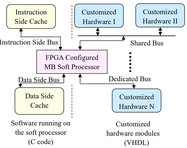
HW/SW co-design architecture is given below:
Customized hardware modules
(VHDL) FPGA Configured
MB Soft Processor
Data Side Cache Instruction Side Cache
Software running on the soft processor
(C code) Instruction Side Bus
Data Side Bus
Shared Bus
Dedicated Bus Customized
Hardware I
Customized Hardware II
Customized Hardware N
The Xilinx MicroBlaze soft core, which is licensed as part of Xilinx EDK, is a 3-stage
pipeline 32-bit RISC processor with 32 general purpose registers, ALU and a rich instruction set
optimized for embedded applications. It is implemented by general logic primitives within the
FPGA logics [15]. The MicroBlaze solution is designed to be flexible, giving the user control of
a number of features such as the cache size, interfaces, and execution units. The configurability
allows the user to trade-off features for size, in order to achieve the necessary performance for
the target application at the lowest possible cost. Multiple customized hardware modules can be
attached to the MB for hardware functions through interfaces such as on-chip peripheral bus
(OPB), fast simplex link (FSL) or processor local bus (PLB). The software functions are
executed inside the MB soft core with the instructions and data provided by instruction side
cache and data side cache. C code and VHDL code are used to describe the software and
hardware designs respectively. By properly partitioning of an application, the HW/SW co-design
architecture is able to greatly enhance the computational performance of the whole system
meanwhile keeps the flexibility of complicated manipulations inside the MB executions.
3.2
FPGA structure
There are three typical types of ICs, programmable logic devices (PLDs), ASICs and FPGAs.
With predetermined architecture by manufacturer, PLDs can provide great programmable
flexibility for engineers to perform a variety of different functions. But these devices contain a
relatively limited number of logic gates which is only suitable for some simple and small
implementations. But the designing of ASIC systems is too time consuming and costly. And once
the final design is finished, it can not be modified to adapt to any application changes.
FPGAs stand in the middle of PLDs and ASICs, which contain programmable logic blocks along
with configurable interconnections between them [27]. Their functionality can be reconfigured in
the way like PLDs, and they can contain millions of logic gates to provide a performance lean
more toward to that of ASICs. The cost of an FPGA design is much lower than that of an ASIC.
Meanwhile the design changes, even at the run-time, are implemented much easier in FPGAs.
Thus, FPGA is considered as an ideal platform to perform the computationally intensive
operations involved in the sphere decoding algorithms for reasons of performance, cost and
reconfigurability. Xilinx and Altera are the two major manufacturers in FPGA market. Each
company has a variety of FPGA series, which suit for different design requirements. Figure 3.2
shows the structure of Xilinx FPGAs. The Xilinx FPGA device is organized as an array of logic
elements, named slices, and programmable routing resources used to provide connections
between the slices, FPGA I/O pins, on-chip block memory and other resources [28]. Each slice
contains two logic cells, which can be performed as a 16-bit register or conducts the functions of
basic logic gates such as AND, OR, XOR, and etc. By properly combining these basic logic
elements, certain circuits can be generated to perform more complex combinatorial functions.
Multipliers are inherently slow if implemented by connecting a large number of programmable
logic blocks together. Xilinx FPGAs incorporate special hardwired embedded multipliers to
Figure 3.2 Xilinx FPGA structure [28]
The Xilinx Virtex-II Pro XC2VP30 FPGA is chosen as the test bench device for this thesis
research. The available resources of particular interest to our design are listed in Table 3.1
FPGA XC2VP30
Number of slices 13969
Number of External IOBs 896
Number of embedded 18×18 MULT 136
Size of BRAMs 2448 Kb
Table 3.1 Xilinx XC2VP30 FPGA features
3.3
Design flow and developing board
As the HW/SW co-design architecture became more and more sophisticated, a lot of
implementation and evaluation of the MIMO lattice decoders.
ModelSim Microsoft Visual
Studio Software
application Hardware
module hardware simulationVHDL code software compilation
& simulation C code ISE synthesis
VHDL code
EDK
hardware/software co-synthesis & on-chip simulation
MATLAB Hardware/software
Simulation co-verification
.m file
Performance output
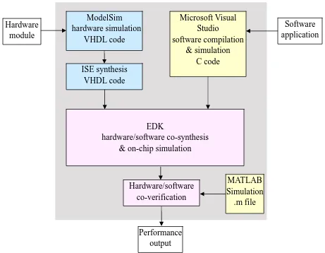
Figure 3.3 Design flow for FPGA-based HW/SW co-design systems
In HW/SW co-designs, the application is partitioned into soft core and hardware modules.
The software applications are developed and simulated in C language by Microsoft Visual Studio
[29]. The hardware modules are first described in VHDL language, and simulated in Mentor
Graphics ModelSim [30] at RTL level. Then they are synthesized in Xilinx ISE [31] software
environment and translated into electronic hardware circuits to be mapped on chosen FPGA.
Xilinx EDK [32] tool is used to merge the hardware and software designs together, and it is a
co-design process. As shown in Figure 3.4, the system window is used to design the SoC
architecture, where versatile hardware modules can be attached to the embedded processor with
certain address allocation and I/O assignments. After that the software application is developed
in the Application window along with the interface between the software and hardware modules.
The on-chip simulations for the whole system can also be conducted within the EDK tool.
Figure 3.4 Xilinx EDK workplace
At last, the results from the HW/SW co-design are verified with the MATLAB software
simulations. In the MIMO lattice decoder designs, the performances of decoding rate, FPGA
Figure 3.4 XUP Virtex-II Pro developing board [17]
Xilinx XUP Virtex-II Pro developing board is chosen as the target board for the
implementations of lattice decoders. It consists of a high performance XC2VP30 FPGA
surrounded by a comprehensive collection of peripheral components that can be used to create a
complex system. The FPGA device can be configured by several methods including external
parallel port interface, USB cable or internal CompactFlash storage media [33]. One or more MB
soft cores can be implemented by configuring a group of logic cells inside the FPGA chip.
Efficient architecture of aforementioned two sphere lattice decoders is explored in the next
Chapter 4
Hardware/software architecture for MIMO Sphere decoders
This chapter presents HW/SW co-design architecture for two MIMO sphere decoding
algorithms. A coarse-gain partition of both algorithms is discussed first. Then three levels of
parallel structures are explored to generate an efficient HW/SW architecture to improve the
system performance. The co-design architecture is prototyped on the Xilinx Virtex-II Pro
developing board.
4.1 Partitioning of the sphere decoding algorithms
In our AV and VB sphere decoding algorithms, the basis reduction is generally performed to
reduce the complexity of the decoding procedure, which transforms the lattice generation matrix
into a triangular matrix. This process is called preprocessing that involves matrix factorization
operations such as QR or Cholesky decompositions and matrix inversions. These complex matrix
manipulations are difficult and not efficient to be mapped directly onto FPGAs. Fortunately, in
MIMO wireless communications, the preprocessing stage of the sphere decoders does not need
to be updated frequently. Generally, the channel matrix H can be assumed to be static during the
transmission of one frame length of data signals. Therefore the preprocessing of lattice
generation matrix only needs to be executed once for a certain time period (typically 10 ms). The
MB soft processor on Virtex-II Pro FPGA running at about 100 MHz is able to complete the
preprocessing task timely. For this reason, the basis reduction operations for both AV and VB
searching procedure needs to be executed for every received signal vector. This iterative
procedure is very time consuming if implemented sequentially in soft processor. Furthermore the
decoding rate of the sphere decoder is determined by the average completion time of the
searching procedure. Thus it is desirable to put the sphere searching procedure directly into
FPGA hardware circuits. The gate level implementations on FPGA can greatly accelerate the
computationally intensive functions involved in the decoding procedure. Because of supporting
parallelism, some of the decoding calculations can be executed concurrently if no data flow
dependency lies among them. Once an efficient architecture is explored, the FPGA-based
implementation can extraordinarily speed up the decoding procedure of the sphere decoders. In
addition to the performance gain, FPGA device also provides the flexibility to reconfigure the
system to accommodate any changes of the MIMO systems including number of antennas,
modulation schemes, and etc.
Based on the analysis above, a straightforward coarse-gain partition is applied to the AV and
VB decoding algorithms to build up the HW/SW co-design architecture, which includes a soft
processor, customized hardware module(s), and a shared peripheral bus between them for data
communication. As shown is Figure 3.1, the channel matrix preprocessing is implemented in the
embedded MB soft core, and the decoding procedure is mapped onto FPGA hardware modules.
The preprocessing results (the upper or lower triangular matrix) are transferred from the MB to
the hardware modules periodically through the OPB interface, which is synchronous to MB
processor and can achieve a high data transfer rate. Subsequently, three levels of parallel
while maintaining the same BER performance.
4.2 Processor level parallelism
MicroBlaze (Preprocessing) OPB interface
Customized Hardware
Figure 4.1 Architecture of the processor level parallelism
The HW/SW co-design architecture for both AV and VB algorithms is illustrated in Figure
4.1. The preprocessing part including matrix factorization and inversion is programmed on MB
soft processor for both algorithms. The lattice searching procedure is implemented in customized
hardware modules to improve the decoding rate. The OPB interface is used to transfer data
between them. The processor level parallelism refers to the concurrent execution of the
preprocessing stage and the decoding procedure. And multiple decoding blocks can be mapped
onto the FPGA. This is feasible because all signals received within the same frame length are
decoded using the same triangular matrix decomposed by the preprocessing unit. Thus multiple
received vectors can be decoded simultaneously. The maximum number of the customized
modules that can be implemented is determined by the size of the hardware core and the
available resources of chosen FPGA.
To evaluate the performance gain brought by the processor level parallelism, t is defined as (Decoding)
the execution time of the preprocessing part, and td is defined as the average execution time to
decode one received vector. Then the system architecture with 1 MB processor and N customized
hardware modules can achieve a speedup factor of:
) / , max(t t L N
L t t S
d p
d p f
+
= Eq 4.1
where L is the number of received vector per frame length. There exists a slight overhead before
starting a new searching procedure in hardware modules, because the received vectors need to be
manipulated for different hardware modules based on the basis reduction schemes in MB soft
processor. This overhead is not significant because only the multiplication of a 1×N vector with
an N×M orthogonal matrix is involved. Furthermore, instead of execution in MB soft core, if
this multiplication is partitioned into each hardware module, this kind overhead can be almost
ignored because of the parallel executions in FPGA. Based on the EDK synthesis results shown
in Chapter 5, the XC2VP30 FPGA can accommodate 4 hardware decoders for the AV algorithm
and 3 hardware decoders for the VB algorithm in parallel to accelerate the decoding speed.
4.3 Complex constellation parallelism
In wireless communications, the transmitted signals are often modulated using the complex
quadrature amplitude modulation scheme. If this is the case, the MIMO channel matrix H
becomes an M×N complex matrix, and the received signal y and the transmitted signal u
becomes 1×N and 1×M complex vectors respectively. In this subsection, the MIMO systems
with the same number of transmit and receive antennas (M=N) are considered to achieve the
4.3.1 Conventional 2M-dimensional search method
Generally, the MIMO system can be described as:
y =uH +n Eq 4.2
The sphere decoders search the closest lattice point in a specified order as discussed in chapter 2.
But in the complex constellation case, the admissible order in each searching layer can not be
easily specified because the examining index in each layer becomes a complex number. A
solution for this problem is to linearly transform Eq 4.2 into [35]:
T T T n n H H H H u u y y ⎥ ⎦ ⎤ ⎢ ⎣ ⎡ ℑ ℜ + ⎥ ⎦ ⎤ ⎢ ⎣ ⎡ ℜ ℑ − ℑ ℜ ⎥ ⎦ ⎤ ⎢ ⎣ ⎡ ℑ ℜ = ⎥ ⎦ ⎤ ⎢ ⎣ ⎡ ℑ ℜ } { } { } { } { } { } { } { } { } { } { Eq 4.3
where and represent the real part and imaginary part of a complex number x. Thus
the M-dimensional complex decoding problem can be solved via decomposing the complex
matrix into an equivalent 2M-dimensional (2M-D) real matrix as shown in Eq 4.3. }
{x
ℜ ℑ{x}
Thus the inputs of the sphere decoder become a 2M-dimensional channel matrix and a 1×2M
received vector. While this method provides a possible approach to the complex MIMO systems,
the searching space is greatly enlarged by the doubled dimension. 2M layers are involved in the
decomposed channel matrix, thus significantly increases the number of iterations during the
closest lattice point searching procedure. Figure 4.2 shows the number of states visited as the
dimension of MIMO channel matrix grows for the AV algorithm. Number of states visited is
increased greatly when the dimension of MIMO system doubles. And as the number of states
visited is an important factor of the decoding rate, the data throughput of the MIMO decoder will
the complex lattice into a 2M-dimensional real lattice ignores the orthogonal feature of real and
imaginary parts of a complex system and the symmetry of the QAM constellation, thus reducing
the possibility of parallel implementations on FPGA. Consequently, the conventional 2M-D
method is not suitable for FPGA implementations.
Figure 4.2 Number of states visited vs. number of antennas
An efficient two M-dimensional (two M-D) transform method is mathematically derived for
an alternative solution to the complex MIMO decoders. And the simulation results are presented
to verify its performance.
4.3.2 Two M-dimensional search method
The idea of the two M-D transform method is to decompose the M-dimensional complex
MIMO decoding problem into two independent M-dimensional real problems. Each decomposed
subsystem only contains the real part or imaginary part of the transmitted signals. Hence the
complex lattice decoding problem is solved by decoding the real part and imaginary part of the
Eq 4.3 can be rewritten into the following two equations by multiplying out the matrix H and
vector u:
} { } { } { } { } { }
{y =ℜ u ℜ H −ℑ u ℑ H +ℜ n
ℜ Eq 4.4
} { } { } { } { } { }
{y =ℜ u ℑ H +ℑ u ℜ H +ℑ n
ℑ Eq 4.5
By calculating Eq4.4 + Eq4.5*ℜ−1{H}*ℑ{H}, we can get:
} { } { } { } { }) { } { } { } { }( { } { } { } { } { 1 1 1 H H n n H H H H u H H y y ℑ ℜ ℑ + ℜ + ℑ ℜ ℑ + ℜ ℜ = ℑ ℜ ℑ + ℜ − − − Eq 4.6
Similarly, by solving Eq4.4*ℜ−1{H}*ℑ{H}−Eq4.5, we have:
} { } { } { } { }) { } { } { } { }( { } { } { } { } { 1 1 1 H H n n H H H H u H H y y ℑ ℜ ℜ − ℑ + ℑ ℜ ℑ + ℜ ℑ = ℑ ℜ ℜ − ℑ − − − Eq 4.7
To simplify these equations, we denote the following terms:
} { } { } { } { } { } { } { } { } { } { } { } { } { } { } { } { } { } { } { } { 1 2 1 1 1 1 2 1 1 H H n n n H H n n n H H H H S H H y y y H H y y y ℑ ℜ ℜ − ℑ = ℑ ℜ ℑ + ℜ = ℑ ℜ ℑ + ℜ = ℑ ℜ ℜ − ℑ = ℑ ℜ ℑ + ℜ = − − − − − Eq 4.8
By substituting Eq 4.8 into Eq 4.6 and Eq 4.7, we get:
1 1 {u}S n
y =ℜ + Eq 4.9
2 2 {u}S n
y =ℑ + Eq 4.10
Thus the complex lattice decoding problem of Eq 4.2 can be decomposed into two
independent M-dimensional real decoding problems shown in Eq 4.9 and Eq 4.10. This
transformation is well suited for FPGA-based implementations because the real and imaginary
constellation parallelism in the sphere decoder architecture. Since the number of states visited for
each decoding part remains the same as an M-dimensional real system, this method can
significantly improves the decoding rate for a MIMO system with complex modulation scheme.
Of cause there exist some overheads to achieve this performance gain, because the matrix S,
vectors y1 and y2 in Eq 4.8 need to be calculated before the preprocessing and lattice
searching procedure starts. But by partitioning the calculation of S into MB soft core, and y1
and y2 into FPGA hardware modules, this parallelism is still able to meet the preprocessing
time requirement and greatly improve the throughput of the sphere decoder. The architecture of
the complex constellation parallelism is illustrated in Figure 4.3, as the R-decoder and I-decoder
denote for the real part and the imaginary part decoders respectively.
MicroBlaze (Preprocessing) OPB interface
Hardware Decoder
R-decoder I-decoder
Figure 4.3 Architecture of complex constellation parallelism
The transformed matrix S is calculated in MB soft processor. Then it is decomposed in the
preprocessing stage to generate the triangular matrix. The results are transferred to hardware
decoder along with an intermediate matrix ℜ−1{H}ℑ{H}, which is used to calculate y1 and
2
y as in Eq 4.8. At last the vectors y1 and y2 are decoded concurrently in the R-decoder and
4.3.3 Simulation validation
After mathematically deriving the two M-D transform method for complex MIMO decoders,
the MATLAB simulations are carried out to validate its BER performance with the conventional
2M-D method. 4×4 MIMO decoders with 16-QAM modulation scheme are simulated for both
AV and VB algorithms. The BER performances are compared between the aforementioned two
decoding transformations at different SNRs. The results are presented in Figure 4.4.
Figure 4.4 Comparisons of BER performances of two transformation methods
According to the simulation results, the two M-D transform method results in a slight
degradation in BER performance for both AV and VB algorithms. This is because some
distortions have been involved by this two M-D method to improve the decoding efficiency. In
the basis reduction and 2M-D transformations, the original channel matrix and the transformed
matrix are identical because one can be obtained from the other through scaling, rotation, and
the sphere decoding algorithms if the same signal constellation is used. Unlike these identical
transforms, the two M-D transform reduces the points in the lattice structure from 2MQ to 2*2MQ/2
by Eq 4.9 and 4.10, where M and Q denote for the number of transmit antennas and the number
of bits used to represent a symbol in the signal constellation. Although only basic transforms are
used, there are still some distortions involved by this nonlinear two M-D transformation. And
Figure 4.4 shows that the VB decoder suffers a bigger distortion than the AV decoder. But even
in the VB decoder, the two M-D method brings only about 1 dB degradation in BER
performance compared with the 2M-D method. Furthermore, by considering the reduction of the
number of states visited, as shown in Figure 4.5, it is clear that the proposed two M-D method
can considerably accelerate the decoding procedure and meanwhile keeps the BER performance
within an acceptable degradation range.
4.4 State level parallelism
To further improve the decoding speed, a state level parallelism is developed based on the
data flow dependency analysis between all the states shown in Figure 2.2 and 2.4. A finite state
machine (FSM) is designed to control the transitions among these states. This state level
parallelism is implemented in the FPGA hardware modules.
4.4.1 Data flow dependency analysis
There are three states involved in the decoding procedure as described in the step by step
demonstration in Figure 2.4 for the AV algorithm. Figure 4.6 shows the data dependency between
all possible state transition pairs. State A is dependent on both states B and C if the search
procedure switches to A from B or C, because the orthogonal distance d calculated in B or C is
used to upgrade the layer index ui in State A. Similarly, State A is self dependent. State B has no
dependency on A because these two states work on different search dimensions if B follows A
during the decoding procedure. For the same reason State C is not dependent on any other states
that could jump to C. Based on the data flow dependency, the possibility of the parallelism
among these three states is found as: A || B, A || C, B || C, C || C. These conditions are used to
implement the state level parallelism for the AV algorithm.
B
C A
Similar to the AV algorithm, the data flow dependency for the VB algorithm can be drawn in
Figure 4.7. Because of high data dependency among the decoding procedure, only State C can be
executed simultaneously with states B or C in this algorithm, which is summarized as: B||C, C||C.
B A
Figure 4.7 Data flow dependency graph of VB algorithm
4.4.2 Hardware architecture of state level parallelism
Depending on the data flow dependency analysis above, multiple states can be executed
concurrently in the hardware decoding modules. As an example, Figure 4.8 presents the
hardware architecture of state level parallelism for the AV decoder. An FSM is designed as a
central unit to control the state transitions and synchronization between them. For a 4-antenna
MIMO system, five hardware state modules are created, with one for each state and other two
duplicated C states. This is because up to three State Cs can be executed in parallel based on the
data flow analysis and experimental results. For instance, when the current state is B, FSM
enables not only State B but also all three State C models. The results from these modules can be
directly used if this State B is followed by multiple C states. A data buffer unit is used to
temporally store the data during the decoding procedure.
C D
Dependent

![Figure 3.2 Xilinx FPGA structure [28]](https://thumb-us.123doks.com/thumbv2/123dok_us/8937377.1848315/35.612.76.540.79.297/figure-xilinx-fpga-structure.webp)
![Figure 3.4 XUP Virtex-II Pro developing board [17]](https://thumb-us.123doks.com/thumbv2/123dok_us/8937377.1848315/38.612.104.510.74.434/figure-xup-virtex-ii-pro-developing-board.webp)