Copyright © 2013 IJECCE, All right reserved
Efficient Design of Half Adder and Half Subtractor
Using New SN Reversible Gate
Nayana D. K.
Department of Electronics and Communication, REVA Institute of Technology, Bangalore, India
Email: [email protected]
Sujatha B. K.
Department of Telecommunication Engineering, M S Ramaiah Institute of Technology, Bangalore, India
Email: [email protected]
Abstract - In the recent years, the reversible logic design attracting more interest due to its low power consumption. Reversible logic is very important in low power circuit design. Reversible logic has extensive applications in quantum computing, low power VLSI design, nano technology and optical computing. The classical set of gates such as AND, OR and EXOR are not reversible. This paper proposes a new 3 * 3 reversible gate called“SN “reversible gate. The proposed gate is used to design efficient adder and subtractor units. The proposed gate can be used to implement AND, XOR, XNOR and NOT gates. It is demonstrated that the adder/subtractor architectures designed using the proposed gate are much better and optimized, in terms of reversible gates and garbage outputs. Thus this paper provides the initial threshold to building of more complex system which can be execute more complicated operations using reversible logic.
Keywords - Reversible Logic, Garbage Output, New SN Reversible Gate, Reversible Binary Half Adder/Half Subtractor.
I. I
NTRODUCTIONReversible logic is emerging as a promising computing paradigm with applications in emerging technologies such as quantum computing, quantum automata, optical computing, etc.([3]- [8]).Researchers like Landauer have shown that for irreversible logic computations, each bit of information lost, generates kTlog2 joules of heat energy, where k is Boltzmann’s constant and T is the absolute temperature at which computation is carried out[9]. Bennett showed that kTln2 energy dissipation would not occur, if a computation is carried out in a reversible way [10], since the amount of energy dissipated in a system bears a direct relationship to number of bits erased during computation. The gate does not loose information is called
reversible. A reversible gate has the equal number of
inputs and outputs and one-to-one mappings between input vectors and output vectors; so that, the input vector states can be always uniquely reconstructed from the output vector states. Also in the synthesis of reversible circuits direct fan-out is not allowed as one-to-many concept is not reversible. However fan-out in reversible circuits is achieved using additional gates [1].
One of the main constraints in reversible logic is to minimize the number of reversible gates used and garbage output produced. Every gate output that is not used as input to other gate or as a primary output is called garbage. Garbage output refers to the output that is not used for further computations. A heavy price is paid for every garbage bit, if the garbage bit is left unattended. In
reversible logic, fan-out of any gate output is not allowed; every output can be used only once. A reversible gate with
x inputs and x outputs is known as x*x gate. For instance,
the Feynman gate described by the equation P=A,Q=A B is reversible, as it can be seen in its truth table (described later), because for each combination of output signals P, Q there is one combination of input signals A, B. A reversible circuit should be designed using minimum number of reversible logic gates. But there are many parameters for determining the complexity and performance of circuits.
The number of Reversible gates: The number of reversible gates used in circuit.
The number of constant inputs: This refers to the number of inputs that are to be maintained constant at either 0 or 1 in order to synthesize the given logical function.
The number of garbage outputs: This refers to the number unused outputs present in a reversible logic circuit. One cannot avoid the garbage outputs as these are very essential to achieve reversibility.
Quantum Cost: This refers to the cost of the circuit in terms of the cost of a primitive gate. It is calculated knowing the number of primitive reversible logic gates required to realize the circuit [1].
The paper is organized as follows. Section 2 deals with the introduction of basic reversible gates. Section 3 deals with the proposed SN reversible gate. Section 4 deals with the designs of reversible adder and subtractor using proposed SN gate. Section 5 deals with the result analysis of the proposed design and Conclusions are contained in section 6. The references are listed in section 7.
II. R
EVERSIBLEL
OGICG
ATESThere are many universal reversible gates [2]. Some of the important reversible gates are introduced:
There is only one 1*1 reversible logic gate, which is inverter. This gate is important since it does not introduce garbage outputs.
Fig.1. Feynman Gate Table I: Truth table of Feynman Gate
A B P Q
0 0 0 0
0 1 0 1
1 0 1 1
1 1 1 0
There exist 40,320 (=8!) 3*3 reversible logic gates [2]. Toffoli Gate is a 3*3 two-through reversible gate as shown in Fig. 2 [3]. The corresponding truth table is shown in Table II. Two-through means two of its outputs are same as the inputs with the mapping (A, B,C) to (P=A,Q=B, R=A.BC), where A,B,C are the inputs and P,Q,R are the outputs, respectively [11].
Fig.2: Toffoli Gate
Table II: Truth table of Toffoli Gate
A B C P Q R
0 0 0 0 0 0
0 0 1 0 0 1
0 1 0 0 1 0
0 1 1 0 1 1
1 0 0 1 0 0
1 0 1 1 0 1
1 1 0 1 1 1
1 1 1 1 1 0
Peres Gate is a 3*3 reversible gate as shown in Fig. 3. The corresponding truth table is shown in Table III. The inputs are mapped to outputs as (P=A, Q=AB, R=A.B C), where A, B, C are the inputs and P,Q,R are the outputs, respectively [1].
Fig.3. Peres Gate
Table III: Truth table of Peres Gate
A B C P Q R
0 0 0 0 0 0
0 0 1 0 0 1
0 1 0 0 1 0
0 1 1 0 1 1
1 0 0 1 1 0
1 0 1 1 1 1
1 1 0 1 0 1
1 1 1 1 0 0
III. P
ROPOSED3*3 R
EVERSIBLEG
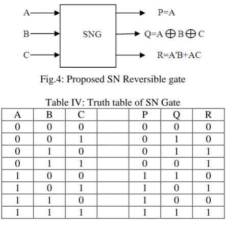
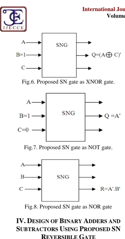
ATEIn this paper, a 3*3 one through reversible gate called SN gate “SNG” is proposed. The proposed reversible SNG gate is shown in fig.4. The corresponding truth table of the gate is shown in table IV. The inputs are mapped to outputs as (P=A, Q=ABC, R= A'B+AC). It can be verified from the truth table that the input pattern corresponding to a particular output pattern can be uniquely determined. The proposed SNG gate can implement all Boolean functions. Fig.5 shows the implementation of the proposed gate as XOR and AND function. Fig.6 shows the implementation of the proposed gate as XNOR function. Fig.7 shows the implementation of the proposed gate as NOT function. Fig.8 shows the implementation of the proposed gate as NOR function with input B passed in complemented form by using a NOT gate. Since, the NOR gate is a universal gate and any Boolean function can be implemented through it. Hence, the proposed gate can be used to implement any Boolean function[12]. One of the prominent functionality of the proposed gate is that it can work singly as a reversible half subtractor unit.
Fig.4: Proposed SN Reversible gate Table IV: Truth table of SN Gate
A B C P Q R
0 0 0 0 0 0
0 0 1 0 1 0
0 1 0 0 1 1
0 1 1 0 0 1
1 0 0 1 1 0
1 0 1 1 0 1
1 1 0 1 0 0
1 1 1 1 1 1
It is possible to realize the proposed SN gate from 2 Feynman gate and 1 Freadkin gate. Thus the proposed quantum cost of SN gate will be quantum cost of 2 Feynman gate + quantum cost of 1 Freadkin gate = 7.
Copyright © 2013 IJECCE, All right reserved Fig.6. Proposed SN gate as XNOR gate.
Fig.7. Proposed SN gate as NOT gate.
Fig.8. Proposed SN gate as NOR gate
IV. D
ESIGN OFB
INARYA
DDERS ANDS
UBTRACTORSU
SINGP
ROPOSEDSN
R
EVERSIBLEG
ATEWe used proposed NS reversible gate to design the binary adders such as half adder and full adder. The same SNG is used to design the binary subtractors such as half subtractor and full subtractor.
A. Half Subtractor
Let A and B are two binary numbers. The half subtractor performs A-B operation. Table V shows the truth table of the half subtractor. From the truth table the output Diff=AB and Bout=A'.B. Hence, half subtractor can be designed using only one proposed SN reversible gate as shown in fig.9.
Table V: Truth table of Half Subtractor
A B Diff Bout
0 0 0 0
0 1 1 1
1 0 1 0
1 1 0 0
Fig.9. Proposed SN gate working as a Reversible Half Subtractor.
A number of reversible half subtractors were proposed in ([13]-[16]). The reversible half subtractor circuit in [13] requires three reversible gates (one 2*2 Feynman gate and two 3*3 SSG gate) and produces four garbage outputs. The reversible half subtractor circuit in [14 of design1] requires three reversible gates (one 4*4 BVF gate and two 3*3 BJN gate) and produces four garbage outputs. The reversible half subtractor circuit in [14 of design 2] requires four reversible gates (two 2*2 Feynman gate, one 3*3 Peres gate and one 3*3 BJN gate) and produces five garbage outputs. The design in [15] requires three reversible gates (one 4*4 BVF gate and two 3*3 MTG gate) and produces three garbage outputs. The design in [16] requires two reversible gate and produces three garbage outputs. The proposed half subtractor using SN gate in fig.9 requires only one reversible gate and produces only one garbage output. Hence, the half subtractor design in fig.9 using SN gate is better than previous half subtractor designs of ([13]-[16]) in terms of both the number of reversible gates and the number of garbage outputs. A comparative result is shown in table VI.
Table VI: Comparative Results of Different Half Subtractor Circuits.
No. of Gates
No. of Garbage Outputs
Proposed Circuit 1 1
Existing Circuit[13] 3 4
Existing Circuit[14 of design 1]
3 4
Existing Circuit[14 of design 2]
3 4
Existing Circuit[15] 3 3
Existing Circuit[16] 2 3
B. Half Adder
Let A and B are two binary numbers. The half adder performs A+B operation. Table VII shows the truth table of the half adder. From the truth table the output Sum=A B and Cout=A.B. Hence, half adder can be designed using only one proposed SN reversible gate as shown in fig.10.
Table VII: Truth table of Half Adder
A B Sum Cout
0 0 0 0
0 1 1 0
1 0 1 0
1 1 0 1
A number of reversible half adders were proposed in ([13]-[15]). The reversible half adder circuit in [13] requires three reversible gates (one 2*2 Feynman gate and two 3*3 SSG gate) and produces four garbage outputs. The reversible half adder circuit in [14 of design1] requires three reversible gates (one 4*4 BVF gate and two 3*3 BJN gate) and produces four garbage outputs. The reversible half adder circuit in [14 of design 2] requires two reversible gates (one 3*3 Peres gate and one 3*3 BJN gate) and produces two garbage outputs. The design in [15] requires three reversible gates (one 4*4 BVF gate and two 3*3 MTG gate) and produces three garbage outputs. The proposed half adder using SN gate in fig.10 requires only one reversible gate and produces only one garbage output. Hence, the half adder design in fig.10 using SN gate is better than previous half adders designs of ([13-[15]) in terms of both the number of reversible gates and the number of garbage outputs. A comparative result is shown in table VIII.
Table VIII: Comparative Results of Different Half Adder Circuits.
No. of Gates
No. of Garbage Outputs
Proposed Circuit 1 1
Existing Circuit[13] 3 4
Existing Circuit[14 of design 1]
3 4
Existing Circuit[14 of design 2]
2 2
Existing Circuit[15] 3 3
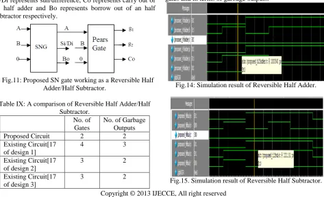
C. Half Adder/Half Subtractor
Reversible half Adder/half Subtractor is designed using two reversible gates of which one 3*3 proposed SN reversible gate and one 3*3 Peres gate is shown in fig.11.The number of garbage output is two. In fig.11. Si/Di represents sun/difference, Co represents carry out of an half adder and Bo represents borrow out of an half subtractor respectively.
Fig.11: Proposed SN gate working as a Reversible Half Adder/Half Subtractor.
Table IX: A comparison of Reversible Half Adder/Half Subtractor.
No. of Gates
No. of Garbage Outputs
Proposed Circuit 2 2
Existing Circuit[17 of design 1]
4 3
Existing Circuit[17 of design 2]
3 2
Existing Circuit[17 3 2
Thus, SN gate implements the reversible half adder/half subtractor with the help of Peres gate. Totally we have used two reversible gates and the circuit produces two garbage outputs. A comparison of the reversible half adder/half subtractor is shown in Table IX. We have done our comparison with the designs in [17] as to the best of our knowledge; it is the only work in literature describing the designing of reversible half adder/half subtractor.
The existing design in literature [17] is implemented with four reversible gates (two 2*2 Feynman gate, two 3*3 Fredkin gate) and produces three garbage outputs. The reversible half adder/half subtractor circuit [17 of design 2 and design 3] requires here reversible gates (two 2*2 feynman gate and one 3*3 TR gate) and produces two garbage outputs. The proposed half adder/half subtractor using SN gate in fig.11 requires two reversible gates and produces two garbage outputs. Hence, the half subtractor design in fig.11 using SN gate is better than previous half adder/half subtractor designs of [17] in terms both the number of reversible gates and the number of garbage outputs.
V. S
IMULATIONR
ESULTSReversible Half Adder, Half Subtractor, Half Adder/Half Subtractor are implemented using Verilog code and Simulated using Modelsim Simulator. The overall logic is implemented using Structural style of Modelling and simulation results are shown in Figure 14, 15 and 16 respectively. From Table 6 it is proved that proposed Half Subtractor is better in terms of number of reversible gates and in terms of garbage outputs. Table 8 it is proved that proposed Half Adder is better in terms of number of reversible gates and in terms of garbage outputs. Table 9 it is proved that proposed Half Subtractor / Half Adder is better in terms of number of reversible gates and in terms of garbage outputs.
Fig.14: Simulation result of Reversible Half Adder.
Copyright © 2013 IJECCE, All right reserved Fig.16: Simulation result of Reversible Half Adder/Half
Subtractor.
VI. C
ONCLUSIONThe focus of this work is the proposal of new reversible 3*3 SN gate. The proposed SN gate is being used to perform different operations such as AND, XOR, etc., and is used to design the Arithmetic circuits such as half adders and half subtractors, and half adder/half subtractor. It is proved that all the adder and subtractor architectures proposed in this paper are better in terms of reversible gates and in terms of garbage outputs, which plays an important role in reversible logic design. Thus, the paper provides the initial threshold to build more complex systems which can be execute more complicated operations. The proposed reversible gate forms the basis for the design of ALU.
R
EFERENCES[1] Prof. Sujata S. Chiwande, Prashant .R. Yelekar,”Introduction to Reversible Logic Gates & its Application”, 2nd national Conference on Information and Communication Technology–
2011, Proceedings published in International Journal of Computer Applications.
[2] Hafiz Md. Hasan Babu, Md. Rafiqul Islam, Ahsan Raja Chowdhury, Syed Mostahed Ali Chowdhury,”Reversible Logic Synthesis for Minimization of Full Adder circuit”, Proceedings of the Euromicro Symposium on Digital System Design, EEE Computer Society,-7695-2003-0/03.
[3] A.N.Al-Rabadi, Reversible Logic Synthesis: From Fundamentals to Quantum Computing, Springer-verlag, Network, First edition, 2004.
[4] V.Vedral, A.Barenoand, A.Ekert, “Quantum Network for Elementary Arithmetic Operations”, arXiv:quant-ph/ 95110118vl.(Nov.1995).
[5] H.Thapliyaland, N Ranganatham, “Reversible Logic Based Concurrently Testable Latches for Molecular QCA”, To appear
IEEE Trans. On Nanotechnology, 2009.
[6] H.Thapliyal and N.Ranganatham,”Testable Reversible Latches for Molecular QCA”, Proc. Of the 8th Intl. Conf. On Nanotechnology, Arlington, Tx, Aug-2008, pp.699-702. [7] H.Thapliyal and N.Ranganatham, “Conservative QCA Gate
(CQCA) for Designing Concurrently Testable Molecular QCA Circuits”, Proc. Of the 22ndIntl. Conf. On VLSI Design, New Delhi, India, Jan 2009, pp. 511-516.
[8] X.ma,J.Huang, C.Metra, F.Lombardi, “Reversible Gates and Testablity of One Dimensional Arrays of Molecular QCA”, Springer Journal of Electronic Testing, vol.24, No.1-3, pp.297-311, Jan 2008.
[9] R.Landauer, “Irreversibility and Heat Generation in the Computational Process”, IBM Journal of Research and Development, 5, pp.183-191, 1961.
[10] C.H.Bennett, “Logical Reversibility of Computation”, IBM Journal of Research and Development, pp.525-532, Nov.1973.
[11] Himanshu Thapliyal, Nagarajan Ranganathan, “Design of Efficient Reversible Binary Subtractors Based on a New Reversible Gate”, IEEE Computer Society Annual Symposium
on VLSI, pp.229-234, Nov.2009.
[12] Himanshu Thapliyal, M.B.Srinivas, “A New Reversible TSG Gate and its Applications for Designing Efficient Adder Circuits”,Proceedings of the 7th International Symposium on Representations and Methodology of Future Computing Technologies (RM 2005), Tokyo, Japan, 2005.
[13] N.Srinivas Rao, P.Satyanarayana, “A Novel Reversible Gate and its Applications”,Intl. Journal of Engineering and Technology, Vol.2,No.7,pp.1318-1323, July 2012.
[14] Divyansh Mathur, Arti Saxena, Abneesh Saxena,“Arthmetic and Logic Unit Designing using Reversible LogicGate”,Intl. Journal of Recent Technology and Engineering(IJRTE), Vol.1, Issue-6, pp.157-160, Jan.2013.
[15] Jayashree H.V., Nagamani A.N., Bhagyalakshmi.H.R., “Modified Toffoli Gate and its Applications in Designing Components of Reversible Arithmetic and Logic Unit”, Intl. Journal of Advanced Research in Computer Science and Software Engineering, Vol.2, Issue-7,pp.207-210, July-2012. [16] H.Thapliyal, M.B.Srinivas and H.R.Arabnia,“Reversible Logic
Synthesis of Hale,Full and Parallel Subtractors”,Proc.of the Intl. Conf. On Embedded Systems and Applications, LasVegas, pp.165-181, june 2005.
[17] Rangaraju H.G., Venugopal U, Muralidhara K.N, Raja K.B., “Low Power Reversible Parrallel Binary Adder/Subtractor”, Academy & Industry Research Collaboration Center (AIRCC), Year 2010.
[18] Md.M.H.Azad Khan, “Design of Full Adder withreversible Gates”, Intl. Conference on Computer and Information Technology, Dhaka, Bangladesh, 2002, pp.515-519.
[19] J.W.Bruce, M.A.Thomton,L.Shivakumaraiah, P.S.Kokate and X.Li, “Efficient Adder Circuits Based on a Conservative Logic Gate”,Proc. of the IEEE Computer Society Annual Symposium on VLSI, April 2002, Pitsburgh, PA, USA,pp.83-88.
A
UTHOR’
SP
ROFILENayana D. K.
is a Assoc. Prof. In the Department of Electronics and Communication Engineering, REVA Institute of Technology and Management, Visvesvaraya Technological University, Belgaum, Karnataka, India. She obtained her Bachelor degree in Electronics and Communication Engineering from Mysore University, Karnataka, India in 1994 and Master of Technology degree in Digital Electronics and Advanced Communication from Mangalore University, Karnataka, India in 1998. She is pursuing Ph.D in Electronics and Communication Engineering, Jain University, Bangalore, Karnataka, India. Her research interest includes VLSI Design and Wireless Communication.