Please cite this article as: M. Gholami, R
International Journal of Engineering
J o u r n a l H o m e p a g e : w w w . i j e . i rM. Gholami*a, R. Binaeib,M. Gholamnia Roshanb
a Faculty of Engineering and Technology, University of Mazandaran, Babolsar, Iran
b Department of Electrical and Computer Engineering, Mazandaran Institute of Technology, Babol, Iran
P A P E R I N F O
Paper history: Received 28 April 2019
Received in revised form 15 December 2019 Accepted 16 Januray 2020
Keywords:
Quantum Cellular Automata Quantum-dot Cellular Automata Phase-frequency Detector Phase Detector Power Consumption
A B S T R A C T
The electronic industry has grown vastly in recent years, and researchers are trying to minimize circuits delay, occupied area and power consumption as much as possible. In this regard, many technologies have been introduced. Quantum Cellular Automata (QCA) is one of the schemes to design nano-scale digital electronic circuits. This technology has high speed and low power consumption, and occupies
very little area. Phase-locked loops (PLLs) and delay-locked loops (DLLs)are blocks that are commonly
used in telecommunication applications. One of the most important parts in DLL and PLL is the phase-frequency detector. Therefore, the design of this circuit in QCA technology is of great importance. In this paper, two new phase-frequency detectors sensitive to falling and rising edge have been introduced
in QCA technology. Both of the designs are composed of 104 cells; occupy only 0.13 μm2 of an area and
1.5 QCA clock cycles latency. The designs are in one layer and all the inputs and outputs are available to be used by another circuit.
doi: 10.5829/ije.2020.33.02b.11
1. INTRODUCTION1
With advancement of CMOS technology, many efforts have been made for increasing the speed of this technology along with decreasing the dimensions. These efforts have reached a level where it can be said that the technology has reached its end, and much progress cannot be expected. Furthermore, miniaturization has caused some malfunctions in circuits operation. Quantum dot Cellular Automata (QCA) technology is one of the nanotechnologies proposed to resolve issues including performance speed, occupied area and energy consumption of digital electronic circuits [1, 2]. This technology was first introduced by Lent and Togoa in 1993 [3].
The phase-frequency detector (PFD) is one of the most important electronics circuits, which plays an important role in commonly used communication circuit's design [4]. PFD is the main block in the phase-locked loops (PLLs) or delay-phase-locked loops (DLLs)
*Corresponding Author Email: [email protected] (M. Gholami)
architectures [5, 6]. This circuit recognizes the phase and frequency difference between two signals by examining them. This circuit can be used as a test circuit to compare the sent and received signals, and for detecting errors as well [7].
Metal Oxide Semiconductor )MOS) based PFDs have some challenges. For example, they suffer from low operating frequency, small capturing range, high values of power consumption, long reset path, static phase error and blind zones [7, 8]. Therefore, quantum dot cellular technology may be an option to solve these problems. In this paper two novel phase-frequency detector are
designed in quantum dot cellular automata
nanotechnology. Due to inherent abilities of QCA technology, the proposed PFDs show better performance in comparison with MOS-based PFDs in terms of energy consumption, operating frequency, area and reset path time.
The paper is organized as follow. Next section, describes the basic block diagram of PFD. Then Section
Novel Phase-frequency Detector Based on Quantum-dot Cellular Automata
Nanotechnology
3 illustrates the basics of QCA. The proposed circuits will be introduced in Section 4 and finally simulations and results will be shown in Section 5.
2. PHASE FREQUENCY DETECTOR
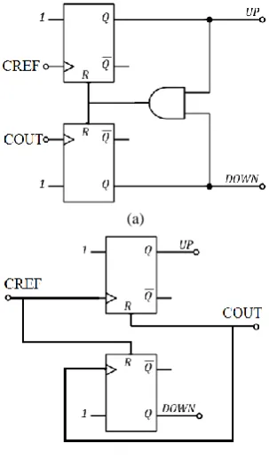
The phase-frequency detector circuit must be capable to detect the phase difference and frequency differences between the two signals practically. Figure1.a and Figure 1b show the conventional and modified block diagrams of PFD [7, 9].
Figure 1a shows a design that calculates the phase difference by analyzing circuit output, and controls them using reset pin of D flip-flops. The flip-flops inputs are connected to logic '1' and, if their clock is activated, the output would be logic '1'. When the second clock's rising edge comes, both flip-flops outputs are logic '1' for a moment. These outputs are connected to an AND gate and output of that gate is connected to the flip-flops reset. In this way, their reset is activated and the outputs of both circuits will be logic '0'. The time when the first signal is reached until the output be reset is called reset time.
In Figure 1b, the AND gate is removed and the circuit size is reduced as much as possible. In this scheme, in order to calculate clock signal differences, each input of flip-flops is connected to another flip-flop's reset input. In this case, for example when the second signal comes, it activates the reset of the first flip-flop and makes its output logica zero. Thus, the difference between the two
(a)
(b)
Figure 1. a) Conventional PFD, b) modified PFD
signals is obtained. It can be said that these two schemes have the same function, and their difference is the way that they reset the circuit when two signals come together.
One of the disadvantages of the scheme shown in Figure 1a is that once the second signal's rising edge is received, it needs a time equal to delay of each D flop and an AND gate for activating reset of the flip-flops. That means this architecture has much more reset path delay. This delay can cause responses to be invalid for small time duration, but the scheme shown in Figure 1b solves this problem and, when the two signals come together, each one activates another reset instantly. In the following, the principles of proposed circuits design in QCA technology are addressed, then the proposed circuit is introduced and simulated as well.
3. BASICS OF QCA
Unlike many technologies, QCA technology is not based on transistors, and in this technology circuits are designed using QCA cells. Each QCA cell (in two-dimensional mode) consists of four quantum areas and two electrons, which according to the Coulomb repulsion law, electrons can only be placed under two conditions in this point. These two conditions are conventionally chosen as logical one and zero, which are shown in Figure 2a. Despite the radius of influence around each electron, they can transfer their logical values if the QCA cells are spaced at appropriate distance. By using this, it is possible to design digital electronics circuits by appropriately placing QCA cells together.
The NOT and Majority gates are the most important gates that can be used to design all digital electronics circuits. These gates can be designed simply in QCA technology. In Figures 2b, 2c and 2d, examples of these two gates are shown.
When QCA cells are stimulated, they undergo a four-step operation (change, hold, release, and relax phases). Four clock phases are specified using these steps. Accordingly, for each QCA cell, a clock phase is specified which indicates the time of its operation, and each clock phase has a phase difference of 90° with the next and previous clock phases. The correct determination of these time zones plays a very important role in the correct circuit operation. These clock phases are shown in Figure 3.
4. PROPOSED PHASE-FREQUENCY DETECTORS
(a) (b)
(c)
(d)
Figure 2. a) Basic cells in QCA, b) Invetter in QCA, c)
Three-inputs majority gate in QCA, d) Five-input majority gate in QCA
Figure 3. Clock phases in QCA
proposed phase-frequency detectors are designed in QCA technology consistent with the block diagram in Figure 1b.
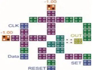
Based on this block diagram, D flip-flop plays the main role in circuit design. So far, many flip flops have been introduced in QCA technology, but the flip-flop used in the PFD should have the reset ability. In this paper, a new D latch is proposed that has the abilities of set and reset, and its schematic is shown in Figure 4. This
D latch has a few cells, small area, and small delay compared to similar circuits. This circuit consists of two three-input majority gates, a five-input majority gate, and a feedback. The input and output of circuit, each one are connected to one of the two three-input majority gates inputs. The input clock selects which one of those two gates outputs would be activated. The two gates outputs are connected to a five-input majority gate. This gate compares the values of two three-input majority gates outputs and the set and reset, and displays result in output. In the base circuit, in order to reduce the number of cells and the occupied area, a number of cells have been removed and clock phases are changed, which does not affect the output and flip-flop circuit's performance. A circuit is used to convert the latch to the flip-flop that examines the current and previous values of the signal and detects the edge (level to edge converter).
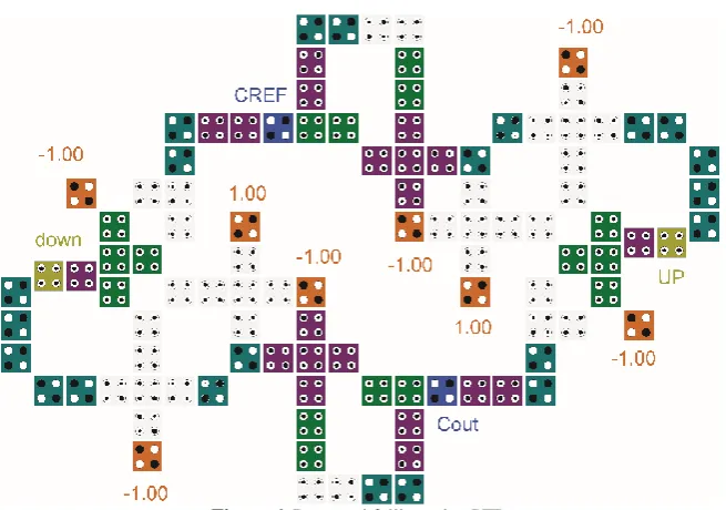
Using intended D latch structure along with edge conversion circuit, the desired D flip-flop is designed with set and reset abilities, and is used in the proposed PFD structures. Accordingly, the proposed phase-frequency detectors structures in QCA technology are shown in Figures 5 and 6, respectively, to reveal the difference between rising and falling edges. As is shown, the proposed circuits have two inputs called CREF and
COUT, which the two intended signals are applied to them
in order to determine the phase differences. Furthermore, there are two outputs called UP and DOWN, where the former indicates CREF signal is ahead of COUT, and the
laterindicates Cout signal is ahead of CREF. UP is logic
one during the time when CREF signal is ahead, DOWN
signal also performs this for COUT. Another important
point in these structures is the availability of inputs and outputs outside the circuit. This paper aims to design the proposed structures in terms of robustness. Next, the proposed circuits will be simulated to verify their performance.
5. SIMULATIONS AND RESULTS
To ensure the proposed circuit’s performance, two proposed structures are simulated in the QCADesigner
software [10, 11]. This software was established to simulate circuits designed in QCA technology and typical parameters are reported in [12, 13]. The two proposed circuits are simulated using both simulation modes provided in the software, and in both cases, similar results are obtained that validate the circuit performance. Different simulations have been done for different input conditions, so that circuit operation is comprehensively investigated in all conditions.
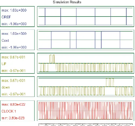
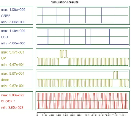
Figure 7 shows the simulation of the proposed structure as a phase-frequency detector to calculate the phase difference between the rising edges of two signals. In this figure, inputs are apply in such a way that all three possible states of inputs in two phase detectors are included: 1) CREF is ahead of COUT in rising edge, 2) CREF
and COUT are in phase, 3) CREF is lagged behind of COUT
in rising edge. As it can be seen, in the first rising edge, the CREF signal is two QCA clock cycles ahead of COUT,
and it is expected that UP also be logic one for two QCA clock cycles and DOWN signal does not exist. Also, in the second rising edge, these two signals are in phase, so none of UP and DOWN outputs will be activated. Finally, the CREF is three QCA clock cycles lagged behind COUT,
thus only the DOWN output signal is activated to the same extent. Therefore, this circuit performance can be verified by this simulation.
Figure 8 shows the simulation results of the proposed structure as a phase-frequency detector for calculating the phase difference between the rising edges of two signals with same frequency and constant phase difference, when the CREF is ahead of COUT. In this case,
UP is activated and due to the constant phase difference
of three QCA clock cycles, the UP pulses widths will be equal to three QCA clock cycles. Also, Figure 9 shows a condition that two signals have same frequency and CREF
is lagged from COUT by constant phase difference
(assuming that this phase difference is three cycles). Regarding the circuit operation, it is expected that DOWN is activated for three cycles in each period, which is confirmed by Figure 9.
Figure 10 shows a condition that two input signals have different frequencies. In this case, CREF is ahead of
COUT at some moments, and UP will be activated at the
same time. In other moments, COUT is ahead of CREF, and
DOWN would be activated as much as phase differences.
Figure 5. Proposed rising edge PFD
Figure 7. Simulation results of proposed rising edge PFD in three different cases
Figure 8. Simulation results of proposed rising edge PFD
when inputs have same frequency and CREF is ahead of COUT
Figure 10 confirms circuit performance in detecting the phase difference of inputs with different frequencies. For example, in first and second rising edges, CREF is
ahead of COUT for three and one clock cycles,
respectively, and corresponding output is generated at UP. In addition, in third and fourth rising edges, CREF is
lagged behind COUT for three and one QCA clock cycles,
and corresponding output is generated at DOWN.
Figure 9. Simulation results of proposed rising edge PFD
when inputs have same frequency and CREF is lagged from
COUT
Figure 10. Simulation results of proposed rising edge PFD
when two input signals have different frequencies
Figure 11 shows simulation of the proposed structure as a phase-frequency detector to calculate the phase difference between two signals falling edges. In this figure, the inputs are applied in such a way that all three possible conditions for two inputs of phase detector are included, 1) CREF is ahead of COUT in falling edge, 2) CREF
and COUT are in phase, 3) CREF is lagged behind of COUT
Figure 11. Simulation results of proposed falling edge PFD when inputs have same frequency and CREF is ahead of COUT
Figure 12. Simulation results of proposed falling edge PFD
when two input signals have different frequencies
edge, the CREF signal is three QCA clock cycles ahead of
COUT, and it is expected that output UP also be logic one
for three QCA clock cycles and DOWN signal does not exist. Also, in the second falling edge, these two signals are in phase, so none of the two UP and DOWN outputs will be activated. Finally, the CREF is three QCA clock
cycles lagged behind COUT in its falling edge, thus only
the output signal DOWN is activated to the same extent. Therefore, this circuit performance can be verified by this simulation. Figure 12 also shows a condition that input signals have different frequencies for detection of falling edges differences. In this case, at some moments CREF is
ahead of COUT and output UP is activated at the same
time. Also, in other moments COUT is ahead of CREF,
which DOWN would be activated during those moments. It should be mentioned that in this case, the phase differences of falling edges are being calculated.
In order to investigate the energy dissipation behavior of the proposed circuits, other simulations have been executed using QCAPro software [14]. Figure 13 and Figure 14 illustrate simulation results of the proposed structures that are sensitive to the rising and falling edges. In these figures, solid points represent points with more energy consumption. In addition, the energy dissipation parameters results are shown in Table 1.
Furthermore, with respect to the designed structures, the results obtained from simulations are presented in Table 2. According to this table, each of the proposed structure as a phase-frequency detector has 104 cells, 0.13 μm2 area and reset path delay of 1.5 QCA clock cycles. Another important point in these structures is that the inputs and outputs are available outside the circuit. It should be noted that due to the design of these PFDs in QCA technology, they have an ability to work in higher frequencies in comparison with CMOS circuits. In addition, in the table the average energy dissipation of the two proposed designs are compared.
TABLE 1. Energy dissipations of proposed PFDs
Average Switching Energy Dissipation(eV) Average Leakage
Energy dissipation(eV) Minimum Energy
Dissipation of circuit(eV) Maximum Energy
Dissipation among all cells(eV) Average Energy
Dissipation of circuit(eV) Maximum Energy
Dissipation of circuit(eV) Type
0.11371 0.04124
0.04106 0.00785
0.15495 0.27832
Rising Edge PFD
0.11302 0.04146
0.04073 0.00785
0.15448 0.27335
Falling Edge PFD
TABLE 2. Design characteristics of proposed PFDs
Type Number of Cells Area (µm2) Latency of Circuit Average Energy dissipation (eV)
Proposed Rising Edge PFD 104 0.13 1.5 cycle 0.27832
6. CONCLUSION
In this paper two new phase-frequency detector are
designed in quantum-dot cellular automata
nanotechnology. One of the designs is sensitive to rising edges and the other is sensitive to falling edge of input signals. Due to the design of these PFDs in QCA technology, they have an ability to work in higher frequencies in comparison with CMOS circuits. The proposed designs have the following advantages: small occupied area, few number of cells, good delay performance, and small reset path time. In addition, the inputs and outputs of the proposed design are available outside the circuit. This can help designer to easily connect them to other circuits.
7. ACKNOWLEDGMENT
This research work has been supported by a research grant from the University of Mazandaran.
2. REFERENCES
1. Gholami, M. and Zoka, S., "Two novel d-flip flops with level
triggered reset in quantum dot cellular automata technology",
International Journal of Engineering, Transactions C: Aspects,
Vol. 31, No. 3, (2018), 415-421.
2. Almatrood, A.F. and Singh, H., "Design of generalized pipeline
cellular array in quantum-dot cellular automata", IEEE
Computer Architecture Letters, Vol. 17, No. 1, (2017), 29-32.
3. Binaei, R. and Gholami, M., "Design of multiplexer-based d
flip-flop with set and reset ability in quantum dot cellular automata
nanotechnology", International Journal of Theoretical Physics,
Vol. 58, No. 3, (2019), 687-699.
4. Gholami, M., "Phase frequency detector using transmission gates
for high speed applications", International Journal of
Engineering, Transactions A: Basics, Vol. 29, No. 7, (2016),
916-920.
5. Ding, Z., Liu, H. and Li, Q., "Phase-error cancellation technique
for fast-lock phase-locked loop", IET Circuits, Devices &
Systems, Vol. 10, No. 5, (2016), 417-422.
6. Estebsari, M., Gholami, M. and Ghahramanpour, M.J., "A wide
frequency range delay line for fast-locking and low power
delay-locked-loops", Analog Integrated Circuits and Signal
Processing, Vol. 90, No. 2, (2017), 427-434.
7. Gholami, M., "Phase detector with minimal blind zone and reset
time for gsamples/s dlls", Circuits, Systems, and Signal
Processing, Vol. 36, No. 9, (2017), 3549-3563.
8. Gholami, M., "Total jitter of delay-locked loops due to four main
jitter sources", IEEE Transactions on Very Large Scale
Integration (VLSI) Systems, Vol. 24, No. 6, (2015), 2040-2049.
9. Batchu, S., Talari, J.P. and Nirlakalla, R., "Analysis of low power
and high speed phase frequency detectors for phase locked loop
design", Procedia Computer Science, Vol. 57, (2015),
1081-1087.
10. Liu, W., Swartzlander Jr, E.E. and O’Neill, M., "Design of semiconductor qca systems, Artech House, (2013).
11. Srivastava, S., "Probabilistic modeling of quantum-dot cellular automata", University of South Florida, 2008.
12. Compano, R., Molenkamp, L. and Paul, D., "Roadmap for nanoelectronics", European Commission IST programme, Future and Emerging Technologies, (2000).
13. Walus, K., Dysart, T.J., Jullien, G.A. and Budiman, R.A., "Qcadesigner: A rapid design and simulation tool for
quantum-dot cellular automata", IEEE Transactions on Nanotechnology,
Vol. 3, No. 1, (2004), 26-31.
M. Gholamia, R. Binaeib,M. Gholamnia Roshanb
a Faculty of Engineering and Technology, University of Mazandaran, Babolsar, Iran
b Department of Electrical and Computer Engineering, Mazandaran Institute of Technology, Babol, Iran
P A P E R I N F O
Paper history: Received 28 April 2019
Received in revised form 15 December 2019 Accepted 16 Januray 2020
Keywords: Quantum Cellular Automata Quantum-dot Cellular Automata Phase-frequency Detector Phase Detector Power Consumption کچ ی هد خا ی ار تعنص نورتکلا ی ک دشر گمشچ ی ر ی هتشاد تسا و ناققحم شلات م ی دننک هک خات ی ،ر حطس عطقم لاغشا ی و ناوت فرصم ی ار ات دح ناکما شهاک دنهد . رد ا ی ن ،اتسار ژولونکت ی اه ی ز ی دا ی فرعم ی هدش دنا . اتاموتا ی لولس ی موتناوک ی ( QCA ) ی ک ی زا ای ن ارب هک تسا اهشور ی حارط ی اهرادم ی قم ونان ی سا نورتکلا ی ک ی فرعم ی ا .تسا هدش ی ن ژولونکت ی اراد ی و لااب تعرس
م ناوت ص فر ی اپ یی ن هدوب و حطس فرصم ی مک ی دراد . هقلح لفق هدش خات ی ر ( DLL ) و هقلح لفق هدش زاف ( PLL ) هب روفو رد اهرادم ی تارباخم ی دروم هدافتسا رارق م ی گ ی دنر . ی ک ی رتمهم زا ی ن رد اهشخب DLL و PLL زاف زاسراکشآ ،اه
سناکرف
( PFD اربانب .تسا ) ی ن حارط ی ا ی ن ژولونکت رد رادم ی QCA مها ی ت ز ی دا ی ا رد .تشاد دهاوخ ی
ن زاف زاسراکشآ ود هلاقم
-ف دج سناکر ی د هبل هب ساسح اه
ی اپ یی ن ژولونکت رد هدنور لااب و ی
QCA فرعم ی حارط ود ره .دش دهاوخ ی زا 104 لولس کشت ی ل عطقم حطس و هدش
2 m μ 0.13 ار لاغشا هدرک دنا نچمه . ی ن خات ی ر ا ی ن اب ربارب اهرادم 5 / 1 س ی لک رد کلاک QCA حارط .تسا ی اه رد ی ک لا ی ه تروص هتفرگ تسا و مامت ی دورو ی اه و جورخ ی اه رد سرتسد دنتسه هک لباق ی ت هدافتسا رد تارادم د ی رگ ار دنراد . doi: 10.5829/ije.2020.33.02b.11