A Ring Oscillator Model and Design for a Self-biased
CMOS PLL using Alpha-Power Law Based MOSFETs
Bhaskar Gopalan
Email: [email protected]
Abstract – A simple modified design procedure for a Maneatis cell based ring oscillator without any elaborate bias generator suitable to self-biased CMOS PLL using alpha-power law based MOSFETs is presented. Also presented is the time-domain mathematical model for the simulation of voltage-controlled oscillator (VCO). The design shows how to fix the operating biasing current for VCO through a simple circuit. A closed-form solution for the model shows good agreement between the SPICE simulated design and the model. The VCO is simulated for a 0.13um, 1.2v process and the designed result shows the tuning range of the VCO vary from 190MHz to 540MHz. The maximum % Total harmonic distortion (%THD) obtained is 2% and the maximum power dissipated by the ring oscillator is 672μW. Also the maximum variation in oscillation frequency arising from low-frequency supply voltage noise is 7%. The proposed design also is compared with Maneatis cell based ring oscillator with bias generator and shown that proposed design without any elaborate bias generator is better in terms of supply voltage noise effect and %THD but poorer in terms of tuning range.
Keywords – Self-Biased CMOS PLL, VCO, SPICE Models, Alpha-Power Law Mosfets, VCO Tuning Range, Total Harmonic Distortion (THD), Power Dissipation And Supply Voltage Noise.
I.
I
NTRODUCTIONThe rising demand for high-speed I/O has created an increasingly noisy environment in which PLL’s must function. This noise, typically in the form of supply and substrate noise, tends to cause the output clock of PLL’s to jitter from their ideal timing. Achieving low jitter in PLL designs can be difficult due to a number of design tradeoffs. The amount of input tracking jitter produced as a result of supply and substrate noise is directly related to how quickly the PLL can correct the output frequency, To reduce the jitter, the loop bandwidth should be set as high as possible. Unfortunately, the loop bandwidth is affected by many process technology factors and is constrained to be well below the lowest operating frequency for stability.
This paper considers a Maneatis cell based VCO for the PLL [1] which is based upon self-biased techniques. Self-biasing can remove virtually all of the process technology and environmental variability that plagues PLL designs. Self-biasing can provide a bandwidth that tracks the operating frequency. Other benefits include a fixed damping factor for the PLL’s and input phase offset cancellation. Both the damping factor and the bandwidth to operating frequency ratio are determined completely by a ratio of capacitances giving effective process technology independence. By referencing most of all bias voltages and currents to other generated bias voltages and currents, the operating bias levels are essentially established by the operating frequency.
In this paper, a modified Maneatis VCO [1] without elaborate bias generator for the self-biased PLL using alpha-power law devices [2] is studied. A difference equation modeling of VCO is discussed in [3] and [6] whereas in this paper a mathematical modeling of VCO in closed-form expression has been obtained. A wide tuning range VCO is presented in [1] and [7]. The objective in this paper is to analyze and obtain a low-jitter VCO using alpha-power law devices against supply voltage noise and distortion.
This paper begins with a mathematical treatment for Maneatis cell based VCO model for a self-biased CMOS PLL in section II. Section III describes a simple modified design technique for Maneatis VCO. Also a supply voltage noise effect on VCO oscillation frequency is discussed in section III. Section IV concludes about the summary.
II.
A
M
ODEL FOR THEVCO
OF AS
ELF-B
IASEDPLL
Fig.1. Differential VCO delay stage with symmetric loads (Maneatis cell) - (Reproduced from Ref. [1]).
Fig.2 A three stage voltage controlled Ring Oscillator for the self-biased PLL [4].
Copyright © 2015 IJECCE, All right reserved diode-connected PMOS device in shunt with an equally
sized biased PMOS device. The buffer delay changes with Vm since the effective resistance of the load elements also
changes with Vm. These load elements lead to good
control over delay and high dynamic supply noise rejection. The simple NMOS current source is biased with Vbn.
Let the currents i1, i2, ic1 and ic2 be as shown in Fig.2.
Let x, y, z be the differential outputs of VCO for the three stages. 2Id is the biasing current for all the three cells. Let
the total linear capacitance at each output of the differential pair in the first stage be C and we can therefore write the equations at Vo+ and Vo- as follows. The
illustration below refers to the first cell and is well applicable for the other stages too.
o+ c2 2
o-c1 1
V
C
=i -i
t
V
C
=i -i
t
(1)Let Vo+ - Vo- = x, the differential output of the first stage
of the VCO. Let Kn and Kp be the transconductance parameters of NMOS differential pair transistors and symmetric load PMOS transistors respectively. Let vtn and vtp be the threshold voltages of NMOS and PMOS transistors respectively and α and αp be the alpha-power
values of NMOS and PMOS transistors respectively. From (1), we have for the first cell using [2],
2
1 c2 c1
x
C
=(i -i )+(i -i )
t
(2)Where,
c2 c1 1 d1 2 d2 m
i -i =- λ I +λ I
x+P x
(3)
αpd1 m
Kp
I =
V - vtp
2
(4)
αpd2 d m
Kp
I =I -
V - vtp
2
(5)
p p p 1 2/α α p p 2m d2 2/α
d2
d2
α -1 Kp
α
Kp
P
x =
2I
(-x) 1-
x
2
2I
4 2I
(6) and1 2 m n d
i -i
G (-z)-λ I x
(7)Where z = - (differential input voltage to the first cell). λ1
and λ2 are the channel length modulation parameters of top
PMOS transistors of symmetric load respectively. Id1 and
Id2 are the drain currents of these two transistors
respectively and λn is the channel length modulation
parameter of NMOS differential pair transistors.
1/α
1-1/α
2/α 2m d 2/α
d
α-1 Kn
α
G
z =
Kn
2I
z 1-
z
2
4(2I )
(8)
The biasing current 2Id varies with z for the first cell since 2
d o
2I =2I +mz
(9) Where 2Io is the input differential voltage independentbiasing current.
The value of m needed to cancel out the higher degree dependency of Gm (z) on z is given by [2],
o 2/α oα2I /8
m=
2I /Kn
(10)Assuming that the higher degree dependency of Gm (-z)
and Pm (x) have been cancelled out and assuming that,
1 d1 2 d2 o
λ I +λ I
λI
(11) Now, we have the equation (2) can be written as,
n
o m mx
C
+
λ+λ I +P x=- G z
t
(12)Similarly for the other two cells or stages, we have,
n
o m my
C
+
λ+λ I +P y=G x
t
(13)
n
o m mz
C
+
λ+λ I +P z=G y
t
(14)The equations (12), (13) and (14) constitute the model for the three cells of the VCO. In (12), (13) and (14), Gm
and Pm are given by (after neglecting higher order terms),
1/α
m o
o
α Kn
G =
2I
2 2I
(15)
1/α p m d2 d2α
Kp
P =
2I
2
2I
(16)Now let us assume that x, y, z are given by,
- t-tx0 /τ
- t-ty0 /τ
- t-tz0 /τ
x t
As+ A0-As e
y t
As+ A0-As e
z t
As+ A0-As e
(17)
Where As and A0 are steady-state and initial state values of the signals respectively and these are given for a rising exponential by As=A/2; A0=-A/2 and for a falling exponential by As=-A/2; A0=A/2, where (A/2) is the maximum amplitude of the signals x or y or z. The basic delay parameter τ using (12) is given by,
m n o
C
τ=
P + λ+λ
I
(18)Where Pm is given by (16) and C is the effective
capacitance at either output of the each VCO cell. Assuming that t = 0 and Substituting (17) in (12), (13) and (14), we obtain,
m
m m n o
2G
tz0=tx0=ty0=τ ln
G -P - λ+λ
I
(19)The frequency of oscillation is given by,
o
1
F =
From (17) and (12) we also obtain the maximum amplitude as given by,
os
ms 1 n os
I
A
=
2
P +P + λ+λ
I
(21)Where P1 is given by,
tx0 τ
1 ms n os
C
P =2
-P - λ+λ
I
e
τ
(22)WhereIos is the bias current at the point when the bias
current flows on only one of the two branches (i.e. i1 or i2
is zero / at the lower swing limit). Pms is obtained using
2Id2s in (16) where 2Id2s is given by
αpd2s os m
2I
=I -Kp V - vtp
(23)Having known all the parameter values in equation (17) and this completes the model for the VCO for a self-biased PLL based on alpha-power law devices.
III.
T
HEVCO
D
ESIGNFig.3. Modified VCO differential delay stage with PMOS transistor M8 in the biasing circuitry for biasing current
fixation.
The complete VCO delay stage circuit based on model discussed in the above section is shown in Fig.3. It doesn’t require any elaborate bias generator as in Ref. [1]. In Fig.3, Vm = vdd-Vbp. In the biasing circuitry, a NMOS
transistor (M7) is biased with Vbn and an only extra
element, a PMOS transistor (M8) is dynamically biased with Vbp as shown in Fig.3. A symmetrical PMOS
transistors form the loads for the VCO delay stage. Biasing current (2Io) =Current thro’ M7-Current thro’ M8.
The VCO cell delay changes with Vbp as the resistive
load changes. In the biasing circuit, the PMOS transistor (M8) is driven by Vm. This gives good control over
variation in the biasing current 2Id with Vbp and also gives
control over supply voltage noise. As the supply voltage increases or decreases slightly due to noise, the voltage at either outputs of delay stage increases or decreases and this changes the biasing current. This is approximately
compensated by PMOS transistor (M8) current in the biasing circuit driven by Vm. Also the low transistor sizes
of M1 and M2 make the higher degree dependency of Gm
on x or y or z to be minimized, thus making differential current an approximately a linear as shown in equation (10).
The various parameters chosen for the self-biased PLL are given below. Some of these parameters are taken from BSIM3v3.1 SPICE Models of 0.13um, 1.2v, IBM CMOS process and the device sizes are taken from the design of VCO.
Supply voltage, Vdd = 1.2v. epo = 8.8542e-12 F/m2.
Dielectric constant of oxide layer (erox) = 4.0. Oxide layer thickness (tox) = 4.1nm.
Vbn = 0.625v.
Kp = Kpp(Wp/Lp) = 13.85e-06*(0.6u/0.15u) A/Vα.
Kn = Knn(Wn/Ln) = 40.0e-06*(10.0u/0.15u) A/Vα.
vtn = 0.366v. vtp = -0.391v. λ = λn = 0.1/v.
α = 2.0.
αp = 1.05 or 2.0.
It is noted that at lower currents of Id2, the PMOS load
transistor has an alpha-power value of 2.0 whereas at moderately higher currents, it has an alpha-power value of 1.05. Also it is noted that Kp and αp in equation (23) show
different values as different from the above mentioned due to low currents and are given by,
Kp = Kpp(Wp/Lp) = 4.0e-06*(0.6u/0.15u) A/V α
. αp = 1.5 or 2.0.
The capacitance C is obtained from,
C1=(2.0/3.0)*(epo*erox/tox)*(WnLn+WpLp)=9.15f.
C = C1+Cgd,n+Cgd,p+2Cbd,p+Cbd,n = 15fF.
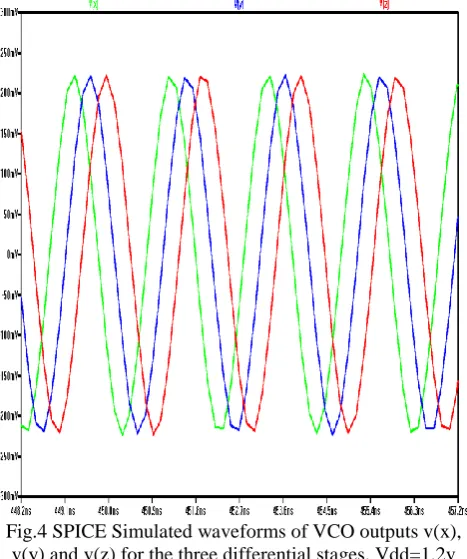
The SPICE simulated waveforms for the differential outputs of three differential stages for vdd=1.2v and Vbp=0.6v are shown in Fig.4. The VCO output frequency
in Fig.4 is 500MHz.
The various simulated and estimated parameters including frequency of oscillation for different Vbp are
tabulated in Table.I. The Table.I lists the values for VCO frequency obtained using SPICE simulated design and the model discussed in section II. It also shows that bias current 2Io is approximately a constant one.
The maximum amplitudes of the signals for different Vbp are tabulated in Table.II. This table shows the
amplitude of the signals obtained using SPICE simulated design and the proposed model as described in section II. A simple level-shifter may be used at the outputs of VCO to convert the differential signals into single-ended rail-rail voltages.
The changes in the frequency of oscillation and the maximum amplitude of the signals between SPICE simulation and the proposed model (as noticed in Table.I and II) are due to the variations in the device parameters namely KPn, KPp, vtn, vtp, α, αp, λn and λ with respect to
Copyright © 2015 IJECCE, All right reserved Table.III shows %Total harmonic distortion (%THD)
and the power dissipated by VCO (in μW) for different control voltage. The power dissipation varies with respect to Vbp due to the presence of transistor (M8) in delay stage
circuit as in Fig.3.
The variation in VCO frequency for a low-frequency square wave supply voltage noise is also studied. The amplitude of the noise is chosen as +/-2.5% of vdd. For vdd=1.23v and Vbp=0.6v, the SPICE simulated values are
2Io=37uA and Fo=535MHz (a change of 7%). Similarly for
vdd=1.17v and Vbp=0.6v, the SPICE simulated values are
2Io=25uA and Fo=465MHz (a change of 7%).
It is simulated and studied that the effect of supply voltage noise is more in Maneatis cell based VCO (with elaborate bias generator as in Ref. [1]) than the present proposed design and the change in oscillation frequency for a typical case is more than 10% in the former case. Also the %THD is approximately twice in Maneatis VCO with bias generator than the proposed design. But the tuning range is much larger in the former case (583MHz) than the proposed design (350MHz).
Fig.4 SPICE Simulated waveforms of VCO outputs v(x), v(y) and v(z) for the three differential stages. Vdd=1.2v and Vbp=0.60v. The VCO output frequency is 500MHz.
Table I: The VCO Frequency Results Vbp
volts)
2Io
(uA)
2Id2
(uA)
VCO Fo (MHz)
Design (Simulated)
Model (SectionII)
0.45 24.0 2.90 194.2 222.0
0.50 32.0 12.93 365.1 415.4
0.55 33.0 16.60 453.3 459.0
0.60 34.0 20.20 499.0 497.0
0.65 27.5 23.60 522.7 534.4
0.70 28.0 24.80 533.6 536.8
0.75 28.4 25.60 538.5 538.6
0.80 28.7 26.10 538.6 539.9
Table II: The Results of Maximum Amplitude of signals
Vbp
(volts) 2Io
(uA) Ios
(uA)
Maximum Amplitude, A/2 (in mv)
Design (Simulated)
Model (Section II) 0.45 24.0 12.0 607 578 0.50 32.0 20.0 366 316 0.55 33.0 20.66 282 259 0.60 34.0 20.70 220 220 0.65 27.5 20.75 180 166 0.70 28.0 20.73 160 165 0.75 28.4 20.19 152 159 0.80 28.7 20.53 148 162
Table III: Simulated Results of % Total harmonic distortion and Power dissipation. Vbp
(volts)
Fo
(MHz) (Simulated)
%THD (Simulated)
Power Dissipation in μW (Simulated) 0.45 194.2 1.84 672 0.50 365.1 1.67 500 0.55 453.3 2.06 328 0.60 499.0 1.59 205 0.65 522.7 1.64 138 0.70 533.6 2.07 109 0.75 538.5 1.51 99 0.80 538.6 1.93 95
IV.
C
ONCLUSIONA simple modified design of Maneatis cell based Ring
oscillator without any elaborate bias generator suitable to a self-biased CMOS PLL using alpha-power law devices was discussed. The design includes fixing of the biasing current corresponding to variation in the control voltage. Also an approximate mathematical model for the same ring oscillator has been presented. The designed SPICE results show close agreement between the SPICE and the model results. The results of oscillation frequency, amplitude of the signals, power dissipation and the %Total harmonic distortion were studied. The variation in oscillation frequency due to low-frequency supply voltage noise was also studied and the results were given. Also the results for the Maneatis cell based ring oscillator with bias generator and the proposed modified design were compared.
R
EFERENCES[1] John G. Maneatis , “Low-Jitter Process-Independent DLL and
PLL Based on Self-Biased Techniques”, IEEE J. of Solid-State Circuits, vol.31, No.11, pp.1723-1732, Nov.1996.
[2] Bhaskar Gopalan, “Design of Linear CMOS Transconductance
Elements for Alpha-Power Law based MOSFETs and an Automatic Compensation Technique for Temperature”, Universal Journal of Electrical and Electronic Engineering, Horizon Research Publishing, USA, Vol.2, no.5, pp.234-244, 2014.
[3] David Johns and Ken Martin, “Analog Integrated Circuit
[4] Behzad Razavi, “Design of Analog CMOS Integrated Circuits”, McGraw Hill, Inc., 2001.
[5] R.Best, Phase-locked loops, McGraw-Hill,1993.
[6] Monolithic Phase-Locked Loops and Clock Recovery Circuits:
Theory and Design, Edited by Behzad Razavi, IEEE Press, 1996.
[7] I. Young et.1l., “A PLL clock generator with 5 to 110MHz of
lock range for microprocessors”, IEEE J.Solid State Circuits, vol.27, no.11, pp.1599-1607, Nov.1992.