This is an open access journal, and articles are distributed under the terms of the Creative Commons Attribution-Non Commercial-ShareAlike 4.0 License, which allows others to remix, tweak, and build upon the work non-commercially, as long as appropriate credit is given and the new creations are licensed under the identical terms.
© 2018 Journal of Advanced Pharmacy Education & Research | Published by SPER Publication
25
Structural, Optical and Humidity Sensitivity for CdSe
Nanocrystalline Thin films
Hussein Hakim Abed
1*, Hayder M. Abduljalil
1, Mudar Ahmed Abdulsattar
21Department of Physics, College of Science,University of Babylon, Iraq, 2Ministry of Science and Technology, Baghdad, Iraq.
Correspondence:Hussein Hakim Abed, University of Babylon, College of Science, Department of Physics, Iraq, E-mail: [email protected]
ABSTRACT
The CdSe nanocrystalline thin films were fabricated on different substrates (silicon, indium tin oxide and glass) with different thicknesses (225, 250, and 300) nm by the pulsed laser deposition (PLD) technique. These thin films were characterized by the structural and optical measurements. From the X-ray diffraction (XRD), it was found that the thin films had hexagonal wurtzite structure. Crystallite size of the thin films increased from 13.56 nm to 21.368 nm with the increased thickness from 225nm to 300 nm. The atomic force microscopy images showed that the surface topography of the thin films got more homogeneity with the increased thickness. Optical properties have been performed by investigating the transmittance spectra in the spectral region (300–700) nm, and it was found that the thin films had the transmittance which increased with the increased wavelengths in the visible region, and the edge energy gap shifted from 1.8 eV to1.7 eV with the increased thickness from 225 nm to 300 nm, making the thin films suitable to be used in the optoelectronic and solar cell applications. The resistance of thin films was changed with the relative humidity, and their sensitivity was increased with the increased grain size and thickness, making CdSe thin films suitable to be used as a humidity sensor.
Keywords:CdSe; Nanocrystalline; Humidity Sensor.
Introduction
Nanoparticulate materials have engrossed increasing responsiveness in the last decades. For this, the unique combination of the small size, interesting properties, and good processability, have been opening the flexibility of their use in many technical and biomedical applications [1].
II-VI compound semiconductors have the band gap between 1-3 eV in the visible region, therefore their assistance in optoelectronic devices has been notable [2]. Cadmium selenide
(CdSe) is one from this group. Three crystalline forms of CdSe have been known: wurtzite (hexagonal), sphalerite (cubic) and rock-salt (cubic) [3]. CdSe quantum dots have been used for laser
diodes, nanosensing, and biomedical imaging [4].
Wurtzite structures for CdSe are more stable than zincblende structures [5]. However, CdSe quantum dots characteristic is
dependent on the size of the crystal. This makes them an excessive material for use in chemical and biological sensors P[6]P.
Smaller dots make the optical absorption and emission of quantum dots move to the blue region [7]. Humidity is a very
significant and important factor. Its measurement and regulation is vital for diverse productions and human security [8, 9]. Many reports of humidity sensors have been built on polymer
composites and porous ceramics [10, 11]. Electronic humidity
sensors have been used in certain serious locations, remote places, potentially explosive atmospheres and areas with extraordinary electromagnetic interfering which is either difficult or occasionally unmanageable [12]. Electronic humidity
sensors are available at low-cost today. Most of these sensors can be linked to a microprocessor without needing a peripheral amplifier or digitizer.
In latest years, in order to develop the device and also to invent new applications, main concentration has been given to the study of the electrical and optical properties of CdSe thin films. CdSe are very sensitive to the manufacturing procedure used. Therefore, the study of the properties of CdSe with respect to different conditions is a matter of high significance. CdSe thin film has been prepared using a variation of methods with sputtering, spray pyrolysis, and electrodepositing.
Pulsed Laser Deposition (PLD) is a very appropriate method for gaining uniform film under different deposition parameters and
Access this article online
Website: www.japer.in E-ISSN: 2249-3379
How to cite this article: Hussein Hakim Abed, Hayder M. Abduljalil, Mudar Ahmed Abdulsattar. Structural, Optical and Humidity Sensitivity for CdSe Nanocrystalline Thin films. J Adv Pharm Edu Res 2018;8(4): 52 -31.
changing thickness by controlling the number of pulses. In view of this, an effort has been made to study the structural and optical properties of CdSe thin films prepared by (PLD) and their application as a humidity sensor.
Experimental Technique
The CdSe thin films of different thickness (225, 250 and 300) nm were deposited on a different substrate (silicon, indium tin oxide and glass) by nano pulse Nd: YAG laser (λ=1064 nm, repetition rate of 6 Hz and the pulse duration is 10 ns) through using the pulsed laser deposition technique. The pressure was saved below 10-5 Torr. The CdSe (disk form radius 1cm and
thickness 2mm) was targeted by a laser beam emitted from Nd: YAG laser. The evaporated particles were deposited on substrate as a thin film. The energy of laser beam gun was 80 mJ during the deposition of thin films. The substrate was placed at a distance of 3.5 cm from the source materials. Through deposition of the thin film, the substrate was placed normally to the line of sight from the evaporation surface at different polar angles to obtain uniform deposition.
The substrate temperature was measured using digital temperature attached to a thermocouple sensor. The temperature of the substrate was (523 K). The thin films were annealed at (573 K) for (2 hours). The thickness of the thin films was measured using optical thin film measurement (LIMF-10). The structural properties of thin films with silicon substrate were studied by using X-ray diffraction forms recorded by D-8, Discover XRD-diffractometer (Bruker) using CuKα1 radiation (λ=1.54Å) with Ni-filter. The topography of the surface of thin films with indium tin oxide substrate was determined by atomic force microscopic (AFM), and the optical band gap of the CdSe thin films was recorded by using double beam UV-Vis spectrophotometer in the wave length range of (300-700) nm. Silver electrodes were precipitated on the surface of the samples with glass substrate by using DC sputtering (with width 0.2 cm and distance 0.1 cm between them). The samples were placed in a container, and the water vapor was used as a source of humidity. The regulator network monitored and measured variations in humidity. The electrical resistance to different humidity range of (40%–80%) was measured by using the Keithley electrometer type 2400 source meter.
Results and Discussion
Structure Properties
The CdSe thin films were characterized by the analysis of X-ray diffraction (XRD) patterns. The measured XRD patterns at a diffraction angle (2θ) from 20 to 27degree for these thin films have been shown in Fig. 1. The XRD patterns revealed that the films were polycrystalline because these had more than one peak. The peaks (002) and (100) were corresponding to a hexagonal structure. The intensity of (002) peak increased with
the increased thickness. The experimental d-values for high peak and ASTM d value (3.505 Å) were in good agreement and indicated the creation of a hexagonal (wurtzite) structure. The special orientation of CdSe was found to be mainly along (002) plane and the direction of orientation was in c-direction. The intensity (002) peak was observed in all thin films which indicated that (002) plane had a favorable orientation. Similar structures and preferred orientations have also been reported by other investigators [2, 13, 14]. The intensity of (002) peaks was
increased with the rise of the thickness due to the enhancement in crystallinity of the thin films. The lattice constants (a and c) of CdSe thin films were calculated by the following equation [14]
as given in Table 1.
1
𝑑𝑑2= (4(h
2+ℎk2+k2) 3𝑎𝑎2 ) +𝑐𝑐𝑙𝑙2
2
(1)
Where d is inter-planar spacing and (h k l) is Miller indices. The full-width at half maxima (FWHM) β and crystallite size D was evaluated, as given in Table 1. The crystallite size of the thin films was calculated by the equation [15]:
D = 0.94∗ �βCOSθλ � (2)
Where λ is the wavelength of X-ray (1.54 Å) and θ is a diffraction angle.
It was observed from XRD patterns that β corresponding to (002) plane decreased with the increase of thickness from 225 to 300 nm due to the improvement of crystallinity in the thin films. It was observed from Table 1 that the crystallite size of the thin films increased by increasing their thickness. The observed lattice constants were in agreement with the results reported by the other researchers [13, 14] with the standard value
of [08-0459JCPDS].
0 10 20 30 40 50
20 21 22 23 24 25 26 27
Thickness 225 nm
(
100)
(
002)
2θdegree
In
te
ns
0 10 20 30 40 50
20 21 22 23 24 25 26 27
Thickness 250 nm
Int
ens
ity
(100) (002)
2θdegree
0 20 40 60
20 21 22 23 24 25 26 27
Thickness 300 nm
2θdegree
Int
ens
ity
(100)
(002)
Figure 1: XRD patterns of CdSe thin films.
Table 1: X-ray diffraction parameters for CdSe thin films. Thickness
(nm) (hkl) (deg) 2Ө (nm) d (nm) D
Lattices constant a (Å)
Lattices constant c (Å) 225 (002) 25.4 3.5 13.56 4.05 7.01
)
100
( 23.536 3. 71
250 ((0100)02) 25.365 3.5085 23.92 3.722 20.452 4.29 7.02
300 (002)(100) 25.438 3.498 24.16 3.685 21.368 4.25 7
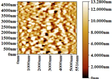
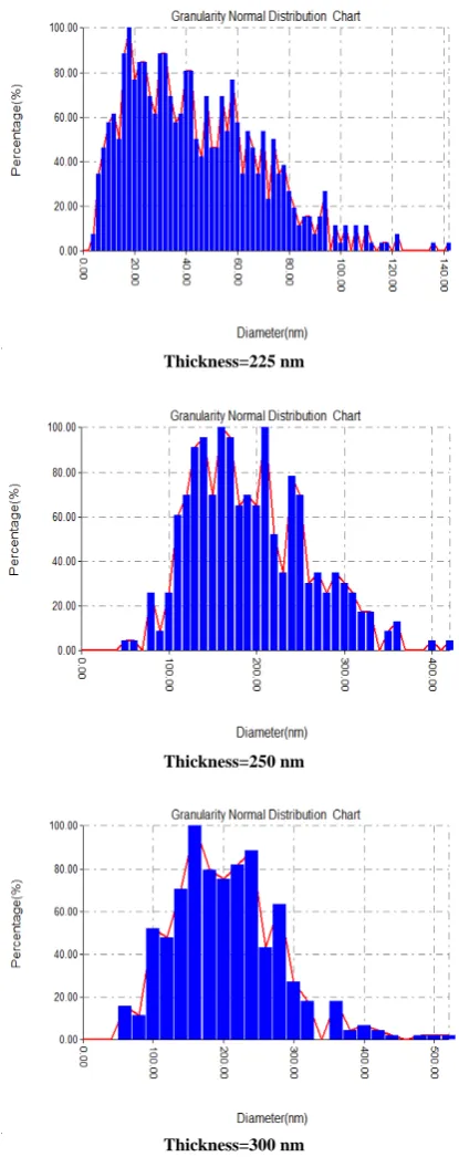
Fig. 2 and Fig. 3 show the surface topography of the thin films, as depicted by the AFM images, indicating that the distribution of grains became more uniform with the increase of the thickness. Fig. 4 shows the histograms of the growth of granular groups on the surfaces of the deposited thin films. The regularity increased with the increased thickness of the prepared thin films may be because the time of the deposited thin films increased with the increased thickness. Long time gives higher susceptibility to the atoms to rearrange themselves on the hot surface and fill the holes on the surface so that the surface becomes more regular.
Thickness=225 nm
Thickness=250 nm
Thickness=300 nm
Figure 2: Shows the 2dimensions AFM image of CdSe thin films.
Thickness=225 nm
Thickness=300 nm
Figure 3: Shows the 3dimensions AFM image of CdSe thin films.
Thickness=225 nm
Thickness=250 nm
Thickness=300 nm
Figure 4: Shows the histograms of CdSe thin films.
As shown in Table 2, the root mean square of the surface roughness decreased with the increased thickness proving that the grains were uniformly distributed with the sensing area as used for the approximation of the grain size on the thin film surface, this surface characterization has been important for the applications such as humidity sensors, gas sensors and catalysis
[16].
Table 2: AFM images characteristics of the CdSe thin films.
Thickness of
CdSe thin films Average (nm) Roughness Square (nm) Root Mean Average Grain Size (nm)
225 2.75 3.33 42.64
250 1.88 2.51 188.81
300 1.42 1.84 194.73
The roughness rate and the root mean square of CdSe thin film for 300 nm were the smallest among the other thin films. It was obvious that the surface was smooth, and the decrease of the root mean square in CdSe thin film led to the increasing crystalline growth in the vertical direction more than the horizontal direction. Also, the increase of the grain size by increasing the thickness could be observed, this led to the surface homogeneity, and this result agreed with XRD results.
Optical Properties
The transmission of thin films depended on the wavelength of the incident photon, chemical composition, thickness, crystal structure and thin films surface morphology. The transmittance spectra of the CdSe thin films detailed in the wavelength from 300 to 700 nm were compared as a function of thickness as shown in Fig. 5. As Fig. 5 indicates, the thin films transmittance increased with the increase of the wavelength and decreased with the increase in thicknes. The thin film (300 nm) had a low transmittance in visible regions because of having the large grain size. The transmittance decreased with the increase of the grain size of CdSe thin films. The thin films which have a high transmittance in the visible region, and low transmittance in ultraviolet region, can be applied in optoelectronics and solar cells [17, 18].
Figure 5: Shows the transmittance of CdSe thin film versus wavelength.
The absorption coefficient α was evaluated by using the following relation [15, 19].
0 0.1 0.2 0.3 0.4 0.5 0.6 0.7 0.8 0.91
300 400 500 600 700
225 nm 250 nm 300 nm
Wavelength (nm)
Tr
an
ss
ma
ta
α=2.303At (3)
Where A is the absorbance and t is the thickness of thin films. The absorption coefficient is a function of the photon energy with different thicknesses as shown in Fig.6. It is clear from this figure that the absorption edge shifted to the lower energy with the increased thickness.
Figure 6: Shows the absorption coefficient as a function for photon energy.
The optical band gap of the thin films was calculated by using Tauc's equation [20].
αhυ= B(hυ −Eg)
1
n (4)
Where: hυ is photon energy and B is constant. n =1/2 for the direct transition.
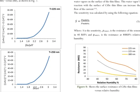
To calculate the direct optical band gap, in this study, plot (αhυ) 2 versus (hυ), as shown in Fig. 7.
Figure 7: Shows the (αhυ)2 versus (hυ) for thin films with
different thickness.
As can be seen in Fig.7, the edge energy gap of the thin film 225 nm was greater than the others, and it shifted from 1.8 eV to 1.7 eV with increasing the thickness from 225 nm to 300 nm. The thin film 225nm had a smaller grain size, therefore a quantum confinement caused the shift in the edge energy gab to the higher energy with decreasing the grain size [21].
Humidity Sensors
Variations in the electrical characteristics of the thin films with humidity have made them suitable to be used as humidity sensors. The structure and thickness of the thin films have been important to develop the performance of the sensors [19].
Porosity in thin films has produced the adsorption sites increasing the sensitivity of the sensor [20].
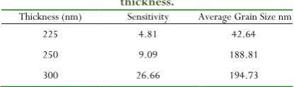
Fig. 8 shows resistance as a function of the relative humidity of the thin films for CdSe nanoparticles. The resistance decreased with increasing the humidity because of the adsorption of the water vapors on the surface of the thin films. This water vapor’s reaction with the surface of CdSe thin films can increase the flow of the current [21].
The sensitivity was calculated by using the following equation:
𝑆𝑆=𝜌𝜌80𝑅𝑅𝑅𝑅%
𝜌𝜌40𝑅𝑅𝑅𝑅% (5)
Where: S is the sensitivity, 𝜌𝜌R40RH% is the resistance of the sensor
in 40 RH% and ρ80RH% is the resistance at 80RH% relative
humidity.
Figure 8: Shows the surface resistance of CdSe thin films versus relative humidity
0 5000 10000 15000 20000 25000 30000
1 1.5 2 2.5 3 3.5
225 nm 250 nm 300 nm
photon energy (𝑒𝑒𝑉𝑉)
ab so rp tio n coe ffi cie nt (cm -1) 0 1E+09 2E+09 3E+09 4E+09 5E+09 6E+09
1 1.4 1.8 2.2 2.6 3 3.4
T=225 nm 〖 ( 𝛼𝛼ℎ 𝜐𝜐 ) 〗 ^2 〖𝑐𝑐 𝑚𝑚 〗 ^( − 2) 〖𝑒𝑒 𝑉𝑉〗 ^2 (ℎ𝜐𝜐)𝑒𝑒𝑉𝑉 0 1E+09 2E+09 3E+09 4E+09 5E+09 6E+09 7E+09 8E+09
1 1.4 1.8 2.2 2.6 3 3.4
T=250 nm 〖 ( 𝛼𝛼ℎ 𝜐𝜐 ) 〗 ^2 〖𝑐𝑐 𝑚𝑚 〗 ^( − 2) 〖𝑒𝑒 𝑉𝑉〗 ^2 (ℎ𝜐𝜐)𝑒𝑒𝑉𝑉 0 1E+09 2E+09 3E+09 4E+09 5E+09 6E+09 7E+09 8E+09 9E+09
1 1.4 1.8 2.2 2.6 3 3.4
T=300 nm 〖 ( 𝛼𝛼ℎ 𝜐𝜐 ) 〗 ^2 〖𝑐𝑐 𝑚𝑚 〗 ^( − 2) 〖𝑒𝑒 𝑉𝑉〗 ^2 (ℎ𝜐𝜐)𝑒𝑒𝑉𝑉 0 10 20 30 40 50 60 70 80 90
30 40 50 60 70 80
225 nm 225 nm 300 nm Re sist an ce ( M Ω )
Water adsorption increased with the increase of the grain size, so that the sensitivity increased as shown in Table 3 [22].
As shown in Fig. 9, the thin film with the thickness of 300 nm exhibited significantly the highest sensitivity because of the high surface area that facilitated the reaction with water vapor. For humidity sensor application, better sensitivity meant a highly active surface [23, 24].
Figure 9: Shows the sensitivity of CdSe thin films versus thickness.
Table 3: Shows sensitivity of CdSe thin films versus thickness.
Thickness (nm) Sensitivity Average Grain Size nm
225 4.81 42.64
250 9.09 188.81
300 26.66 194.73
Conclusion
CdSe thin films have been prepared by pulse laser deposition at different thicknesses having a hexagonal structure (wurtzite) and the favored direction along (002) plane. The increasing thickness increased the crystallite size. AFM images showed that the surface topography became smooth and homogenous with the increase of the thickness. The transmittance of the thin films in visible regions decreased with the increase of the thickness, and the edge energy gap shifted from1.8 eV to1.7eV making the thin films suitable for the optoelectronic and photo electronic applications. CdSe thin films have a sensing property for the humidity. The thin film with the thickness of (300 nm) had a high sensitivity comparing to the other thin films.
References
1. K.h.j. Buschow, "hand book of magnetic materials”, volume 16, (2000).
2. D. Patidar, K. S. Rathore, N. S. Saxena, Kananbala Sharma, and T. P. Sharma, "Energy band gab and conductivity measurement of CdSe thin film", Chalcogenide Letters Vol. 5, No. 2, February, p. 21– 25(2008).
3. Lev Isaakovich Berger, "Semiconductor materials", CRC Press p. 202. ISBN 0-8493-8912-7 (1996).
4. Christopher Ma, Yong Ding, Daniel Moore, Xudong Wang, and Zhong Lin Wang,"Single-Crystal CdSe Nanosaws”, J. AM. CHEM. SOC. 9 Vol. 126, No. 3709, (2004).
5. M. A. Abdulsattar, "Molecular approach to hexagonal and cubic diamond nanocrystals", Carbon lett., 16 192-197(2015).
6. Elizabeth M. Boatman and George C. Lisensky Karen J. Nordell,"A Safer, Easier, and Faster Synthesis for CdSe Quantum Dot Nanocrystals", Vol. 82 No. 11 November • Journal of Chemical Education (2005), pp. 1150-1156. 7. B. O. Dabbousi, J. Rodriguez-Viejo, F. V. Mikulec, J. R.
Heine, H. Mattoussi, R. Ober, K. F. Jensen, and M. G. Bawendi,"(CdSe)ZnS Core-Shell Quantum Dots”, Synthesis and Characterization of a Size Series of Highly Luminescent Nanocrystallites" J. Phys. Chem. B, 101, 9463-9475(1997).
8. Yamazoe, N.; Shimizu, Y.,"Humidity sensors: Principles and applications", Sens. Actuators 1986, 10, 379–398. 9. Irani F.S., Tunaboylu B. Saw humidity sensor sensitivity
enhancement via electrospraying of silver nanowires. Sensors. 2016; 16:2024 doi: 10.3390/s16122024. 10. Li, H.; Zhang, J.; Tao, B.; Wan, L.; Gong,
W.,"Investigation of capacitive humidity sensing behavior of silicon nanowires", Phys. E Low-Dimens. Syst. Nanostruct. 41, 600–604. (2009).
11. I. R. Agool, K. J. Kadhim and A. Hashim, "Fabrication of new nanocomposites: (PVA-PEG-PVP) blend-zirconium oxide nanoparticles for humiditysensors", Int. J. Plast Technol 21:397-403(2017).
12. S. A. Kolpakov, N. T. Gordon, C. Mou and K. Zhou,"Toward a New Generation of Photonic Humidity Sensors", Sensors 2014, 14, 3986-4013; doi:10.3390/s140303986
13. S. R. Vishwakarma, A. Kumar, S. Prasada and R. S. N. Tripathi, "Synthesis and characterization of n-CdSe thin films deposited at different substrate temperature " Chalcogenide Letters, Vol. 10, No. 10, p. 393 – 402 October (2013).
14. T.C.M. Santhosh, Kasturi V. Bangera and G.K. Shivakumar "Synthesis and band gap tuning in CdSe(1-x) Te(x) thin films for solar cell applications", Solar Energy 153, 343–347, (2017).
15. Z. M.S.H. Khan, S. A. Khan, M. Zulfequar, "Study of thiol capped CdSe quantum dots using SeO2 precursor for selenium source", Mater. Sci. Semicond. Process. 57 190–196, (2017).
16. I. Khan, I. Ahmad, H.A. R. Aliabad, S. J. Asadabadi, Z. Ali, M. Maqbool, "Conversion of optically isotropic to anisotropic CdSxSe1-x (0≤x≤1) alloy with S concentration", Comput. Mater. Sci, 77, 145–152, (2013).
17. A. Abbassi, Z. Zarhri, Ch. Azahaf, H. Ez‑Zahraouy and A. Benyoussef,"Boltzmann equations and ab initio calculations: comparative study of cubic and wurtzite CdSe", SpringerPlus 4:543(2015).
0 5 10 15 20 25 30
100 150 200 250 300 350
Thickness nm
Se
nsit
iv
18. E. Albrasi "Characteristics of CdSe Nanocrystalline Thin Films at Two Immiscible Liquids "American Scientific Research Journal for Engineering, Technology, and Sciences (ASRJETS) Vol. 27, No 1, 116-121, (2017). 19. H. H. Abed,"Study the Optical Properties of
(PVA-PEG-CoO) Nanocomposites", Australian Journal of Basic and Applied Sciences, 8(17), 591-594 November (2014). 20. P. J. Tauc,"Amorphous and Liquid Semiconductors",
New York (1974).
21. Z. Guo and L. Tan, "Fundamentals and Applications of Nanomaterials", Artech House (2009).
22. Zhu, Y., Yuan, H., Xu, J., Xu, P., Pan," Q. Highly stable and sensitive humidity sensors based on quartz crystal
microbalance coated with hexagonal lamelliform monodisperse mesoporous silica SBA-15 thin film", Sens. Actuators B Chem. 144, 164–169 (2010).
23. Kim, H., Sathaye, S.D., Hwang, Y.K., Jhung, S.H., Hwang, J., Kwon, S.H., Park and S., Chang, J.," Humidity sensing properties of nanoporous TiO2–SnO2 ceramic sensors", Bull. Korean Chem. Soc. 26(11), pp. 1881-1884, (2005).