c
Sharif University of Technology, June 2010
Structural and Magnetic Study of Active
Screen Plasma Nitrided Fe
73:5
Si
13:5
B
9
Nb
3
Cu
1
and Fe
77
Si
11
B
9
Nb
2:4
Cu
0:6
Ribbons
E. Memarzadeh Lotfabad
1, H.R. Madaah Hosseini
1;,
H. Asghari Shivaee
2and S. Roostaie
3Abstract. The comparative study of Active Screen Plasma Nitriding (ASPN) treatment of two Finemet-type alloys with the compositions of Fe73:5Si13:5B9Nb3Cu1 and Fe77Si11B9Nb2:4Cu0:6 was
investigated in dierent temperatures ranging from 410C to 560C. Dierential Scanning Calorimetry
(DSC), X-Ray Diractometery (XRD), Atomic Force Microscopy (AFM), Scanning Electron Microscopy (SEM), electrical resistivity, microhardness measurements and magnetic characterization by a Vibrating Sample Magnetometer (VSM) were utilized to characterize the treated samples. The comparison of the DSC data for the alloys suggested that the smaller amount of Nb as a growth inhibitor shifted the crystallization temperatures towards lower temperatures. Thus, the crystalline volume fraction and grain size in each temperature for Fe77Si11B9Nb2:4Cu0:6alloy increased compared to Fe73:5Si13:5B9Nb3Cu1alloy.
The size of iron nitrides on the surface of the ribbons with the lower Si content was larger. The electrical resistivity for the annealed and nitrided Fe77Si11B9Nb2:4Cu0:6 alloy was lower compared to the annealed
and nitrided Fe73:5Si13:5B9Nb3Cu1alloy, due to the larger grain size and lower Si content of Fe(Si) phase
in Fe77Si11B9Nb2:4Cu0:6 alloy. The VSM results showed that the maximum saturation magnetization and
coercivity at 440C were obtained in Fe
77Si11B9Nb2:4Cu0:6 alloy after nitriding under 75% H2 and 75%
N2 gas mixture, respectively.
Keywords: Fe-Si-Nb-B-Cu alloys; Comparative study; Crystallization; Active screen plasma nitriding.
INTRODUCTION
The Fe-Cu-Nb-Si-B nemet alloys exhibit excellent soft magnetic properties due to nanocrystalline -Fe(Si) grains dispersed in a residual amorphous matrix [1,2]. These alloys are derived from the conventional Fe-Si-B system with minor additions of copper (Cu) and niobium (Nb). In this case, Cu acts as nucle-ating agent, whereas Nb inhibits the grain growth of the FeSi phase that crystallizes from the amor-phous matrix during annealing. The Finemet alloys
1. Department of Materials Science and Engineering, Sharif University of Technology, Tehran, P.O. Box 11155-9466, Iran.
2. Institute for Nanoscience and Nanotechnology, Sharif Uni-versity of Technology, Tehran, P.O. Box 14588-89694, Iran. 3. Department of Mining and Metallurgical Engineering, Amir
Kabir University of Technology, P.O. Box 15875-4413, Tehran, Iran.
*. Corresponding author. Email: [email protected]
Received 16 February 2010; received in revised form 13 April 2010; accepted 21 August 2010
are prepared by the melt-spinning technique followed by annealing at elevated temperatures to achieve a nanocrystalline structure [2,3]. Their magnetic prop-erties depend on chemical compositions and also are able to be optimized by applying a heat treatment in temperature ranges close to the crystallization temperature [4]. Koster and Meinhardt [5] studied primary crystallization of Finemet alloys and found that the growth of nanocrystals can be controlled by selecting proper composition. Changes in the type or content of elements in Finemet alloys are known to be one way to improve magnetic, corrosion and mechanical properties [6,7]. The method and condition of nanocrystallization treatment have also important role in the formation of the nanocrystalline state [8]. Although classical thermal treatments under vacuum are used commonly, thermo-chemical treatments which are used in the steel industry also can be applied. These treatments act by thermal diusion of one or more external elements. In nitriding thermo-chemical treatment, the element used is nitrogen which results
in the improvement of some mechanical properties. The diusion of nitrogen atoms and chemical surface modications produce structural modications leading to substantial improvements in the properties of the material [8,9]. Gas Nitriding (GN) treatment gives a slightly improved nanocrystalline state by decreasing the -Fe(Si) grain size and increasing the crystalline volume fraction in Finemet ribbons which results in decreasing the magnetostriction. However, using the higher parameters of crystallization (520C and 6 h)
than those commonly used in the conventional treat-ment (500C and 1 h) results in signicantly higher
coercivity for the gas nitrided samples [8].
Plasma nitriding process is widely used and has a number of distinct advantages over the gas nitriding treatment, for example the non-emission of pollutants, energy economy and lesser treatment time [10]. Fur-thermore, it can be applied in lower temperatures due to plasma activation. After nitriding, a thin compound layer is produced on the component surface and a nitrogen diusion layer is formed beneath it. The extent of surface hardness increasing depends on the process parameters, such as temperature, atmosphere and the alloying elements in substrate. In common plasma nitriding, the components are heated as a result of ion bombardment on the surface. The components with dierent shape or dierent ratio of surface to mass may undergo dierent ion bombardment intensity. As a result, the inhomogeneous temperature distribution occurs on dierent components or dierent parts and hardness and depth of nitrogen diusion after plasma nitriding are inhomogeneous [11]. In order to reduce the eect of the above-mentioned disadvantages, some new processes were developed. Recently, a method named \Active Screen Plasma Nitriding" (ASPN) is introduced in which the specimens are placed inside a cylindrical steel screen on which cathodic potential is applied, leading to formation of plasma on the screen not on the specimens, and the required heat for the process is supplied from the screen radiation [11-13].
The aim of this study is to compare the struc-tural, mechanical, electrical and magnetic properties of two types of crystallized Finemet amorphous ribbons with the compositions of Fe73:5Si13:5B9Nb3Cu1 and
Fe77Si11B9Nb2:4Cu0:6submitted to ASPN and
conven-tional annealing treatment.
EXPERIMENTAL PROCEDURE
The amorphous ribbons with a cross-section of about 0.02 mm 1 mm and the nominal compositions Fe73:5Si13:5B9Nb3Cu (hereafter denoted F1 sample)
and Fe77Si11B9Nb2:4Cu0:6 (hereafter denoted F2
sam-ple) have been prepared by rapid quenching of the melt. The primary alloys were prepared from high purity elements by arc melting under Argon (Ar)
atmosphere and then three times remelted. For melt spinning, the alloys were remelted in a quartz tube followed by ejecting through a nozzle onto a rotating Cu wheel. The composition of the initial amorphous precursor ribbons was determined using an Inductively Coupled Plasma (ICP) chemical analysis method. The crystallization processes have been monitored using the Dierential Scanning Calorimetry (DSC). DSC thermo-analyses have been performed with a Mettler Toledo DSC-1 device with a heating rate of 5C/min
up to 700C. The ASPN treatment was performed
using a horizontal mounted cylindrical stainless steel vacuum chamber (diameter: 70 cm; length=80 cm) equipped with a plain carbon steel cylinder of active screen that worked as a cathode (diameter: 100 mm; height=50 mm) with 2 mm thickness and the holes diameter of 8-9 mm. The F1 and F2 amorphous ribbons were subjected to ASPN treatment at 410, 440, 480, 520 and 560C in 75% N2-25% H2 and 75% H2
-25% N2gas mixtures for 3 h. Samples were mounted on
the stainless steel xture and placed on the worktable surrounded by active screen. The vacuum chamber was the anode in discharge system. The temperature of the specimen was measured with a thermocouple inserted in the xture in a vertical position. The temperature was controlled by varying the power supplied to the active screen. The working pressure was 51 mbar and the pulse DC voltage of 500-600 V was applied on the active screen. The amorphous ribbons were then annealed in vacuum sealed quartz ampoules and placed in a furnace with the same conditions of temperatures and time. This enables a comparative study between two alloys in both ASPN and conventional annealing treatment.
The samples states (amorphous and nanocrys-talline) and structures were checked with X-Ray Diractometry (XRD) using Philips PW 1800 (= 1.54056 A). Tscan Vega2 Scanning Electron
Mi-croscopy (SEM) with an Energy Dispersive Spectro-scope (EDS) was used to analyze the composition and elements distribution from surface to the center of the ribbons. Atomic Force Microscopy (AFM) was employed to compare the crystallization process and formed nitrided phases on the surface of the ribbons. The electrical resistivity of the ribbons was measured using Multimeter HIOKI 3256 ohm-meter device. The Vickers microhardness test with a load of 50 g was carried out. The magnetization curves of nitrided and annealed ribbons at room temperature were mea-sured in a PAR-4500 Vibrating Sample Magnetometer (VSM).
RESULTS AND DISCUSSION
Figure 1 shows the DSC results for F2 amorphous ribbon. As shown, two sets of strong exothermic peaks
Figure 1. DSC curve of F2 amorphous ribbon measured at 5C/min heating rate.
are detected. The values of the crystallization onset, end set and peak temperatures for both alloys are given in Table 1. For the F1 sample, the rst peak appears at about 473C which is attributed to the
onset crystallization temperature of the nanocrystalline phase, i.e. Fe(Si) soft ferromagnetic phase, and the second one at 585C related to the formation of iron
boride phases, as already reported elsewhere [14]. The primary and the second crystallization peaks, for the F2 sample, however, appeared at two dierent temperatures, i.e. 426 and 557C, respectively. As
expected, the calorimetric behavior of the samples is quite dierent, depending upon composition of each sample. The comparison of the DSC data for two series of samples suggests that the smaller amount of Nb shifts the rst and second crystallization peak towards lower temperatures. This is mainly due to the smaller amount of Nb that limits the growth of nanocrystals and acts as a stabilizer for the amorphous phase.
Figures 2 and 3 show XRD patterns of the as-spun, nitrided and annealed F1 and F2 samples. As can be realized from these patterns, for the as-spun samples only one broad peak around 2=45 is noticeable,
indicating that the sample is amorphous.
The XRD patterns of the F2 samples nitrided and annealed at 410C (Figure 3a) exhibit three major
diraction lines corresponding to the (1,1,0), (2,0,0) and (2,1,1) reections of the -Fe(Si) phase. It is expected to observe the diusion of nitrogen from the surface to the interior depending on temperature, time and chemical composition of the alloy [15]. Diusion
Figure 2. XRD patterns of the as-spun F1 and F2 samples.
of nitrogen was conrmed by XRD analysis. X-ray spectra showed the presence of nitrogen as Fe4N and
Fe2 3N. But at this temperature, the nitrided and
annealed F1 samples remained amorphous and only the -Fe(Si) nuclei were determined [14]. Accordingly, the amount of the diusing nitrogen through the F1 sample was lower than that through the F2 sample. As a result, for the F1 nitrided samples, the formation of Fe4N and Fe2 3N phases seems to be attributed to the
compound layer [14]. For the F2 samples, the Fe4N
phase belongs to both compound and diusion layer due to the diusion of nitrogen into the Fe(Si) phases and formation of the nitride phase according to the following reactions [16]:
Fe Si + N ! Fe + Si N; (1)
4Fe + N ! Fe4N: (2)
The Si-N precipitates resulting from the disproportion-ation process of the -Fe(Si) phase were not detected. This is probably due either to their small size (the reaction thus occurring on a very ne scale) or to the fact that they could be amorphous, or both.
Treating at 440C leads to the increase of the
intensity of Fe(Si) phase in both annealed and nitrided F2 alloy as well as the iron nitrides in nitrided F2 alloy. The superlattice diraction peaks of Fe3Si were not in
resolution range of the X-ray diraction patterns. The diraction peak intensity of Fe4N phase is
higher for nitrided F2 alloy than F1 alloy. This could be Table 1. Crystallization temperatures for F1 and F2 amorphous samples measured by DSC.
Onset Temp. (C) Peak Temp. (C) Endset Temp. (C)
First peak Second peak First peak Second peak First peak Second peak
F2 426.03 557.07 435.79 563.51 451.36 566.96
Figure 3. XRD patterns of the ASPN and annealed F1 and F2 ribbons at (a) 410C, (b) 440C, (c) 480C, (d) 520C
and (e) 560C for 3 h.
explained by the increasing content of such a phase due to the higher crystalline volume fraction, more nitrogen diusion into the Fe(Si) phase and consequently, the formation of more Si-N and Fe4N nitrides for F2
alloy. In addition, in F1 alloy, higher amount of Nb content could be responsible for the slowing down of the nitrogen diusion due to the formation of more nitrides such as Nb2N (H = -59.9 Kcal/mol) and NbN
(H=-56.2 Kcal/mol) [16,17]. However, such nitrides have not been identied by the techniques used in this work. Annealing at higher temperatures not only leads
to grain growth of Fe(Si) phase, but also additional phases are formed from the amorphous matrix at 560C
for both alloys. This second stage of crystallization corresponds to the second peak in the DSC curve where boride phases are formed. These phases have higher intensity in F2 alloy compared to the F1 alloy, due to the lower second crystallization temperature for F2 alloy. The boride phases in nitrided F1 and F2 alloys disappeared which could be due to a nitrogenation reaction, in relation with the formation of Fe4N [14].
covered by a compound layer containing both Fe4N and
Fe2 3N under normal nitriding conditions. Therefore,
the sputtering target are more likely to be iron nitride (FexN for x > 2). These submicron nitride particles
with a very high activity when passing through the plasma atmosphere, would physically and chemically adsorb the active nitrogen atoms, which are also in the plasma space. After the nitrogen rich particles deposited on the specimen surface, the physically adsorbed nitrogen atoms desorb because of the contact between the particles and the substrate surface and the high substrate temperature. The released nitrogen atoms will diuse into the samples at the nitriding temperature. A part of the particles which adsorbed ni-trogen atoms chemically combines to form nitrides such as Fe2 3N and Fe4N as a compound layer [13]. The
SEM analysis conrmed the presence of the compound layer on the surface of the nitrided ribbon (Figure 4). As shown in Figure 3, the nitrided layer on the surface of the nitrided F1 and F2 ribbons in each temperature contains more Fe4N than Fe2 3N phase in 75% H2-25%
N2 gas mixture.
Using the Williamson-Hall procedure and elimi-nating the instrumental broadening of the diraction lines, an average grain size of Fe(Si) phase for the F2 alloy was estimated. Figure 5 shows the average crys-tallites size as well as the crystalline fraction embedded in the amorphous matrix as functions of temperature. The higher value of the mean grain size for the F2 alloy, comparing to the F1 alloy [14] for the same nitriding and annealing conditions is induced by the lower Nb and Cu contents and crystallization temperature in F2 alloy. As could be seen, in both alloys, the mean grain
Figure 4. SEM images of the cross section of nitrided F2 ribbon at 410C in 75% H
2-25% N2 gas mixture.
Figure 5. Average crystallites size of F2 alloy calculated from the X-ray diraction patterns, and crystalline volume fraction of F2 alloy calculated from the areas of Brag peaks using Rietveld renement.
size of the Fe(Si) phase is smaller in nitrided samples compared to that of the annealed samples, which is the result of the introduction of nitrogen in the nitrided samples and the formation of Si-N precipitates. This suggests that ASPN treatment can give an improved nanocrystalline state in Finemet ribbons. Moreover, in 75% N2-25% H2 gas mixture, the ner grain size
ob-tained, which is due to the more nitrogen diusion and Si-N precipitates. The crystalline volume fraction for the annealed and nitrided F2 alloy in each temperature is higher than that for the annealed and nitrided F1 al-loy according to [14], which is due to the lower primary crystallization temperature for the F2 alloy. ASPN treatment results in an increase of volume fraction and as could be seen, the crystalline volume fraction for both nitrided samples in 75% N2-25% H2 gas mixture
is higher than that in 75% H2-25% N2. It has been
found that nitrogenation aects the magnetostriction constant [18]. The value of sis smaller for the nitrided
samples than for the annealed samples. This is related to the higher crystalline volume fraction in the nitrided sample. The smaller grain size in the nitrided samples can also inuence s of the alloy [8].
Figure 6 shows that lattice parameter of the F2 alloy at its nanocrystalline state decreases with the increase of Si-content. Silicon which has small atomic radius, when dissolved in -Fe, reduces the lattice parameter value of pure -Fe phase [19]. Si content within Fe(Si) phase increases with the an-nealing temperature to 520C and then decreases at
560(Figure 7). Annealing at 410C results in the
nanocrystallization of F2 alloy and Si solution in the Fe(Si) phase. But for F1 alloy, Fe(Si) nuclei are depleted from Si, whereas they could contain Cu atoms at this temperature [14,20]. Accordingly, the lattice parameter of Fe(Si) phase in annealed and nitrided F2 alloy is lower than that in annealed and nitrided
Figure 6. Variation of the lattice parameter Fe(Si) phase with the temperature for the nitrided and annealed F2 sample calculated from the XRD patterns. Estimated error is 0.002 A.
Figure 7. At %Si content in Fe(Si) for F2 alloy, estimated from the lattice parameters. Estimated error is 1%. F1 alloy which was reported elsewhere [14]. But at 440C and temperatures above, it exceeds in annealed
and nitrided F2 alloy due to the lower Si content in the alloy and consequently in Fe(Si) phase. According to Figure 6, ASPN treatment causes an increase of the lattice parameter for a part of the Fe(Si) phase
where nitrogen has diused. Moreover, the superior nitriding potential is demonstrated by the larger lattice parameter of that part of the Fe(Si) phase.
In the frame work of a simple geometrical model, the intergranular spacing was estimated (Table 2) using the average grain size and the amorphous volume fraction in the samples according to the following equation [8]:
= PamD=3: (3)
The degree of dispersion of the nanograins inside the amorphous residual matrix is shown to be strongly dependent on the ribbons composition, mainly related to the Nb and Cu content [21]. For F2 alloy, the higher value of the intergranular spacing is a direct consequence of reduction of Nb and Cu contents which allow further growing of the nanograins formed during primary crystallization.
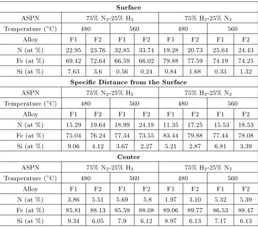
To know whether nitrided phases were coated on the surface and diused into the ribbons, the concentration of alloying elements containing nitrogen were analyzed along the thickness direction using EDS (Table 3). As could be seen, EDS analysis shows the presence of Fe and N on the surface of the ribbons which is generally referred to the compound layer, but a low Si content on the surface could be detected except for 480C and in 75% N
2-25% H2 gas mixture,
indicating the discontinuous compound layer. EDS demonstrated the presence of Fe, Si and N in the diusion zone. It is expected that the diusion of nitrogen from the surface to the interior is observed depending on the temperature, time and the chemical composition of the base material [22]. The concentra-tion of nitrogen in the compound layer is more than that of the diusion zone. Comparing the nitrogen content of the surface and bulk of the nitrided F1 alloy with that of the nitrided F2 alloy, it could be seen that the nitrogen concentration on the surface of both ribbons with the same gas mixture are almost similar at 480C and 560C. But it is more for F2 alloy
compared to F1 alloy in the bulk of the ribbons, since Table 2. The intergranular distance for F1 and F2 alloys, (nm)a.
Temperature
(C) ASPN: 75% N2-25% H2 ASPN: 25% N2-75% H2 Annealed
F1 F2 F1 F2 F1 F2
410 0.90 1.71 0.97 1.93 1.00 2.79
440 0.85 1.35 1.05 1.58 1.24 2.45
480 0.63 0.80 0.74 0.91 1.21 1.60
520 0.6 0.64 0.76 0.78 1.17 1.56
560 0.27 0.34 0.33 0.46 0.88 1.21
Table 3. EDS results for F1 and F2 nitrided ribbonsa.
Surface
ASPN 75% N2-25% H2 75% H2-25% N2
Temperature (C) 480 560 480 560
Alloy F1 F2 F1 F2 F1 F2 F1 F2
N (at %) 22.95 23.76 32.85 33.74 19.28 20.73 25.64 24.43 Fe (at %) 69.42 72.64 66.59 66.02 79.88 77.59 74.19 74.25
Si (at %) 7.63 3.6 0.56 0.24 0.84 1.68 0.33 1.32
Specic Distance from the Surface
ASPN 75% N2-25% H2 75% H2-25% N2
Temperature (C) 480 560 480 560
Alloy F1 F2 F1 F2 F1 F2 F1 F2
N (at %) 15.29 19.64 18.99 24.18 11.35 17.25 15.53 18.53 Fe (at %) 75.04 76.24 77.34 73.55 83.44 79.88 77.44 78.08
Si (at %) 9.06 4.12 3.67 2.27 5.21 2.87 6.81 3.39
Center
ASPN 75% N2-25% H2 75% H2-25% N2
Temperature (C) 480 560 480 560
Alloy F1 F2 F1 F2 F1 F2 F1 F2
N (at %) 3.86 5.51 5.69 5.8 1.97 3.10 5.32 5.39
Fe (at %) 85.81 88.13 85.59 88.08 89.06 89.77 86.53 88.47
Si (at %) 9.34 6.05 7.9 6.12 8.97 6.13 7.17 6.13
a: Estimated error is 2%
F2 alloy contains higher crystalline volume fraction and lower amount of Nb content which could play a barrier role in diusion of nitrogen because of the large atomic radius of niobium [8]. The second important result from Table 3 which deserves attention is that the nitrogen content on the surface of the ribbons for both alloys is higher in 75% N2-25% H2 gas mixture
than in 75% H2-25% N2 in which it contains more
Fe2 3N phase than Fe4N according to the XRD results.
Moreover, the nitrogen concentration in the bulk of both alloys increases with the increasing of the nitriding temperature and nitrogen content in the gas mixture.
Figure 8 shows AFM images of the surfaces of nitrided F1 and F2 alloys which according to the EDS results, corresponds to the iron nitrides. It is signicant to note that the mean grain size of the iron nitrides on
Figure 9. AFM images of the annealed (a) F2 and (b) F1 ribbons at 480C.
the surface of the F1 alloy is smaller than that of the F2 alloy. It is probably due to the Si-N precipitates on the surface of the ribbons which act as nucleation centers. The more Si content in F1 alloy and, consequently, the more Si-N precipitates on the surface of the ribbons regarding the completion of nanocrystallization on the surface, lead to ner grain size of the iron nitrides. The images for annealed samples show that the crystalliza-tion at the surface level is fully completed (Figure 9); meanwhile in the XRD patterns there is no evidence of any reection belonging to FeB phases which are the nal products of the crystallization process. This fact conrms that the crystallization process is dierent in the surface of the samples than in the bulk. It is expected that crystallization process is quicker at the surface [23]. The mean grain size of these nanograins and nitrides estimated from AFM images are compared with the corresponding one obtained by XRD patterns, achieving a good agreement between the two techniques in both cases.
Figure 10 shows the electrical resistivity of the annealed and nitrided F2 alloy. For comparison of both alloys, it can be noted that the grain size of Fe(Si) phase
Figure 10. Temperature dependence of the electrical resistivity for F2 alloy.
and the Si content within Fe(Si) play a vital role in the resistivity at nanostate where nanoparticles of Fe(Si) are dispersed in amorphous matrix [19]. Accordingly, the decrease of electrical resistivity for the annealed and nitrided F2 alloy compared to the F1 alloy [14] at temperatures above 410C is due to the larger grain size
and lower Si content in Fe(Si) phase of this alloy. At 410C, resistivity is lower for the annealed and nitrided
F1 alloy [14], although particle size of the nanophase is smaller than that for the annealed and nitrided F2 alloy. It is due to the lower Si content in Fe(Si) nuclei for both annealed and nitrided F1 alloy and the absence of the nitrided phases in the diusion layer of nitrided F1 alloy. After formation of nanocrystalline phase, resistivity is found to be increased. It is generally accounted that in nanocrystalline alloys, the rise in resistivity after nanocrystallization is due to the grain boundary scattering by the crystallization and nanoparticles [19]. The formation of boride phases such as Fe2B and full nanocrystallization in the annealed
F2 alloy are responsible for the decrease in resistivity. Also for both nitrided ribbons, the electrical resistivity is higher than that for the annealed samples due to the formation of iron nitrides and nitrided phases such as Si-N precipitates, Nb2N and NbN which have high
elec-trical resistivity. In contrast to the annealed samples, electrical resistivity increases at higher temperatures in the nitrided samples.
Figure 11 shows the plot of hardness versus temperature from the bulk of the F2 ribbon. The increase in hardness for F2 alloy compared to the F1 alloy at 410C is mainly due to the nanocrystallization
process and presence of Fe(Si) phase with nanometeric grains. As annealing temperature increases to 520C,
hardness values increase for both alloys. But the larger grain size of Fe(Si) phase and higher crystalline volume fraction in F2 alloy result in a higher hardness value than F1 alloy [14]. At 560C, more decrease
of the hardness value could be seen for F2 alloy due to the lower second crystallization temperature and consequently, more grain growth. In ASPN treatment, nitrogen is mainly incorporated into the existing iron lattice as interstitial atoms or as nely dispersed alloy nitride precipitates. It is possible to say that hardening
Figure 11. Bulk micro-hardness versus temperature for F2 alloy.
in the diusion layer is caused by the microstrain in the matrix induced by the formation of coherent precipitated phase [15]. Moreover, nitrogen atoms located in interstitial positions cause solid solution hardening, thus increase the hardness of the samples. The higher amount of hardness value for nitrided F2 alloy, compared to the F1 alloy, is due to the same reasons mentioned for the annealed samples and also the more nitrogen diusion into the F2 ribbons as well as the formation of more Fe4N phase.
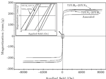
The magnetic properties in the nanocrystalline FeSiNbBCu alloys are dominated by the structure which depends on compositions and annealing con-ditions. It is signicant for application to improve the soft magnetic properties in the nanostructured FeSiNbBCu alloys with high saturation magnetization (Ms) [23]. The room temperature hysteresis loops of F2
alloy were measured (Figure 12). As shown, both the coercivity (Hc) and Ms increase after the nitrication
process. The Ms of the heat treated F2 sample was,
however, higher than that of the F1 sample which has been previously reported [14]. This is related to the higher Fe content in F2 alloy. The formation of more Fe4N nitrides also leads to the increase of Ms for the
nitrided F2 alloy, compared to the nitrided F1 alloy. As could be seen, for nitrided F2 alloy, by using 75% H2-25% N2 gas mixture, Ms is higher with respect to
75% N2-25% H2 gas mixture. It is interesting to note
that the Hc of the samples containing Fe3Si phase is
lower by an order of magnitude, as compared to the samples containing -Fe(Si) phase [5]. Accordingly, the Hc decreases with increasing Si content in amorphous
and partially crystallized phases. Due to this fact, it increases from F1 to F2 alloy in both annealed and nitrided samples. At 440C, despite the nitrided F1
sample, the Hc is higher in nitrided F2 sample with
higher amount of nitrogen content in the nitriding gas mixture. At this temperature, the nanocrystallization
Figure 12. Magnetization curve for nitrided and annealed F2 at 440C.
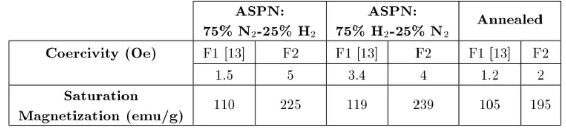
Table 4. The values of Ms and Hcfor dierent samples at 440C.
ASPN: 75% N2-25% H2
ASPN:
75% H2-25% N2 Annealed
Coercivity (Oe) F1 [13] F2 F1 [13] F2 F1 [13] F2
1.5 5 3.4 4 1.2 2
Saturation
Magnetization (emu/g) 110 225 119 239 105 195
of Fe(Si) phase, diusion of nitrogen into the Fe(Si) grains and, therefore, the formation of Fe4N nitrides
take place. These could be resulted in the higher amount of Hc for F2 nitrided in 75% N2-25% H2 gas
mixture than that in 75% H2-25% N2. But for F1
nitrided in 75% H2-25% N2 gas mixture, Hc is more
than that in 75% N2-25% H2 gas mixture. The values
of Ms and Hc for F1 and F2 alloys are presented in
Table 4.
CONCLUSIONS
1. A comparative study of nanocrystallization of two series of Finemet alloys with dierent compositions after active screen plasma nitriding and annealing at dierent temperatures was made. Nitriding of Fe73:5Si13:5B9Nb3Cu1and Fe77Si11B9Nb2:4Cu0:6
alloys led to the decrease of Fe(Si) grain size and increase of the crystalline volume fraction.
2. The smaller amount of Nb shifted the onset crystallization temperatures towards lower tem-peratures, leading to the larger grain size of Fe(Si) phase and higher crystalline volume frac-tion in each temperature for both nitrided and annealed Fe77Si11B9Nb2:4Cu0:6 samples compared
to Fe73:5Si13:5B9Nb3Cu1alloy.
3. ASPN treatment caused an increase of the lattice parameter for a part of the Fe(Si) phase where nitrogen has diused. The superior nitriding poten-tial is demonstrated by the larger lattice parameter of that part of the Fe(Si) phase. At temperatures which the nanocrystallization of both alloys takes place, the lattice parameter of Fe(Si) phase for Fe77Si11B9Nb2:4Cu0:6 alloy was larger than that
for Fe73:5Si13:5B9Nb3Cu1 alloy due to the lower Si
content in Fe77Si11B9Nb2:4Cu0:6 alloy and
conse-quently, in Fe(Si) phase.
4. The mean grain size of the iron nitrides on the sur-face of the Fe73:5Si13:5B9Nb3Cu1 alloy was smaller
than that of the Fe77Si11B9Nb2:4Cu0:6 alloy. It is
believed that this is related to the higher amount of Si-N precipitates as a nucleation centers on the surface of the Fe73:5Si13:5B9Nb3Cu1ribbons.
5. ASPN treatment increased the electrical resistivity of alloys. The larger grain size and lower Si content
in Fe(Si) phase for Fe77Si11B9Nb2:4Cu0:6 alloy gave
rise to a decrease of electrical resistivity compared to Fe73:5Si13:5B9Nb3Cu1alloy.
6. It was concluded that nitriding increased the hard-ness of alloys. The highest hardhard-ness was achieved for nitrided Fe77Si11B9Nb2:4Cu0:6alloy at 560C in
75% N2-25% H2gas mixture.
7. Comparison of magnetic results for both al-loys showed that the maximum saturation mag-netization and coercivity were obtained for Fe77Si11B9Nb2:4Cu0:6 alloy after nitriding under
75% H2-25% N2 and 75% N2-25% H2 gas mixture
at 440C, respectively.
REFERENCES
1. Ferna'ndez, L. et al. \Magnetic behavior and mi-crostructure of Finemet-type ribbons in both, surface and bulk", Journal of Non-Crystalline Solids, 353, pp. 777-781 (2007).
2. Manivel Raja, M. et al. \Structure and soft magnetic properties of Finemet alloys", Journal of Alloys and Compounds, 297, pp. 199-205 (2000).
3. Herzer, G., Handbook of Magnetic Materials, K.H.J. Buschow, Eds., 10, pp. 415-462, Elsevier, Amsterdam (1997).
4. Raszka, T. and Przybyl, A. \Optimisation of soft mag-netic properties in Fe83 XCoXNb3B13Cu1 (x=10, 30,
40) amorphous alloys", 13th International Scientic Conference on Achievements in Mechanical and Ma-terials Engineering, Gliwice, Poland, 16th-18th May (2005).
5. Majumdar, B. and Akhtar, D. \Structure and coerciv-ity of nanocrystalline Fe-Si-B-Nb-Cu alloys", Journal of Bull. Mater. Sci., 28(5), pp. 395-399 (2005). 6. Li, C. et al. \Crystallization behavior of co-containing
FINEMET amorphous alloy melt-spun ribbon", Jour-nal of Materials Letters, 60, pp. 309-312 (2006). 7. Iturriza, N. et al. \Nanostructure and magnetic
prop-erties of Ni-substituted Finemet ribbons", Journal of Magnetism and Magnetic Materials, 316(2), pp. 74-77 (2007).
8. Atmani, H. et al. \Crystallization-nitriding process of FeSiB and FeSiBCuNb ribbons: Inuence of additive (Cu, Nb) pair and nitrogen on structure magnetic
and magnetostrictive parameters", Journal of Non-Crystalline Solids, 290, pp. 194-207 (2001).
9. Atmani, H. and Thoumire, O. \Microstructure char-acterization of uidized bed nitride Fe-Si and Fe-Si-Al foils", Bull. Mater. Sci., 25, pp. 219-225 (2002). 10. Alves, C. Jr. et al. \Use of cathodic cage in plasma
nitriding", Journal of Surface Coating & Technology, 201, pp. 2450-2454 (2006).
11. Wang, L. et al. \Plasma nitriding of low alloy steels at oating and cathodic potentials", Journal of Applied Surface Science, 254, pp. 6595-6600 (2008).
12. de Sousa, R.R.M. et al. \Cathodic cage nitriding of samples with dierent dimensions", Journal of Ma-terial Science and Engineering A, 465, pp. 223-227 (2007).
13. Zhao, C. et al. \Study on the activate plasma nitriding and its nitriding mechanism", Journal of Surface & Coatings Technology, 201, pp. 2320-2325 (2006). 14. Shivaee, H.A. et al. \Study of nanocrystallization in
FINEMET alloy by active screen plasma nitriding", Journal of Alloys and Compound, 491(1-2), pp. 487-494 (2009).
15. Turk, A. et al. \Structural characterization of uidized bed nitrided steels", Journal of Vacuum, 80, pp. 332-342 (2005).
16. Grognet, S. et al. \Microstructural study of nanocrys-talline Fe-(Cu-Nb)-Si-B ribbons obtained by a nitrid-ing thermochemical treatment", Journal of Magnetism and Magnetic Materials, 210, pp. 167-180 (2000). 17. Atmani, H. et al. \Nitriding thermochemical treatment
and Niobium dual eect on nanocrystallization FeSi-BCu ribbons", Journal of Scripta Mater., 42, pp. 117-122 (2000).
18. Grognet, S. et al. \The inuence of nitrogen on the structural and magnetic properties of nanocrystallized Finemet-type ribbons", Journal of Magnetism and Magnetic Materials, 203, pp. 172-174 (1999).
19. Panda, A.K. et al. \Crystallization and soft magnetic properties of rapidly solidied Fe73:5Nb3Cu1Si22:5 X
BX (X=5,9,10,11,19) alloys", Journal of Magnetism
and Magnetic Materials, 260, pp. 70-77 (2003). 20. Cziraki, A. et al. \Some structural aspects of magnetic
property evolution in Finemet-type sensor material during amorphous-nanocrystalline transformations", Journal of Periodica Polytechnica Ser. Transp. Eng., 47, pp. 167-176 (2004).
21. Crisan, O. et al. \Nanocrystallization of soft magnetic Finemet-type amorphous ribbons", Journal of Sensors and Actuators A, 106, pp. 246-250 (2003).
22. Usta, M. et al. \Nitriding of AISI 316L surgical stainless steel in uidized bed reactor", Journal of Vacuum, 73, pp. 505-510 (2004).
23. Yoshizawa, Y. \Magnetic properties and applications of nanostructured soft magnetic materials", Journal of Scripta Mater., 44, pp. 1321-1325 (2001).
BIOGRAPHIES
Elmira Memarzadeh Lotfabad completed his B.S. and M.S. studies in the Materials Science and Engineer-ing at Tehran University and Sharif University of Tech-nology, respectively, in 2009. She is currently working on research papers in the eld of Nanostructures. She has ranked 1th among all M.S. Materials Selection and Processing students based on overall GPA at Sharif University of Technology.
Hamid Reza Madaah Hosseini is a professor of Materials Science and Engineering at Sharif University of Technology. He received his Ph.D. in Advanced Ma-terials from Sharif University of Technology in 2000 and was appointed as a member of Scientic Committee in the Department. He is currently working as a member in Institute for Nanoscience and Nanotechnology at Sharif University of Technology. His eld of research is Magnetic Materials and Nanostructures and has published a lot of papers in this eld.
Hossein Asghari Shivaee received his B.S. in the Mining and Metallurgical Engineering from Amir Kabir University of Technology in 2002 and M.S. and Ph.D. in Nanosience and Technology-Nanomaterials from Sharif University of Technology in 2010. He is currently working in Institute for Nanoscience and Nanotech-nology and doing some research work in the eld of Nanotechnology.
Saied Roostaie received his B.S. in the Mining and Metallurgical Engineering in 2002 from Amir Kabir University of Technology. He is currently working in Research Centers related to Metallurgical Engineering in Tehran.