M
AN228
INTRODUCTION
Many network protocols are described using the seven layer Open System Interconnection (OSI) model, as shown in Figure 1. The Controller Area Network (CAN) protocol defines the Data Link Layer and part of the Physical Layer in the OSI model. The remaining physi-cal layer (and all of the higher layers) are not defined by the CAN specification. These other layers can either be defined by the system designer, or they can be imple-mented using existing non-proprietary Higher Layer Protocols (HLPs) and physical layers.
The Data Link Layer is defined by the CAN specifica-tion. The Logical Link Control (LLC) manages the over-load control and notification, message filtering and recovery management functions. The Medium Access Control (MAC) performs the data encapsulation/decap-sulation, error detection and control, bit stuffing/de-stuffing and the serialization and deserialization functions.
The Physical Medium Attachment (PMA) and Medium Dependent Interface (MDI) are the two parts of the physical layer which are not defined by CAN. The Physical Signaling (PS) portion of the physical layer is defined by the CAN specification. The system designer can choose any driver/receiver and transport medium as long as the PS requirements are met.
The International Standards Organization (ISO) has defined a standard which incorporates the CAN speci-fication as well as the physical layer. The standard, ISO-11898, was originally created for high-speed in-vehicle communications using CAN. ISO-11898 speci-fies the physical layer to ensure compatibility between CAN transceivers.
A CAN controller typically implements the entire CAN specification in hardware, as shown in Figure 1. The PMA is not defined by CAN, however, it is defined by ISO-11898. This document discusses the MCP2551 CAN transceiver and how it fits in with the ISO-11898 specification.
FIGURE 1: CAN AND THE OSI MODEL
Author: Pat Richards
Microchip Technology Inc.
Physical Application Presentation
Session Transport
Network Data Link
Physical Medium Attachment Physical Signaling
Medium Dependent Interface - Bit encoding/decoding - Bit timing/synchronization - Driver/receiver characteristics
- Connectors/wires Logical Link Control (LLC)
Medium Access Control (MAC) - Data encapsulation/decapsulation
- Acceptance filtering - Overload notification - Recovery management
- Frame coding (stuffing/de-stuffing) - Error detection/signaling
- Serialization/deserialization
Defined by
ISO11898 7- Layer OSI
CAN Controller
Transceiver MCP2551
AN228
ISO11898-2 OVERVIEW
ISO11898 is the international standard for high-speed CAN communications in road vehicles. ISO-11898-2 specifies the PMA and MDA sublayers of the Physical Layer. See Figure 3 for a representation of a common CAN node/bus as described by ISO-11898.
Bus Levels
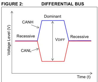
CAN specifies two logical states: recessive and domi-nant. ISO-11898 defines a differential voltage to repre-sent recessive and dominant states (or bits), as shown in Figure 2.
In the recessive state (i.e., logic ‘1’ on the MCP2551 TXD input), the differential voltage on CANH and CANL is less than the minimum threshold (<0.5V receiver input or <1.5V transmitter output)(See Figure 4). In the dominant state (i.e., logic ‘0’ on the MCP2551 TXD input), the differential voltage on CANH and CANL is greater than the minimum threshold. A dominant bit overdrives a recessive bit on the bus to achieve nondestructive bitwise arbitration.
FIGURE 2: DIFFERENTIAL BUS
Connectors and Wires
ISO-11898-2 does not specify the mechanical wires and connectors. However, the specification does require that the wires and connectors meet the electri-cal specification.
The specification also requires 120Ω (nominal) termi-nating resistors at each end of the bus. Figure 3 shows an example of a CAN bus based on ISO-11898.
FIGURE 3: CAN BUS
V
ol
tage Lev
el
(
V
)
Time (t) VDIFF
Dominant
Recessive Recessive
CANH
CANL
120Ω 120Ω
MCU
CAN Controller
Transceiver
AN228
FIGURE 4: ISO11898 NOMINAL BUS LEVELS
Robustness
The ISO11898-2 specification requires that a compliant or compatible transceiver must meet a number of elec-trical specifications. Some of these specifications are intended to ensure the transceiver can survive harsh electrical conditions, thereby protecting the
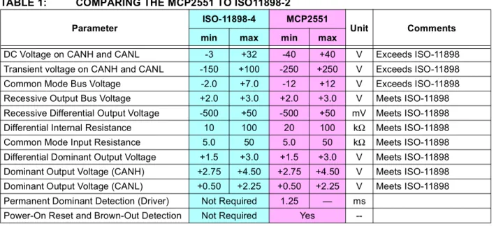
communications of the CAN node. The transceiver must survive short circuits on the CAN bus inputs from -3V to +32V and transient voltages from -150V to +100V. Table 1 shows the major ISO11898-2 electrical requirements, as well as MCP2551 specifications.
TABLE 1: COMPARING THE MCP2551 TO ISO11898-2 2.5
3.5
1.5
0.9 5.0
0.5
-1.0 -0.5
0.05 1.5 3.0 V
V V
Recessive Differential Input Range Dominant Differential Input Range Dominant
Differential Output Range
Recessive Differential Output Range
CANH
CANL
Parameter ISO-11898-4 MCP2551 Unit Comments min max min max
DC Voltage on CANH and CANL -3 +32 -40 +40 V Exceeds ISO-11898
Transient voltage on CANH and CANL -150 +100 -250 +250 V Exceeds ISO-11898
Common Mode Bus Voltage -2.0 +7.0 -12 +12 V Exceeds ISO-11898
Recessive Output Bus Voltage +2.0 +3.0 +2.0 +3.0 V Meets ISO-11898 Recessive Differential Output Voltage -500 +50 -500 +50 mV Meets ISO-11898 Differential Internal Resistance 10 100 20 100 kΩ Meets ISO-11898
Common Mode Input Resistance 5.0 50 5.0 50 kΩ Meets ISO-11898
Differential Dominant Output Voltage +1.5 +3.0 +1.5 +3.0 V Meets ISO-11898 Dominant Output Voltage (CANH) +2.75 +4.50 +2.75 +4.50 V Meets ISO-11898 Dominant Output Voltage (CANL) +0.50 +2.25 +0.50 +2.25 V Meets ISO-11898 Permanent Dominant Detection (Driver) Not Required 1.25 — ms
--AN228
Bus Lengths
ISO11898 specifies that a transceiver must be able to drive a 40m bus at 1 Mb/s. A longer bus length can be achieved by slowing the data rate. The biggest limita-tion to bus length is the transceiver’s propagalimita-tion delay.
PROPAGATION DELAY
The CAN protocol has defined a recessive (logic ‘1’) and dominant (logic ‘0’) state to implement a non-destructive bit-wise arbitration scheme. It is this arbitra-tion methodology that is affected most by propagaarbitra-tion delays. Each node involved with arbitration must be able to sample each bit level within the same bit time. For example, if two nodes at opposite ends of the bus start to transmit their messages at the same time, they must arbitrate for control of the bus. This arbitration is only effective if both nodes are able to sample during
the same bit time. Figure 5 shows a one-way propaga-tion delay between two nodes. Extreme propagapropaga-tion delays (beyond the sample point) will result in invalid arbitration. This implies that bus lengths are limited at given CAN data rates.
A CAN system’s propagation delay is calculated as being a signal’s round-trip time on the physical bus (tbus), the output driver delay (tdrv) and the input com-parator delay (tcmp). Assuming all nodes in the system have similar component delays, the propagation delay is explained mathematically:
EQUATION 1:
FIGURE 5: ONE-WAY PROPAGATION DELAY
tprop = 2⋅(tbus tcmp tdrv+ + )
SyncSeg
Sample Point
SyncSeg
Transmitted Bit from “Node A”
“Node A” bit received by “Node B”
Propagation Delay
Time (t)
PropSeg PhaseSeg1 (PS1) PhaseSeg2 (PS2)
AN228
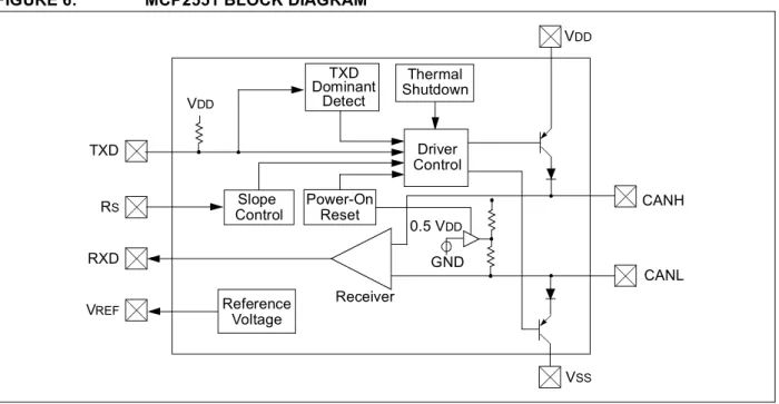
MCP2551 CAN TRANSCEIVER
The MCP2551 is a CAN Transceiver that implements the ISO-11898-2 physical layer specification. It sup-ports a 1 Mb/s data rate and is suitable for 12 V and 24 V systems. The MCP2551 provides short-circuit protection up to ±40V and transient protection up to ±250V.
In addition to being ISO-11898-2-compatible, the MCP2551 provides power-on reset and brown-out pro-tection, as well as permanent dominant detection to ensure an unpowered or faulty node will not disturb the bus. The device implements configurable slope control on the bus pins to help reduce RFI emissions. Figure 6 shows the block diagram of the MCP2551.
General MCP2551 Operation
TRANSMIT
The CAN protocol controller outputs a serial data stream to the logic TXD input of the MCP2551. The cor-responding recessive or dominant state is output on the CANH and CANL pins.
RECEIVE
The MCP2551 receives dominant or recessive states on the same CANH and CANL pins as the transmit occurs. These states are output as logic levels on the RXD pin for the CAN protocol controller to receive CAN frames.
RECESSIVE STATE
A logic ‘1’ on the TXD input turns off the drivers to the CANH and CANL pins and the pins “float” to a nominal 2.5V via biasing resistors.
DOMINANT STATE
A logic ‘0’ on the TXD input turns on the CANH and CANL pin drivers. CANH drives ~1V higher than the nominal 2.5V recessive state to ~3.5V. CANL drives ~1V less than the nominal 2.5V recessive state to ~1.5V.
FIGURE 6: MCP2551 BLOCK DIAGRAM
VDD
VSS
CANH
CANL TXD
RS RXD VREF
VDD
Slope
Control Power-OnReset
Reference Voltage
Receiver
GND 0.5 VDD TXD
Dominant Detect
Thermal Shutdown
Driver Control
AN228
Modes of Operation
There are three modes of operation that are externally controlled via the RS pin:
1. High-Speed 2. Slope Control 3. Standby
HIGH-SPEED
The high-speed mode is selected by connecting the RS pin to VSS. In this mode, the output drivers have fast rise and fall times that support the higher bus rates up to 1 Mb/s and/or maximum bus lengths by providing the minimum transceiver loop delays.
SLOPE CONTROL
If reduced EMI is required, the MCP2551 can be placed in slope control mode by connecting a resistor (REXT) from the RS pin to ground. In slope control mode, the single-ended slew rate (CANH or CANL) is basically proportional to the current out of the RS pin. The current must be in the range of 10 µA < -IRS < 200 µA, which corresponds to a voltage on the pin of 0.4 VDD < VRS < 0.6 VDD respectively (or 0.5 VDD typical).
The decreased slew rate implies a slower CAN data rate at a given bus length, or a reduced bus length at a given CAN data rate.
STANDBY
Standby (or sleep) mode is entered by connecting the RS pin to VDD. In sleep mode, the transmitter is switched off and the receiver operates in a reduced power mode. While the receive pin (RXD) is still functional, it will operate at a slower rate.
Standby mode can be used to place the device in low power mode and to turn off the transmitter in case the CAN controller malfunctions and sends unexpected data to the bus.
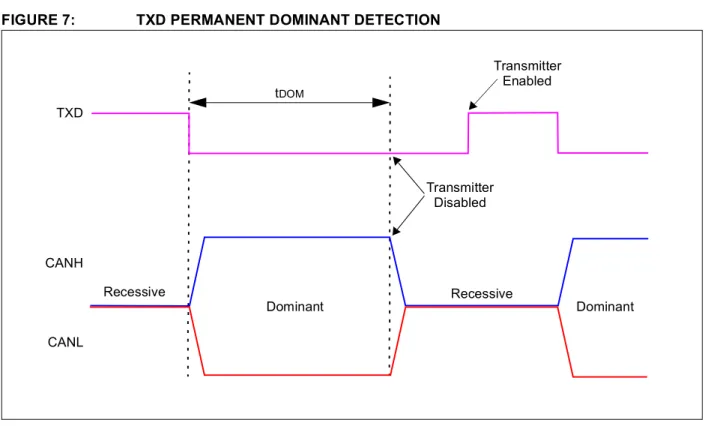
Permanent Dominant Detection on
Transmitter
The MCP2551 will turn off the transmitter to CANH and CANL if an extended dominant state is detected on the transmitter. This ability prevents a faulty node (CAN controller or MCP2551) from permanently corrupting the CAN bus.
The drivers are disabled if TXD is low for more than ~1.25 ms (minimum) (See Figure 7).
The drivers will remain disabled as long as TXD remains low. A rising edge on TXD will reset the timer logic and enable the drivers.
FIGURE 7: TXD PERMANENT DOMINANT DETECTION
Dominant Recessive
tDOM
Transmitter Disabled
Transmitter Enabled
Recessive
Dominant TXD
CANH
AN228
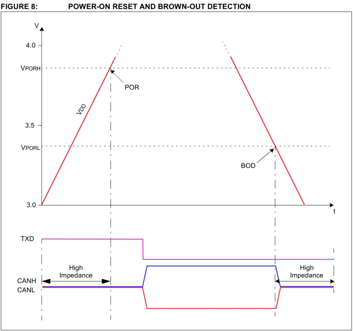
Power-On Reset and Brown-Out
The MCP2551 incorporates both Power-On Reset (POR) and Brown-Out Detection (BOD) (see Figure 8).
POWER-ON RESET (POR)
When the MCP2551 is powered on, the CANH and CANL pins remain in the high impedance state until VDD reaches the POR high voltage (VPORH). Additionally, if the TXD pin is low at power-up, the
CANH and CANL pins will remain in high impedance until TXD goes high. After which, the drivers will function normally.
BROWN-OUT DETECTION (BOD)
BOD occurs when VDD goes below the power-on reset low voltage (VPORL). At this point, the CANH and CANL pins enter a high impedance state and will remain there until VPORH is reached.
FIGURE 8: POWER-ON RESET AND BROWN-OUT DETECTION
3.0 3.5
4.0 V
t
TXD
CANH CANL
High
Impedance ImpedanceHigh
VPORH
VPORL
VDD
POR
AN228
Ground Offsets
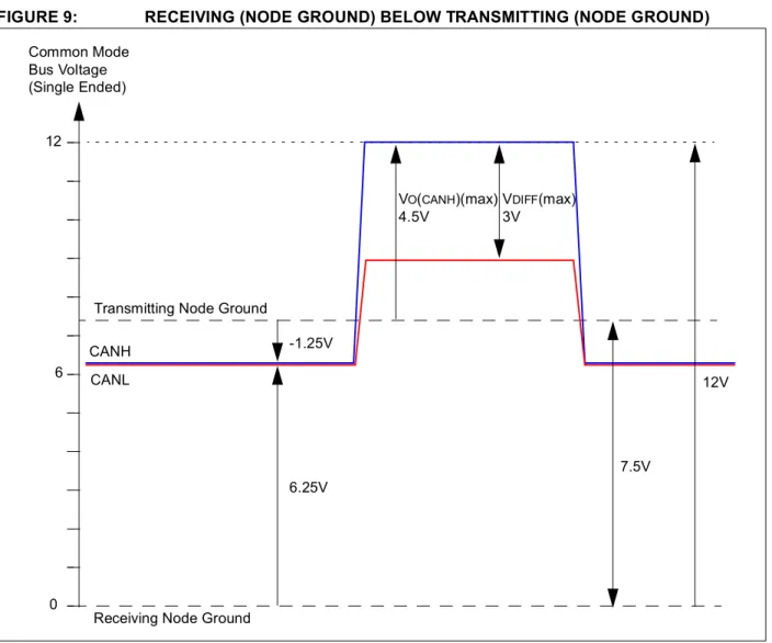
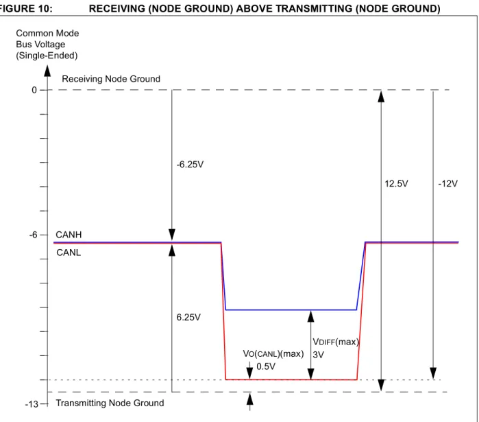
Since it is not required to provide a common ground between nodes, it is possible to have ground offsets between nodes. That is, each node may observe differ-ent single-ended bus voltages (common mode bus voltages) while maintaining the same differential volt-age. While the MCP2551 is specified to handle ground offsets from -12V to +12V, the ISO-11898 specification only requires -2V to +7V. Figure 9 and Figure 10 demonstrate how ground offsets appear between nodes.
Figure 9 shows the transmitting node with a positive ground offset with respect to the receiving node. The MCP2551 receiver can operate with CANH = +12V. The maximum CAN dominant output voltage (VO(CANH)) from the transmitting node is 4.5V. Subtract-ing this maximum yields an actual ground offset (with respect to the receiving node) of 7.5V for the transmit-ting node. In the recessive state, each node attempts to pull the CANH and CANL pins to their biasing levels
(2.5V typical). However, the resulting common mode voltage in the recessive state becomes 6.25V for the receiving node and -1.25V for the transmitting node. Figure 10 shows the transmitting node with a negative ground offset with respect to the receiving node. The MCP2551 receiver can operate with CANL = -12V. The minimum CAN dominant output voltage (VO(CANL)) from the transmitting node is 0.5V. Subtracting this min-imum yields an actual ground offset, with respect to the receiving node, of -12.5V. The common mode voltage for the recessive state is -6.25V for the receiving node and 6.25V for the transmitting node.
Since all nodes act as a transmitter for a portion of each message (i.e., each receiver must acknowledge (ACK) valid messages during the ACK slot), the largest ground offset allowed between nodes is 7.5V, as shown in Figure 9.
Operating a CAN system with large ground offsets can lead to increased electromagnetic emissions. Steps must be taken to eliminate ground offsets if the system is sensitive to emissions.
FIGURE 9: RECEIVING (NODE GROUND) BELOW TRANSMITTING (NODE GROUND) Common Mode
Bus Voltage (Single Ended)
Transmitting Node Ground
Receiving Node Ground 0
6 12
CANH CANL
VDIFF(max) 3V
VO(CANH)(max) 4.5V
6.25V -1.25V
7.5V
AN228
FIGURE 10: RECEIVING (NODE GROUND) ABOVE TRANSMITTING (NODE GROUND)
BUS TERMINATION
Bus termination is used to minimize signal reflection on the bus. ISO-11898 requires that the CAN bus have a nominal characteristic line impedance of 120Ω. There-fore, the typical terminating resistor value for each end of the bus is 120Ω. There are a few different termination methods used to help increase EMC performance (see Figure 11).
1. Standard Termination 2. Split Termination 3. Biased Split Termination
Standard Termination
As the name implies, this termination uses a single 120Ω resistor at each end of the bus. This method is acceptable in many CAN systems.
Split Termination
Split termination is a concept that is growing in popular-ity because emission reduction can be achieved very easily. Split termination is a modified standard termina-tion in which the single 120Ω resistor on each end of the bus is split into two 60Ω resistors, with a bypass capacitor tied between the resistors and to ground. The two resistors should match as close as possible. Common Mode
Bus Voltage (Single-Ended)
Transmitting Node Ground Receiving Node Ground
-13 -6 0
CANH CANL
VDIFF(max) 6.25V
-6.25V
12.5V -12V
3V VO(CANL)(max)
0.5V
Note: EMC performance is not determined solely by the transceiver and termination method, but rather by careful consideration of all components and topology of the system.
AN228
Biased Split Termination
This termination method is used to maintain the com-mon mode recessive voltage at a constant value, thereby increasing EMC performance. This circuit is the same as the split termination with the addition of a voltage divider circuit to achieve a voltage of VDD/2 between the two 60Ω resistors (see Figure 11).
FIGURE 11: TERMINATION CONCEPTS
REFERENCES
MCP2551 Data Sheet, “High Speed CAN Transceiver”, DS21667, Microchip Technology, Inc.
AN754, “Understanding Microchip’s CAN Module Bit Timing”, DS00754, Microchip Technology, Inc.
ISO-11898-2, “Road Vehicles - Interchange of Digital Information - Part 2: High Speed Medium Access Unit and Medium Dependant Interface”, International Organization for Standardization.
CAN System Engineering, “From Theory to Practical Applications”, Wolfhard Lawrenz, Springer.
Note: The biasing resistors in Figure 11, as well as the split termination resistors, should match as close as possible.
Standard Termination
Split Termination
Biased Termination Split 120Ω
60Ω 60Ω
60Ω 60Ω R1
R2 C
Information contained in this publication regarding device applications and the like is intended through suggestion only and may be superseded by updates. It is your responsibility to ensure that your application meets with your specifications. No representation or warranty is given and no liability is assumed by Microchip Technology Incorporated with respect to the accuracy or use of such information, or infringement of patents or other intellectual property rights arising from such use or otherwise. Use of Microchip’s products as critical com-ponents in life support systems is not authorized except with express written approval by Microchip. No licenses are con-veyed, implicitly or otherwise, under any intellectual property rights.
Trademarks
The Microchip name and logo, the Microchip logo, KEELOQ, MPLAB, PIC, PICmicro, PICSTART and PRO MATE are registered trademarks of Microchip Technology Incorporated in the U.S.A. and other countries.
FilterLab, microID, MXDEV, MXLAB, PICMASTER, SEEVAL and The Embedded Control Solutions Company are registered trademarks of Microchip Technology Incorporated in the U.S.A.
dsPIC, dsPICDEM.net, ECONOMONITOR, FanSense, FlexROM, fuzzyLAB, In-Circuit Serial Programming, ICSP, ICEPIC, microPort, Migratable Memory, MPASM, MPLIB, MPLINK, MPSIM, PICC, PICDEM, PICDEM.net, rfPIC, Select Mode and Total Endurance are trademarks of Microchip Technology Incorporated in the U.S.A. and other countries. Serialized Quick Turn Programming (SQTP) is a service mark of Microchip Technology Incorporated in the U.S.A.
All other trademarks mentioned herein are property of their respective companies.
© 2002, Microchip Technology Incorporated, Printed in the U.S.A., All Rights Reserved.
Printed on recycled paper.
Microchip received QS-9000 quality system certification for its worldwide headquarters, design and wafer fabrication facilities in Chandler and Tempe, Arizona in July 1999 and Mountain View, California in March 2002. The Company’s quality system processes and procedures are QS-9000 compliant for its PICmicro®8-bit MCUs, KEELOQ®code hopping devices, Serial EEPROMs, microperipherals, non-volatile memory and analog products. In addition, Microchip’s quality system for the design and manufacture of development
Note the following details of the code protection feature on Microchip devices:
• Microchip products meet the specification contained in their particular Microchip Data Sheet.
• Microchip believes that its family of products is one of the most secure families of its kind on the market today, when used in the intended manner and under normal conditions.
• There are dishonest and possibly illegal methods used to breach the code protection feature. All of these methods, to our knowl-edge, require using the Microchip products in a manner outside the operating specifications contained in Microchip's Data Sheets. Most likely, the person doing so is engaged in theft of intellectual property.
• Microchip is willing to work with the customer who is concerned about the integrity of their code.
• Neither Microchip nor any other semiconductor manufacturer can guarantee the security of their code. Code protection does not mean that we are guaranteeing the product as “unbreakable.”
Code protection is constantly evolving. We at Microchip are committed to continuously improving the code protection features of our products.
M
AMERICASCorporate Office
2355 West Chandler Blvd. Chandler, AZ 85224-6199
Tel: 480-792-7200 Fax: 480-792-7277 Technical Support: 480-792-7627 Web Address: http://www.microchip.com
Rocky Mountain
2355 West Chandler Blvd. Chandler, AZ 85224-6199
Tel: 480-792-7966 Fax: 480-792-4338
Atlanta
500 Sugar Mill Road, Suite 200B Atlanta, GA 30350
Tel: 770-640-0034 Fax: 770-640-0307
Boston
2 Lan Drive, Suite 120 Westford, MA 01886
Tel: 978-692-3848 Fax: 978-692-3821
Chicago
333 Pierce Road, Suite 180 Itasca, IL 60143
Tel: 630-285-0071 Fax: 630-285-0075
Dallas
4570 Westgrove Drive, Suite 160 Addison, TX 75001
Tel: 972-818-7423 Fax: 972-818-2924
Detroit
Tri-Atria Office Building
32255 Northwestern Highway, Suite 190 Farmington Hills, MI 48334
Tel: 248-538-2250 Fax: 248-538-2260
Kokomo
2767 S. Albright Road Kokomo, Indiana 46902
Tel: 765-864-8360 Fax: 765-864-8387
Los Angeles
18201 Von Karman, Suite 1090 Irvine, CA 92612
Tel: 949-263-1888 Fax: 949-263-1338
San Jose
Microchip Technology Inc. 2107 North First Street, Suite 590 San Jose, CA 95131
Tel: 408-436-7950 Fax: 408-436-7955
Toronto
6285 Northam Drive, Suite 108 Mississauga, Ontario L4V 1X5, Canada Tel: 905-673-0699 Fax: 905-673-6509
ASIA/PACIFIC
Australia
Microchip Technology Australia Pty Ltd Suite 22, 41 Rawson Street
Epping 2121, NSW Australia
Tel: 61-2-9868-6733 Fax: 61-2-9868-6755
China - Beijing
Microchip Technology Consulting (Shanghai) Co., Ltd., Beijing Liaison Office
Unit 915
Bei Hai Wan Tai Bldg. No. 6 Chaoyangmen Beidajie Beijing, 100027, No. China
Tel: 86-10-85282100 Fax: 86-10-85282104
China - Chengdu
Microchip Technology Consulting (Shanghai) Co., Ltd., Chengdu Liaison Office
Rm. 2401, 24th Floor, Ming Xing Financial Tower No. 88 TIDU Street Chengdu 610016, China
Tel: 86-28-86766200 Fax: 86-28-86766599
China - Fuzhou
Microchip Technology Consulting (Shanghai) Co., Ltd., Fuzhou Liaison Office
Unit 28F, World Trade Plaza No. 71 Wusi Road Fuzhou 350001, China
Tel: 86-591-7503506 Fax: 86-591-7503521
China - Shanghai
Microchip Technology Consulting (Shanghai) Co., Ltd.
Room 701, Bldg. B Far East International Plaza No. 317 Xian Xia Road Shanghai, 200051
Tel: 86-21-6275-5700 Fax: 86-21-6275-5060
China - Shenzhen
Microchip Technology Consulting (Shanghai) Co., Ltd., Shenzhen Liaison Office
Rm. 1315, 13/F, Shenzhen Kerry Centre, Renminnan Lu
Shenzhen 518001, China
Tel: 86-755-82350361 Fax: 86-755-82366086
China - Hong Kong SAR
Microchip Technology Hongkong Ltd. Unit 901-6, Tower 2, Metroplaza 223 Hing Fong Road
Kwai Fong, N.T., Hong Kong
Tel: 852-2401-1200 Fax: 852-2401-3431
India
Microchip Technology Inc. India Liaison Office Divyasree Chambers 1 Floor, Wing A (A3/A4) No. 11, O’Shaugnessey Road Bangalore, 560 025, India
Tel: 91-80-2290061 Fax: 91-80-2290062
Japan
Microchip Technology Japan K.K. Benex S-1 6F
3-18-20, Shinyokohama Kohoku-Ku, Yokohama-shi Kanagawa, 222-0033, Japan
Tel: 81-45-471- 6166 Fax: 81-45-471-6122
Korea
Microchip Technology Korea 168-1, Youngbo Bldg. 3 Floor Samsung-Dong, Kangnam-Ku Seoul, Korea 135-882
Tel: 82-2-554-7200 Fax: 82-2-558-5934
Singapore
Microchip Technology Singapore Pte Ltd. 200 Middle Road
#07-02 Prime Centre Singapore, 188980
Tel: 65-6334-8870 Fax: 65-6334-8850
Taiwan
Microchip Technology (Barbados) Inc., Taiwan Branch
11F-3, No. 207 Tung Hua North Road Taipei, 105, Taiwan
Tel: 886-2-2717-7175 Fax: 886-2-2545-0139 EUROPE
Austria
Microchip Technology Austria GmbH Durisolstrasse 2 A-4600 Wels Austria Tel: 43-7242-2244-399 Fax: 43-7242-2244-393 Denmark
Microchip Technology Nordic ApS Regus Business Centre Lautrup hoj 1-3
Ballerup DK-2750 Denmark Tel: 45 4420 9895 Fax: 45 4420 9910
France
Microchip Technology SARL Parc d’Activite du Moulin de Massy 43 Rue du Saule Trapu
Batiment A - ler Etage 91300 Massy, France
Tel: 33-1-69-53-63-20 Fax: 33-1-69-30-90-79
Germany
Microchip Technology GmbH Steinheilstrasse 10 D-85737 Ismaning, Germany
Tel: 49-89-627-144 0 Fax: 49-89-627-144-44
Italy
Microchip Technology SRL Centro Direzionale Colleoni Palazzo Taurus 1 V. Le Colleoni 1 20041 Agrate Brianza
Milan, Italy
Tel: 39-039-65791-1 Fax: 39-039-6899883
United Kingdom
Microchip Ltd. 505 Eskdale Road Winnersh Triangle Wokingham
Berkshire, England RG41 5TU
Tel: 44 118 921 5869 Fax: 44-118 921-5820
10/18/02