DEVELOPMENT OF EFFICIENT AND STABLE PEROVSKITE SOLAR CELLS WITH COMPOSITION AND INTERFACE ENGINEERING
Qi Wang
A dissertation submitted to the faculty at the University of North Carolina at Chapel Hill in partial fulfillment of the requirements for the degree of Doctor of Philosophy
in the Department of Applied Physical Sciences.
Chapel Hill 2019
©2019 Qi Wang
ABSTRACT
Qi Wang: Development of Efficient and Stable Perovskite Solar Cells with Composition and Interface Engineering
(Under the direction of Jinsong Huang)
Organic-inorganic hybrid perovskites (OIHPs) have drawn tremendous research attention in the past years because of their various advantages for photovoltaic applications such as large absorption coefficient, suitable bandgap, excellent crystallinity and long carrier diffusion length. To judge the feasibility of commercialization of a photovoltaic technology, three factors are usually considered: cost, efficiency and stability. Perovskite solar cells are predicted to be low-cost because of its low material and fabrication low-costs, while the efficiency and stability still require further development. This dissertation focused on the efficiency and operation stability enhancement of OIHP solar cell by controlling the OIHP film fabrication process, interfacial layers, passivation techniques and compositional manipulation.
layers to increase the efficiency of perovskite solar cells to 20.3%. The tunneling layers made of hydrophobic polymers also significantly enhance the stability of perovskite solar cells in humid air. In Chapter 5, another promising inorganic perovskite material, cesium lead iodide (CsPbI3), was used improve the thermal stability of perovskite solar cells. Sulfobetaine zwitterion was mixed in the CsPbI3 perovskite precursor solution to stabilize the black phase of CsPbI3. In Chapter 6, a novel phenomenon, self-doping in MAPbI3 perovskite, was demonstrated and reported. MAPbI3 was found to be either n- or p-doped by changing the ratio of
ACKNOWLEDGEMENT
I wish to express my deepest gratitude to my advisor, Prof.Jinsong Huang, who supported me greatly and helped me a lot on mygraduate study and research. He has been inspiring me to think deeper on the experiment.He cared so much about my work, and responded to my questions and queries so promptly. He is always giving me insightful understanding, comments and constructive criticismson my research.
I would like to sincerely thank doctoral committee members, Prof. James Cahoon, Prof. Scott Warren, Prof. Wei You and Prof. Andrew Moran, for their valuable suggestions and comments. Without their support, I can’t finish my graduate study and thesis.
TABLE OF CONTENTS
LIST OF FIGURES ... iv
LIST OF ABBREVIATIONS ... viii
Chapter 1 Introduction to Organic-Inorganic Hybrid Perovskite ThinFilm Solar Cells... 1
1.1 History of perovskite solar cell ... 1
1.2 perovskite film fabrication methods ... 2
1.3 Stability issues of perovskite material and solar cell ... 4
1.3.1 Structure stability ... 4
1.3.2 Moisture stability ... 5
1.3.3 Thermal stability ... 6
1.4 Obstacles and future development ... 7
Chapter 2 Efficiency enhancement in perovskite solar cell by morphology engineering and defect passivation ... 8
2.1 motivation ... 8
2.2 MAPbI3 film fabrication and characterization ... 9
2.3 Device structure and performance ... 12
2.4 Reduce device leakage current by fullerene layers ... 17
2.5 Defect passivation by fullerene layers ... 20
2.6 Conclusion ... 22
Chapter 3 efficiency enhancement in planar heterojunction organolead trihalide perovskite solar cells by a doped hole transport layer ... 24
3.2.1 Device fabrication and characterization ... 25
3.2.2 Fill factor Calculation ... 27
3.3 Efficiency enhancement by doped HTL ... 27
3.4 Correlation between fill factor and resistivity ... 31
3.5 Conclusion ... 35
Chapter 4 Thin Insulating Tunneling Contacts for Efficient and Water- Resistant Perovskite Solar Cells ... 37
4.1 Motivation ... 37
4.2 Efficiency enhancement by tunneling contacts ... 39
4.3 Increasing air and water stability by insulating contacts ... 45
4.4 Charge recombination reduced by tunneling contacts ... 47
4.5 Conclusion ... 50
Chapter 5 Inorganic cesium lead halide perovskites (CsPbI3) solar cells ... 52
5.1 Motivation ... 52
5.2 Stabilization of α-phase CsPbI3 films with zwitterions ... 55
5.3 Mechanism of α-phase stabilization ... 56
5.4 Photovoltaic device performance of zwitterion-stabilized CsPbI3 ... 64
5.5 Conclusion ... 67
Chapter 6 Composition dependent p and n self-doping in MAPbI3 perovskite ... 68
6.1 Motivation ... 68
6.1 Composition dependent self-doping in MAPbI3 perovskite ... 70
6.3 Mechanism discussion of self-doping in MAPbI3 perovskite ... 76
6.4 Correlation between self-doping level and solar cell performance ... 77
6.5 Conclusion ... 79
LIST OF FIGURES
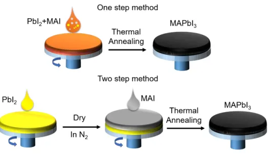
Figure 1.1 Crystal structure and chemical composition of organic-inorganic hybrid perovskite ... 2 Figure 1.2 Schematic representing one step and two step method in MAPBI3
perovskite film fabrication ... 3 Figure 2.1 Absorption spectra (a), PL spectra (b) and XRD patterns (c) of the
iodine perovskite films spun from solutions with a precursor ratio from 0.35 to 1. All the perovskite films in (a) and (b) were spun on PEDOT:PSS except the ones that are labeled as on ITO. The precursor ratio of the perovskite films spun on ITO
is 0.7. ... 9 Figure 2.2 Top view SEM images of the iodine perovskite films spun from
solutions with a precursor ratio from 0.35 to 1. The scale bars of SEM images are
2 𝜇𝑚 in the sample with a precursor ratio of 0.6 and 3 𝜇𝑚 for all others. ...11 Figure 2.3 (a) Tilted cross-section SEM image of a perovskite film spun from
solution with a precursor ratio of 0.78. The continuous perovskite layer (CPL) and the microstructure perovskite layer (MPL) are labeled. The scale bar is 1 mm; (b) the schematic device structure of the perovskite PV devices. The thickness of each
layer was not in scale with the real thickness for clarity. . ...12 Figure 2.4 The photocurrents of the devices under AM 1.5 simulated illumination
with different precursor ratios (a), different acceptor layers (b), and different thicknesses (c). The devices in (a) have a thickness of 140 nm and an ICBA acceptor layer; the devices in (b) have a precursor ratio of 0.6 and a thickness of 75 nm. The devices in (c) have a precursor ratio of 0.6 and an ICBA acceptor layer.
(d) The photo- and dark-currents of the highest efficiency device. ...14 Figure 2.5 Photocurrents of a high-performance perovskite device measured with
different delay between measurement points (a) and different sweep directions (b).
The photocurrent was tested under AM 1.5 simulated illumination. ...16 Figure 2.6 (a) Top view of the SEM image of the as-spun perovskite film. (b) Top
view SEM image of the perovskite film after ICBA spin-coating. The perovskite films in (a) and (b) were spun from the solution with a precursor ratio of 0.6 and a concentration of 250 mg/ml. The scale bar is 500 nm. (c) Cross-section SEM of a
working device with a thin (75 nm) perovskite layer ...18 Figure 2.7 Dark current of perovskite devices with different fullerene layer
fabrication processes. Black square, red circle, blue triangle curves are for the devices with a 50 nm C60, perovskite film washed by the DCB solvent, 20 nm spun
C60 plus 30 nm evaporated C60, respectively. ...19 Figure 2.8 Trap density of states (tDOS) for devices passivated by single PCBM
layer (blue triangles), single C60 layer (red dots), PCBM/C60 double fullerene layers
(grey stars); black squares represent the devices without fullerene passivation. ...21 Figure 3.1 (a) Schematic structure of the devices in this study. The thickness of
each layer was not in scale with the real thickness for clarity. (b) Cross-section scanning electron microscopy picture of perovskite on 1 wt% F4-TCNQ doped PTAA layer. SEM images of perovskite films on non-doped PTAA (c) and 1 wt%
Figure 3.2 (a) The photocurrents of the devices under AM 1.5 simulated illumination with different doping levels of PTAA layer. (b) Calculated and experimental fill factors of devices with different doping levels of HTL. External quantum efficiency (c) and steady maximum power output measurement (d) of the
best device. ...30 Figure 3.3 Series resistance of PTAA films with different F4-TCNQ doping levels.
The series resistance was measured by four probe method and slope of device I-V
curve ...32 Figure 3.4 Photocurrents of the devices with doped (a) or non-doped (b) HTL
under AM 1.5 simulated illumination. The HTL thickness was varied from 20 to 70 nm. (c) Corresponding series resistance of the doped or non-doped HTL films
derived from the slope of I-V curves. ...35 Figure 4.1 (a) The device structure of perovskite solar cells and (b) the energy
diagram that illustrates the principle of suppressing surface charge recombination by the insulating layer. The insulating layer suppresses charge recombination by separating the excess electrons and holes in the electron transport layer and perovskite layer, respectively; (c) A transmission electron microscopy cross-section image of a 19.6% efficiency device revealing the presence of 1-2 nm PS layer between perovskite and electron transport layer. The scale bar is 5 nm. The PS layer was made from commercial PS plastic foam, the picture of which was
also shown on the right. ...39 Figure 4.2 (a) Current density-voltage (J-V) characteristics of the devices with
different insulating tunneling contacts. The control device has 20 nm PCBM to replace the insulating layer; (b) The statistics of PCE distribution for perovskite
devices with PCBM (50 samples) and tunneling contact (50 samples) ...41 Figure 4.3 (a) J-V of the devices with PS layers of different thicknesses. (b)
Average EQE of 10 devices with a tunneling layer, and average EQE of 10 control devices with a PCBM contact layer. The EQE curves of the devices could be found in the supporting information; (c) Steady-state measurement of JSC and PCE for the best device with a PS tunneling layer. (d) Stability test of a perovskite device with PS tunneling layer. The legend in the figure represents the air exposure time
after the device was tested after being fabricated ...43 Figure 4.4 (a) Schematic diagram showing the cross-link process of fluoro-silane
layer on the perovskite film. (b) A picture of the perovskite device with fluoro-silane layer. The picture was taken after dipping the device in water for 1-2 min (c) A picture of the perovskite device without tunneling layer. The picture was taken after dipping the device in water for 5 seconds. (d) A picture showing the perovskite device with fluoro-silane layer had a 1.09 V photovoltage output in
water. ...45 Figure 4.5 c-AFM measurement of the local dark-current of the samples with the
structures of ITO/PTAA:F4-TCNQ/Perovskite (a), ITO/PTAA:F4-TCNQ/Perovskite/PS (b). c-AFM measurement of the local photocurrent of samples with the structure of ITO/PTAA:F4-TCNQ/Perovskite/C60 (c) and
Figure 4.6 Current-voltage (I-V) characteristics of electron-only device (a) and hole-only device (b). The insets of (a) and (b) show the structures of electron-only
and hole-only devices, respectively. ...49 Figure 4.7 Carrier recombination lifetime of perovskite devices with or without
PS tunneling layer measured by TPV. ...50 Figure 5.1 (a) Molecular structures of the sulfobetaine zwitterions used in this
study. (b) A photo of a CsPbI3 perovskite film with zwitterion. The zwitterion-stabilized CsPbI3 film had a black and mirror-like surface. (c) Absorption spectra of CsPbI3 perovskite films with or without NDSB201 zwitterion. (d) PL spectrum
of a CsPbI3 perovskite film with zwitterion. ...55 Figure 5.2 Cross-section SEM image of CsPbI3 films with (a) or without (b) SB
3-10 zwitterion. The scale bars of the images are 400 nm. (c) XRD patterns of the perovskite spun films fabricated by precursor solutions without (up) and with (bottom) SB 3-10 zwitterion. No thermal annealing was applied on the films and the spun films were measured immediately after fabrication. (d) FTIR measurement of SB 3-10 solution and SB 3-10 solutions mixed with different ratios of CsPbI3. The molar ratio of SB 3-10 to CsPbI3 was varied from 1:1 to 1:100. (e) Ultraviolet-visible spectroscopy measurement of the CsPbI3 solution and
CsPbI3 solutions mixed with different weight percentages of SB 3-10...57 Figure 5.3 Schematic representation of CsPbI3 crystal formation from precursor
solution without (a-c) or with (d-f) the zwitterion. PbI2 in the precursor solution coordinates with DMSO molecules to form crystallized PbI2∙DMSO colloids (a and d). Without the zwitterion, I- ions in the solution facilely coordinate to Pb2+ ions of the PbI2∙DMSO colloid to form corner-sharing 𝑃𝑏𝐼64 − octahedra and Cs+ ions occupy the octahedral sites (b), resulting in large-grained CsPbI3 film with orthorhombic phase (c). With zwitterion, the PbI2∙DMSO colloid size is deceased because zwitterions could interact with Cs+ and I- ions in the precursor solution. (e) The spun film before annealing shows amorphous phase. (f) The zwitterion molecules are expelled towards grain surface and grain boundaries during CsPbI3
grain growth, which maintain the small grains by impeding further grain growth. ...60 Figure 5.4 Selected region of FTIR spectra of SB3-10 powder and SB 3-10 mixed
with CsPbI3 powder. The SB 3-10 mixed with CsPbI3 powder was fabricated by mixing 1.5 wt% of SB 3-10 in CsPbI3 solution. Then the solution was spin-coated on glass substrates and thermally annealed at 100 ℃ for 20 min. After that the
films were scratched and the powder was collected for measurement. ...62 Figure 5.5 (a) Device structure of the cesium perovskite solar cells. (b) J-V curves
of the devices with different cesium perovskite layer thicknesses. NDSB201 was used to stabilize perovskite 𝛼-phase and the perovskite composition was CsPb(I0.98Cl0.02)3. (c) J-V curve of the champion CsPb(I0.98Cl0.02)3 device with perovskite layer treated by argon plasma. The perovskite layer thickness was 300 nm. (d) Steady-state measurement of photocurrent and PCE of the most efficient device. (e) EQE of the most efficient device. (f) The statistics of PCE distribution for CsPb(I0.98Cl0.02)3 devices with argon plasma treatment. (g) J-V curves of CsPb(I0.98Cl0.02)3 devices with perovskite layer annealed at 90 ℃ for 20 min and 12 hours. (h) PCE of a typical CsPb(I0.98Cl0.02)3 device kept in ambient environment as a function of storage time. The sample was kept in air without encapsulation
Figure 6.1 (a) Schematic Hall effect measurement setup and a typical Hall voltage test result. (b) Composition dependent carrier concentration (circle) and carrier mobility (square) in perovskite films formed by one-step pre-mixed precursor
deposition (black) and two-steps interdiffusion method (blue) ...70 Figure 6.2 (a) UPS spectra of the cut-off region and valence band edge region for
MAPbI3 films. Spectra a-e represent films deposited by different precursor ratios of 0.3, 0.65, 1.0, 1.7, and 0.3 precursor-ratio film tested after annealing at 150 C for 45 min, respectively. (b) UPS measured energetic levels of perovskite films formed by one-step method with different precursor ratios of 0.3, 0.65, 1.0, 1.7 (left four columns), and 0.3 precursor-ratio film after annealing at 150 C for 45 min (right column). EF, CB, and VB represent Fermi level, conductive band and valence band, respectively. The column colors of pink and blue represent the p-
and n-type, respectively. ...74 Figure 6.3 Schematic conductivity type conversions in perovskite films by excess
CH3NH3I (left side) or excess PbI2 (right side). Possible point defects in perovskite films caused by composition variation were illustrated correspondingly. The elemental defects in gray color are less-likely to form in the films, as discussed
in the manuscript. ...76 Figure 6.4 Photocurrent curves (a) and the corresponding VOC, JSC (b) of the
perovskite devices made by interdiffusion method. The perovskite films were made of spun 430 mg/ml PbI2 films, followed by MAI deposition with varied
LIST OF ABBREVIATIONS
BCP bathocuproine
C60 fullerene
CsPbI3 Cesium lead triiodide
perovskite
DMF N, N
-Dimethylmethanamide
DMSO dimethyl sulfoxide
DSSC dye-sensitized solar cells
ETL electron transporting layer
FA formamidinium
FAPbI3 formamidinium lead
triiodide
FF Fill factor
FTO Fluorine doped Tin Oxide
HTL hole transporting layer
ICBA indene-C60 bisadduct
I-V current-voltage
ITO indium tin oxide
J-V current density-voltage
JSC Short circuit current
MA methylammonium
MAPbI3 methylammonium lead
triiodide
MAPbBr3 methylammonium lead
OIHP organic-inorganic hybrid perovskites
PCBM [6,6]-phenyl-C61-butyric
acid methyl ester
PCE power conversion
efficiency
PEDOT:PSS
poly(3,4-ethylenedioxythiophene) polystyrene sulfonate
PTAA poly(triaryl amine)
PV photovoltaic
SEM scanning electron
microscopy
Si silicon
VOC Open circuit voltage
Chapter 1 Introduction to Organic-Inorganic Hybrid Perovskite ThinFilm Solar Cells
1.1History of perovskite solar cell
Organic-inorganic hybrid perovskites (OIHP) have been intensively studied as promising materials for next generation efficient, lightweight and low-cost thin filmsolar cells. As shown in Figure 1.1, the OIHP materials have a general crystal structure described as ABX3 perovskite structure, where A is methylammonium (MA+), formamidinium (FA+); B is lead (Pb2+), Tin (Sn2+) or germanium (Ge2+); X is halide (Cl-, Br- or I-). OIHP was for the first time used in solar cells in 2009 by Miyasaka et al as the dye in dye-sensitized solar cells (DSSCs).1 MAPbI3 and MAPbBr3 nanoparticles were distributed on mesoporous titanium oxide (TiO2) and a liquid electrolyte was used. A power conversion efficiency (PCE) of 3.8% was achieved. In 2011, Park et al. enhanced the efficiency of MAPbI3 solar cells to 6.5%.2 A crucial breakthrough made by Park et al. in 2012 was replacing the liquid electrolyte by solid-state hole transporting materials, where the first solid-state perovskite solar cell was fabricated and device PCE of 9.7% was reported.3 In 2013, Snaith et al. reported 10% efficiency in meso-superstructured solar cells where an insulating aluminum oxide (Al2O3) layer was covered on TiO2.4 In the Al2O3-based cells, the electrons must remain and transport in the perovskite until they are collected at the planar TiO2-coated FTO electrode, and hence indicating perovskite must be a good
deposition method, where PbI2 and CH3NH3I layers were sequentially deposited on TiO2
substrate.5 Snaith et al. reported a high efficiency of 15% in planar heterojunction structure solar cell where compact TiO2 layer was used.6 The efficiency of perovskite solar cell went up rapidly with certified PCE over 24% in 2019.
Figure 1.1 Crystal structure and chemical composition of organic-inorganic hybrid
perovskite
1.2perovskite film fabrication methods
Up to now, many methods have been developed for perovskite film fabrication, including vacuum and non-vacuum methods. Thermal evaporation is the most widely used vacuum based method which has demonstrated good perovskite device efficiency over 15%.6 Although perovskite films fabricated by thermal evaporation usually have good film uniformity and reproducibility, the concerns on the cost of this high-vacuum and high-temperature technique limit its industrial applications. Non-vacuum solution methods, such as spin coating and doctor blading, are simple and low-cost fabrications that are most widely used for perovskite film
Organic or cesium ions (MA, FA, Cs)
usually show higher device efficiency output and good reproducibility. Here I focused on the spin coating method for perovskite film fabrication which is good method for concept and performance demonstration in the research.
Figure 1.1 Schematic representing one step and two step method in MAPBI3 perovskite
film fabrication
There are primarily two ways in spin coating perovskite films, which are usually called one-step method and two-one-step method (Figure 1.2). In one-one-step approach, the perovskite precursor solution was prepared by mixing organic halide (MAI, FAI) and inorganic halide (e.g., PbI2) in dimethylformamide (DMF), dimethyl sulfoxide (DMSO) or their combination. The premixed precursor solution was spin-coated and annealed at around 100 ℃ to obtain perovskite
for the formation of MAPbI3 perovskite films in mesoporous structure solar cells, named as “sequential solution deposition”.5 This method was widely used in mesoporous structure, where the spun PbI2 film was dipped in MAI/IPA solution for MAPbI3 perovskite formation. When it was applied in planar structure device, the quick conversion of MAPbI3 perovskite could cause large film roughness and pinholes which results in large device leakage current. To solve this problem, two-step method was modified by spin-coating both PbI2 and MAI
layers successively on top flat substrate at very high spin speed. Although two step method increase the complexity of fabrication process, the perovskite film could be better manipulated by controlling the fabrication parameters in each step, enabling convenient control of film quality such as thickness, composition and grain size.
1.3Stability issues of perovskite material and solar cell
One of the biggest issues that hinder commercialization of perovskite solar cells is its stability problem. The most stable perovskite solar cell so far has operation stability around one year which is much shorter than the Si solar cells with typical stability longer than twenty years. Various works reported the degradation of perovskite material under external stimulus, such as moisture, thermal heat, oxygen and ultraviolet light.
1.3.1 Structure stability
t = rA+rX
√2∗(rB+rX) (1-1) where rA, rB, rX are ionic radius of ions in ABX3 structure. The ideal cubic structure has
tolerance factor of 1. Most perovskite materials satisfy 0.8 < t < 1 and non-perovskite structure will form when t is far from that range. MAPbI3 perovskite has a tetragonal structure with tolerance factor around 0.9.
Some perovskite materials, such as CsPbI3, could change to different crystal
structures/phases under different temperatures, which strongly determines electronic properties of the material. CsPbI3 has four structures at different temperatures.7 CsPbI3 shows orthorhombic structure (δ-phase) at room temperature. And it could transit to cubic perovskite structure (α -phase) when the temperature is higher than 310 ℃, which also reduces the film bandgap from over 2 eV for δ-phase to around 1.72 eV for α-phase. Upon cooling, the perovskite does not return to its original yellow phase immediately. Instead, it is first converted into the distorted black perovskite β-CsPbI3 (P4/mbm), γ-CsPbI3 (Pbnm), and then yellow δ-CsPbI3 at 260°C, 175°C and 25°C, respectively.7 The δ-phase consists of double-chains of non-corner-sharing Pb-I octahedra. In other three phases, they show corner-sharing Pb-Ioctahedra. δ-phase of CsPbI3 is also called yellow phase because its relatively large bandgap over 2 eV, while the other three phases are black phases with bandgap around 1.7 eV. Since only black phases of CsPbI3 are desired for photovoltaic application, stabilizing the black phase at room temperature becomes an important prerequisite for CsPbI3 solar cell fabrication.
1.3.2 Moisture stability
moisture easily to cause the degradation of OIHP materials. There have been many studies on the degradation process of MAPbI3 in humid air, where the degradation process of MAPbI3 films was well observed with the color change of the films from black to transparent. The de-coloring process is assigned to the formation of hydrated perovskites, such as MAPbI3∙H2O and
(MA)4PbI6·2H2O, which could further degrade to PbI2.8 The degradation observed in OIHP solar cells was frequently assigned to the intrinsically low moisture stability of OIHP materials and thus good device encapsulation is necessary for long-term device operation.
1.3.3 Thermal stability
Thermal stability is another challenging concern that affect the OIHP perovskite solar cell stability, because it is difficult to avoid the temperature increase during solar cell operation. Depending on the local conditions in the operation field (sunlight intensity, local temperature, wind speed, etc.), the real solar modules typically work at 30K-60 K higher than local
and cesium lead iodide (CsPbI3) perovskites which show significantly enhanced thermal
stability. Particularly, CsPbI3 perovskite is stable up to their melting points above 460 °C which is a promising material to improve the thermal stability of perovskite solar cells.
1.4Obstacles and future development
The OIHP solar cells have experienced a significant efficiency improvement from ~3% to over 24% in the past ten years. Substantial research efforts on fundamental study expanded our understanding about perovskite extraordinary electrical and optical properties. The development andsuccessful application of organic/inorganic charge transporting materials and passivation layer helped charge transfer at the interface and reduce charge recombination. Versatile OIHP layer fabrication methods have been invented, where perovskite film morphology is optimized including grain size, crystallinity and roughness. Benefiting from these efforts, the efficiency of perovskite solar cells in the lab scale has been increased significantly to over 24% in 2019.
However, OIHP photovoltaic still have great barriers before the final commercialization of this technique. The biggest problem comes withthe instability of perovskite materials, especially the most widely-used MAPbI3 which is sensitive to moisture, heat, UV light and oxygen. The efforts on device encapsulation, sealing layer inside device or composition optimization have been tried to solve the problem but more stability tests under harsh environments are suggested to meet the commercialization requirement. Large scale fabrication of perovskite module with high efficiency and low cost is another research interest before commercialization. The toxic effect of lead is also a potential problem for the perovskite solar cell commercialization, where replacing of lead by other metals is still challenging in obtaining high efficiency.
Chapter 2 Efficiency enhancement in perovskite solar cell by morphology engineering and defect passivation
This chapter studied the influence of the MAI/PbI2 precursor ratio on the perovskite film morphology and device performance. Using a non-stoichiometric precursor solution was demonstrated to be critical to form relatively continuous perovskite films. The compositions of the spun perovskite films were very sensitive to the surface of substrates, and can be very
different from that in precursor solutions. Remarkably, a unique double fullerene layers structure was adopted in the solar cell which could dramatically reduce dark current leakage by forming a Schottky junction with the anode, and effectively passivate traps in perovskite to increase fill factor to above 80%.
2.1 motivation
transport layer (TiO2) is used. But it causes serious problem in planar structure device, which leads to a large device leakage current as well as low fill factor (FF) and small open circuit voltage (VOC). To solve this problem, this chapter discuss the influence of the stoichiometric precursor ratio of the lead iodine/methylammonium halide solution on the perovskite film
morphology as well as the device performance. A non-stoichiometric precursor ratio was initially used by us which was found to be more suitable for perovskite formation to achieve a higher efficiency.
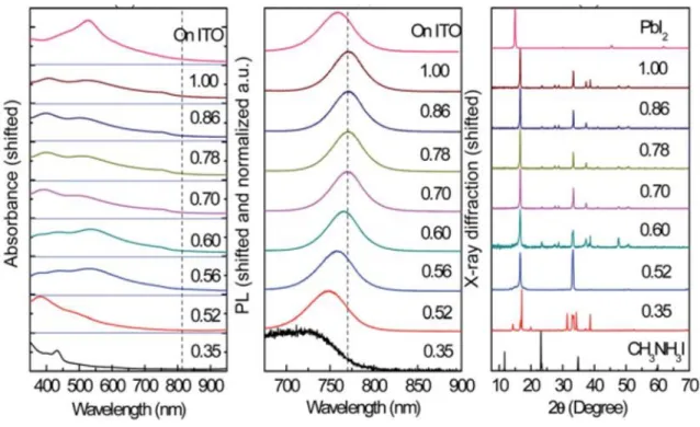
2.2 MAPbI3 film fabrication and characterization
Figure 2.1 Absorption spectra (a), PL spectra (b) and XRD patterns (c) of the iodine
perovskite films spun from solutions with a precursor ratio from 0.35 to 1. All the
as on ITO. The precursor ratio of the perovskite films spun on ITO is 0.7. (Reproduced by
permission of the Royal Society of Chemistry)
perovskite. Further increasing the PbI2 ratio over 0.7 does not change the absorption and PL spectrum shape or the peak intensity. The PL and absorption peaks of the film spun on ITO with the precursor ratio of 0.7 are close to those of the films on PEDOT:PSS with the precursor ratio of 0.56, indicating more PbI2 content in the film spun on PEDOT:PSS. It might ascribe to the better affinity of PbI2 to the amphiphilic PEDOT:PSS than that to ITO. XRD patterns in Figure 2.1 c reveal tetragonal perovskite forms with a small amount of PbI2 added in the precursor solution, while impurity peaks disappear when the precursor ratio is over 0.6. The non-unit precursor ratio for stoichiometric perovskite film formation indicates that the composition of the spun films is different from that in the precursor solution, which should attribute to the different affinities of MAI and PbI2 to the substrates.
Figure 2.2 Top view SEM images of the iodine perovskite films spun from solutions with
with a precursor ratio of 0.6 and 3 𝜇𝑚 for all others. (Reproduced by permission of the
Royal Society of Chemistry)
The top surface SEM images of perovskite films with different precursor ratios are shown in Figure 2.2. Increasing the amount of PbI2 in the films generally increases the film roughness, and a lot of microfibers are observed when the precursor ratio is larger than 0.8. The tiled cross-section and top-view SEM image of a perovskite film with a precursor ratio of 0.78 (Figure 2.3 a) showed distinct two-layer structures in the formed perovskite films: a flat, continuous bottom layer and a discontinuous top layer with many microstructures. The microstructures of the top layer vary dramatically with precursor ratios as shown in Figure 2.2. It is not yet clear why such two-layer structures form, but it is certainly related to the spin-coating process because the feature of the microstructures varies with different spin-coating parameters.
2.3 Device structure and performance
Figure 2.3 (a) Tilted cross-section SEM image of a perovskite film spun from solution with a
precursor ratio of 0.78. The continuous perovskite layer (CPL) and the microstructure
of the perovskite PV devices. The thickness of each layer was not in scale with the real thickness
for clarity. (Reproduced by permission of the Royal Society of Chemistry).
The typical device structure used to evaluate the formed perovskite films is shown in Figure 2.3 b. It is noted that a totally noncontinuous perovskite film is sketched for better illustration of the working mechanism of the devices in the follow-up discussion. It does not indicate that the perovskite film is that discontinuous because the size of the hole is enlarged for clarity. A double layer fullerene, with a spun PCBM or ICBA layer underneath followed by a thermal evaporated C60 layer, was used as the electron extraction layer. BCP is a well-known electron transport/hole blocking layer which has been widely used in organic light emitting diodes, organic
photodetectors and organic photovoltaic devices.10-13 Its functions have been thoroughly studied in OPVs including (1) blocking holes because of the poor hole mobility; (2) transporting
PCE. This observation provides a plausible explanation for the previously reported low efficiency PHJ perovskite solar cells by the solution process.
Figure 2.4 The photocurrents of the devices under AM 1.5 simulated illumination with different
precursor ratios (a), different acceptor layers (b), and different thicknesses (c). The devices in
(a) have a thickness of 140 nm and an ICBA acceptor layer; the devices in (b) have a precursor
ratio of 0.6 and a thickness of 75 nm. The devices in (c) have a precursor ratio of 0.6 and an
ICBA acceptor layer. (d) The photo- and dark-currents of the highest efficiency device.
Figure 2.4 b illustrates the photocurrent of devices with different spun fullerene or fullerene derivatives. It was found that the application of spun PCBM and ICBA significantly increases the VOC of the perovskite photovoltaic devices. The device fabrication parameters of the three devices studied here were controlled to be the same except for the fullerene layers. The VOC of the devices with perovskite coated by ICBA reaches 1.06 V which is 0.1–0.2 V larger than that of the device with PCBM interfacial modification, as shown in Table 2.1. The VOC enhancement in the devices with spun PCBM or ICBA can be explained by the Schottky junction formed between the spun fullerene films and the underneath PEDOT:PSS layer which is described below.
The FFs of the perovskite devices are sensitive to the composition and thickness of the perovskite layer as well as the electron extraction layers. The FF variation with the precursor ratio exhibits a peak value in the molar ratio of 0.6, as shown in Table 2.1. A thinner perovskite layer also gives a larger FF, most likely due to more efficient collection of charges and reduced recombination in the thinner perovskite films. The FFs are also comparable for the devices with PCBM and ICBA electron extraction layers, while a slightly larger FF of 80.1% is observed in the device with ICBA layers. This is in striking contrast to OPVs in which ICBA always yields a smaller FF than PCBM. To the best of our knowledge, the obtained FF is the highest among all the perovskite solar cells reported. The large FF and VOC in our bilayer structure devices with an ICBA layer indicate that the charge recombination limiting the efficiency in perovskite solar cells is different from that in OPVs or QDPVs.
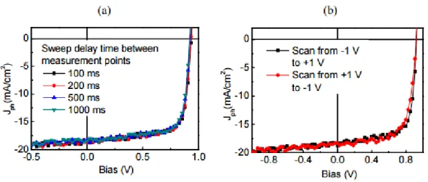
Figure 2.5 Photocurrents of a high-performance perovskite device measured with different
delay between measurement points (a) and different sweep directions (b). The photocurrent
was tested under AM 1.5 simulated illumination. (Reproduced by permission of the Royal
The optimized devices have a precursor ratio of 0.6, a thickness of 140 nm, and an ICBA acceptor layer. The thermal annealing time of the perovskite film was optimized to 60 minutes under 100 C. Meanwhile, perovskite/ICBA layers were annealed 30 minutes at the same
temperature. The highest efficiency device with photo- and dark-currents shown in Figure 2.4 d has a JSC of 15.7 mA/cm2, a VOC of 0.97 V, a FF of 80.1% and a PCE of 12.2%. It is expected that the slight annealing after ICBA coating drives the diffusion of ICBA into the perovskite for a larger contact area. No obvious hysteresis of photocurrent was observed in the high efficiency device by changing the voltage sweep rates or direction (Figure 2.5).
Figure 2.6 (a) Top view of the SEM image of the as-spun perovskite film. (b) Top view SEM
image of the perovskite film after ICBA spin-coating. The perovskite films in (a) and (b) were
spun from the solution with a precursor ratio of 0.6 and a concentration of 250 mg/ml. The scale
bar is 500 nm. (c) Cross-section SEM of a working device with a thin (75 nm) perovskite layer.
(Reproduced by permission of the Royal Society of Chemistry)
Device I: ITO/PEDOT:PSS/perovskite (140 nm)/C60 (50 nm, thermal-evaporated)/BCP/Al. Device II: ITO/PEDOT:PSS/perovskite (140 nm)/C60 (20 nm, spun)/C60 (30 nm, thermal evaporation)/BCP/Al.
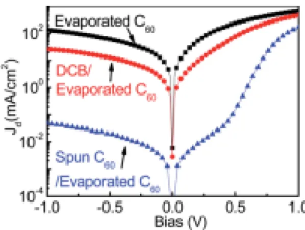
Figure 2.7 Dark current of perovskite devices with different fullerene layer fabrication
processes. Black square, red circle, blue triangle curves are for the devices with a 50 nm C60,
perovskite film washed by the DCB solvent, 20 nm spun C60 plus 30 nm evaporated C60,
respectively. (Reproduced by permission of the Royal Society of Chemistry)
Figure 2.7 shows the dark current curves of the devices with and without a spun C60 layer. The device without a spun C60 layer exhibits a huge leakage current density larger than 10 mA/cm2 even under a small reverse bias of 0.1 V. Nevertheless, after inserting a spun C60 layer onto the perovskite, the dark current is dramatically reduced by 3-4 orders of magnitude, demonstrating that a spun fullerene layer is crucial in preventing leakage. In order to find out whether the solvent of fullerene played a role in reducing leakage, we also made devices with DCB washed perovskites. No obvious morphological change of the perovskite film surface was observed in SEM images before and after DCB washing. Meanwhile, the dark current of the devices fabricated by DCB washed perovskite films still shows large leakage, although it was
reduced several times (Figure 2.7). As the DCB wash effect, though exists, is relatively minor, we then explained that the spun fullerene forms a conformal layer that cover most of the perovskite surface to prevent leakage.
The contact of fullerenes with PEDOT:PSS forms a Schottky junction, which was discovered by us previously.15 Consequently, the devices consist of two types of devices, perovskite/fullerene PHJ devices and PEDOT:PSS/fullerene Schottky junction devices, connected in parallel. This scenario is sketched in the device structure shown in Figure 2.3 b. The overall VOC is determined by both perovskite cell and the Schottky junction cell based on their relative cell area. The contact of PCBM and ICBA with PEDOT:PSS should not compromise the VOC of the whole devices because a large VOC of around 0.87 V and 0.95 V can be obtained from the
PCBM/PEDOT:PSS and ICBA/PEDOT:PSS Schottky junction devices.15 However, if C60 is spun onto perovskite, the device overall VOC was reduced to 0.5 V because the VOC of a C60/PEDOT:PSS Schottky junction is only around 0.45 V.
2.5 Defect passivation by fullerene layers
Figure 2.8 Trap density of states (tDOS) for devices passivated by single PCBM layer (blue
triangles), single C60 layer (red dots), PCBM/C60 double fullerene layers (grey stars); black
squares represent the devices without fullerene passivation. (Reproduced by permission of the Royal Society of Chemistry)
The other important role that this double fullerene layer structure plays is its better passivation effect of traps in perovskite. To verify this scenario, we conducted thermal
admittance spectroscopy (TAS) to quantitatively analyze the passivation of perovskite by PCBM and C60.16 TAS is a well-established technique for determination of the defect density of states which has been broadly applied in understanding defects in the thin film solar cells and organic solar cells.17 The trap density of states (tDOS) distribution can be derived from the angle frequency dependent capacitance via,
𝑁𝑇(𝐸𝜔) = −𝑉𝑏𝑖
𝑞𝑊 𝑑𝐶 𝑑𝜔
𝜔
𝑘𝑏𝑇 (2-1) where Vbi is the built-in potential, q is the element charge, W is the depletion width, C is
capacitance, 𝜔 is the applied angular frequency, kb is the Boltzmann's constant, and T is the temperature. Vbi and W are extracted from the capacitance-voltage measurement. The applied angular frequency 𝜔 defines the energy demarcation,
𝐸𝜔 = 𝑘𝑏𝑇𝑙𝑛 (𝜔0
𝜔) (2-2)
between 0.1 to 1000 kHz. The results in Figure 2.8 show that the devices without any fullerene layer have a relatively large trap density between 1017 and 1019 m3 eV-1 (black squares) which is detrimental to the device performance. Three trap bands can be identified as labeled in the figure (separated by red dotted lines). After depositing the C60 or PCBM layer, the tDOS reduced dramatically, indicating that both the C60 and PCBM effectively passivated the defects in perovskite films. It is noticed that C60 and PCBM have different but complementary passivation capability to the different trap bands. PCBM prefers to passivate the trap states in band 2 (0.40– 0.50 eV) and C60 has a stronger passivation effect on trap states with a trap depth larger than 0.50 eV (band 3). The tDOS of the device with PCBM and C60 double fullerene layers with an
optimum thermal annealing time is smaller than those with either PCBM or C60, and is about two orders of magnitude lower than the device without fullerenes in the whole defect spectral range. This result demonstrated that the PCBM and C60 cooperate with each other well and further reduce the trap densities. This explains the better device performance, especially the record FF, in our optimized devices with double fullerene layers.
2.6 Conclusion
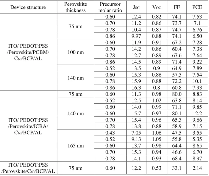
Table 2.1 Performance of devices with different precursor molar ratio, perovskite thicknesses and fullerene derivative layers. (Reproduced by permission of the Royal Society of Chemistry)
Device structure Perovskite thickness
Precursor
molar ratio JSC VOC FF PCE
ITO/ PEDOT:PSS /Perovskite/PCBM/
C60/BCP/AL
75 nm
0.60 12.4 0.82 74.1 7.53
0.70 11.2 0.86 73.7 7.1
0.78 10.4 0.87 74.7 6.76
0.86 9.97 0.88 74.1 6.50
100 nm
0.60 11.9 0.91 67.2 7.28
0.70 14.2 0.86 60.4 7.38
0.78 12.7 0.89 67.6 7.64
0.86 14.5 0.89 71.4 9.22
140 nm
0.52 13.5 0.9 64.9 7.89
0.60 15.3 0.86 57.3 7.54
0.78 15.9 0.88 72.2 10.1
0.86 16.3 0.8 60.8 7.93
ITO/ PEDOT:PSS /Perovskite/ICBA/
C60/BCP/AL
75 nm 0.60 11.3 0.98 80.0 8.83
140 nm
0.52 12.5 1.02 63.8 8.14
0.60 14.0 0.99 71.1 9.85
0.60 15.7 0.97 80.1 12.2
0.70 15.4 0.96 65.3 9.66
0.78 13.8 0.88 58.9 7.15
165 nm
0.43 7.05 1.06 47.5 3.55
0.52 9.13 1.05 55.8 5.35
0.60 13.7 0.98 64.4 8.65
0.70 15.3 0.94 46.6 6.70
0.78 14.1 0.93 68.4 8.97
ITO/ PEDOT:PSS
Chapter 3 efficiency enhancement in planar heterojunction organolead trihalide perovskite solar cells by a doped hole transport layer
In this chapter, the efficiency of a planar heterojunction MAPbI3 perovskite solar cell was further improved to 17.5% by using a doped polymer as hole transport layer. Doped poly(triaryl amine) (PTAA) by 2,3,5,6-Tetrafluoro-7,7,8,8-tetracyanoquinodimethane (F4-TCNQ) reduced device series resistance by three-folds, increasing the device fill factor to 74 %, open circuit voltage to 1.09 V without sacrificing the short circuit current. It reveals that the high resistivity of currently broadly applied polymer hole transport layer limits the device efficiency, and points a new direction to improve the device efficiency.
3.1 motivation
than 80 % and great promise to achieve higher power conversion efficiency, most of these PHJ OIPH devices still adopted PEDOT:PSS as HTL. However, the low work function of
PEDOT:PSS caused a relatively small VOC of around 0.90 V in these PHJ devices, compared to the typical VOC of >1.05 V in the inverted structure OIPH devices. Polymer HTMs are promising materials because of its sustainability to DMF wash, for example, poly[ N , N
′-bis(4-butylphenyl)- N , N ′- bis(phenyl)benzidine] (poly-TPD), was introduced into PHJ perovskite devices with device VOC greatly increased to 1.10 V. Meanwhile, another polymer HTM, PTAA, also showed great capability to increase device VOC and survive the DMF wash. However, the PCE of these polymer HTLs based OIPH devices was still around 15%. Compared with the best reported efficiency of PEDOT:PSS based perovskite devices, the higher VOC of polymer HTL based OIPH devices was obtained at the expense of a smaller FF. It was speculated that the higher resistivity of these polymer HTMs than PEDOT:PSS may hinder charge extraction efficiency which reduces FF of these devices. In this chapter, a highly efficient
solution-processed PHJ perovskite solar cells using 2,3,5,6-Tetrafluoro-7,7,8,8-tetracyanoquinodimethane (F4-TCNQ) doped PTAA as the HTL is discussed. F4-TCNQ doping was found to reduce the series resistance of the PTAA device by three times, which improved the device PCE, especially when thick HTL was used.
3.2 Experimental section
3.2.1 Device fabrication and characterization
4,4′,4′′-Tris[phenyl(m-tolyl)amino]triphenylamine (m-MTDATA) was mixed in the PTAA solution because the bare PTAA film was so smooth and non-wetting to DMF that PbI2 precursor was hardly spun on top of it. The perovskite films for device fabrication were made by interdiffusion method, in which PbI2 and MAI were sequentially spun on the substrates. The concentration of PbI2 was fixed at the 600 mg/ml and the concentration of MAI was varied from 50 mg/ml to 70 mg/ml. The spun films were annealed at 100 °C on hotplate under the cover of a glass petri dish. 10 µL - 30 µL of DMF solvent was added at the edge of the petri dish during annealing process. After that, [6,6]-phenyl-C61-butyric acid methyl ester (PCBM) (dissolved in DCB, 2 wt%) was spin coated on top of the perovskite layer at 6000 RPM for 35 s. The films were annealed at 100 °C for 60 min. Then 20 nm thickness of C60 was thermally evaporated with a deposition rate of 0.5 Å/s. The devices were finished by the evaporation of 7 nm 2,9-dimethyl-4,7-diphenyl-1,10-phenanthroline (BCP) and 100 nm thick aluminum electrode.
Generally, the procedures for making PTAA films in the resistivity measurement were same with that for device fabrication. But thicker PTAA layer of 200 nm was used for increasing the signal-noise ratio. The schematic diagram of setup and the method of measuring resistivity can be found elsewhere.22 The four probe measurement was conducted at atmosphere without encapsulation. Film thickness was measured by Bruker Dektak XTL step profiler. The
3.2.2 Fill factor Calculation
The method of calculating FF was based on assumption that the maximum power output of the solar cell approximately equals to the power in the absence of series resistance minus the power lose of the series resistance.23
𝐹𝐹 = 𝐹𝐹′∗ (1 − 𝑟) (3-1) where FF and 𝐹𝐹′ are the fill factor of devices with and without series resistance, respectively. r and ideal fill factor 𝐹𝐹′can be described by the following equations:23
𝑟 = 𝑅𝑆
𝑅′ (3-2) 𝑅′= 𝑉𝑀𝑃
𝐼𝑀𝑃 (3-3) 𝐼𝑀𝑃 = 𝐼𝐿− 𝐼0𝑒𝑥𝑝𝑞𝑉𝑀𝑃
𝑛𝑘𝑇 (3-4)
where RS is the series resistance. IMP andVMPare the maximum-power-point current and voltage of the device with negligible series resistance and infinitely large shunt resistance. IL is light
generated photocurrent, I0 is dark saturation current, q is elemental charge, n is ideal factor, k is
Boltzmann constant, T is temperature. Here, we assumed dark saturation current equals to 1*10 -16 mA/cm2. Series resistance can be calculated based not resistivity measured by four probe method and the device geometry. Assuming n equals to 1, IL equals to 24 mA/cm2 based on the
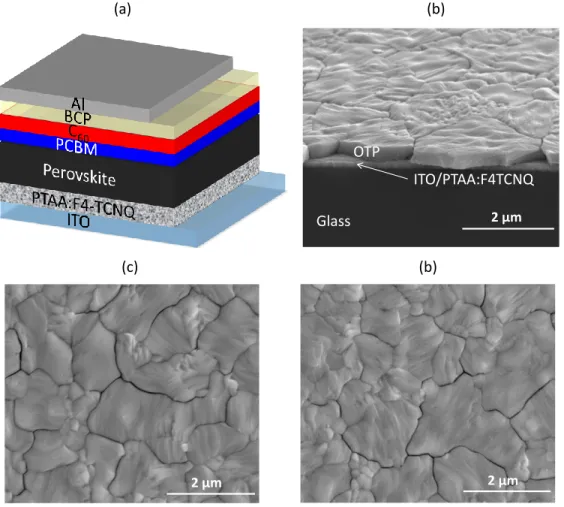
Figure 3.1 (a) Schematic structure of the devices in this study. The thickness of each layer was not
in scale with the real thickness for clarity. (b) Cross-section scanning electron microscopy picture of
perovskite on 1 wt% F4-TCNQ doped PTAA layer. SEM images of perovskite films on non-doped
PTAA (c) and 1 wt% F4-TCNQ doped PTAA (d).(Reproduced by permission of ELSEVIER)
Figure 3.1a shows the structure of the devices in this study. The perovskite films were made by interdiffusion method, where lead iodide (PbI2) and methylammonium iodide (MAI) were sequentially spun onto the substrates, followed by a thermal annealing driven diffusion process.24 It was discovered by us the surface of MAPbI3 can decompose during the thermal annealing process even though the annealing temperature was as low as 110 oC. MAI was found to
(a) (b)
2 μm Glass
OTP
ITO/PTAA:F4TCNQ
2 μm 2 μm
Figure 3.2 (a) The photocurrents of the devices under AM 1.5 simulated illumination with
different doping levels of PTAA layer. (b) Calculated and experimental fill factors of devices
with different doping levels of HTL. External quantum efficiency (c) and steady maximum
power output measurement (d) of the best device. (Reproduced by permission of ELSEVIER)
Figure 3.2a shows the current density-voltage (J-V) curves of devices with different F4-TCNQ doping concentration in the HTLs. The thickness of the HTL was kept unchanged by using a same solution concentration and spin rate. The changed doping level was found to have a significant impact on device performance, especially FF. As shown in the Figure 2b, the devices with 20 nm non-doped PTAA layer exhibited a low FF of 65%. After doping the PTAA layer by 1 wt% F4-TCNQ, the device FF was increased to 74%. Further increasing doping level to 10
0.0 0.3 0.6 0.9
-20 -16 -12 -8 -4 0 Jph (mA/cm 2 ) Bias (V) 0 wt% 0.01 wt% 0.1 wt% 1 wt% 2 wt% 10 wt% Doping ratio
300 450 600 750
0 20 40 60 80 100 EQE (%) Wavelength (nm) (a) (b) (c) (d)
0.000 0.01 0.1 1 10
55 60 65 70 75 80 Fill F actor (%)
Doping ratio (wt%) Measured
Calculated
0 10 20 30 40 50
-25 -20 -15 -10 -5 0 5 10 15 20 25 -25 -20 -15 -10 -5 0 5 10 15 20 25 PCE (%) Bias:0.85 V Current density:
20.6 mA/cm2
Jph
(mA/cm
2 )
Time (s)
PTAA showed the highest efficiency with a JSC of 21.6 mA/cm2, a VOC of 1.09 V, a FF of 74 % and PCE of 17.5 % under 1 sun illumination. Corresponding data can be found in Table 3-1. Figure 3.2c-d show the external quantum efficiency (EQE), steady photocurrent output and stabilized PCE of the device with 1 wt% F4-TCNQ dopant in the HTL. The calculated JSC of 21.0 mA/cm2 from EQE is in good agreement with that from J-V measurement. And the steady photocurrent measured at the maximum power point (0.85 V) is the same with that measured from J-V scanning, excluding the existence of obvious photocurrent hysteresis in our PHJ devices. The stabilized efficiency is 17.5%, confirming the accuracy of our device efficiency characterization. The absence of photocurrent hysteresis can be explained by the large grain grown on PTAA, and the application of double fullerene layer on the devices, which effectively reduce charge trap density at grain boundaries and film surface.29,30
3.4 Correlation between fill factor and resistivity
0.000
0.01
0.1
1
10
4
6
8
10
12
14
16
Doping ratio (wt%)
Seri
es resi
stance
(ohm*
cm
2
)
Figure 3.3 Series resistance of PTAA films with different F4-TCNQ doping levels. The series
resistance was measured by four probe method and slope of device I-V curve. (Reproduced by
permission of ELSEVIER)
Another possible reason is the electric field in J-V measurement is much larger than that in the four-probe measurement. In addition, the thickness of PTAA layer in devices was thin and may barely cover the whole substrate.
Now that we have demonstrated the doping effect of F4-TCNQ in changing the resistivity of the PTAA layer, the influence of resistance on device efficiency needs to be clarified. Here, we applied the equivalent circuit and simulation method in inorganic solar cell to calculate FFs. Details about the calculation can be found in the experimental section. The two curves in Figure 3.2b are the device FFs derived and J-V measured. The calculated FF variation is in good
0.0 0.2 0.4 0.6 0.8 1.0 -24 -20 -16 -12 -8 -4 0 4 J ph (mA/cm 2 ) Bias (V) 20 nm 40 nm 70 nm PTAA thickness (a) (b) (c)
0.0 0.2 0.4 0.6 0.8 1.0
-24 -20 -16 -12 -8 -4 0 4 J ph (mA/cm 2 ) Bias (V) 20 nm 40 nm 70 nm PTAA thickness
15 30 45 60 75
0 5 10 15 20 25 30
Figure 3.4Photocurrents of the devices with doped (a) or non-doped (b) HTL under AM 1.5
simulated illumination. The HTL thickness was varied from 20 to 70 nm. (c) Corresponding
series resistance of the doped or non-doped HTL films derived from the slope of I-V curves.
(Reproduced by permission of ELSEVIER)
Another merit for F4-TCNQ doping is that the reduced HTL resistance should make the device efficiency less dependent on HTL thickness. To demonstrate it, we compared the devices with doped or non-doped PTAA HTLs with different HTL thicknesses from 20 nm to 70 nm. Figure 3.4a-b show the J-V curves of devices with and without F4-TCNQ doping, respectively. Without doping, the device J-V curve gradually showed s-kink when the HTL thickness
increased to 70 nm. On the other hand, the devices with 1 wt% F4-TCNQ doped PTAA HTLs have PCE almost insensitive to PTAA film thickness. Figure 3.4c summarizes the series resistance of the devices with non-doped and doped PTAA of different thicknesses. For the devices containing 20 nm HTL, 1 wt% F4-TCNQ doping reduced the series resistance from 8.8 𝛺*cm2 to 6.2 𝛺*cm2. Lower series resistance was observed in the doped device, especially when the HTL is thick. The resistivity of the device with 70 nm HTL was reduced three times from 26.6𝛺*cm2 to 9.33𝛺*cm2 after doping with 1 wt% F4-TCNQ. The insensitivity of device PCE on HTL thickness is benefit for device reproducibility and especially attractive for large-area device fabrication.
3.5 Conclusion
the PCE of OIHP solar cells and pointed out a direction of further increasing the efficiency of OIHP PHJ solar cells to above 20% by exploring better dopants.
Table 3-1 Perovskite device performance with different F4-TCNQ doping levels in PTAA layers. RS is device series resistances derived from I-V curves and RS′ is series resistances of PTAA films derived from four-probe method. (Reproduced by permission of ELSEVIER)
Doping ratio
JSC
(mA/cm2)
VOC (V) FF (%) PCE (%) RS (Ω*cm2) R′S(Ω*cm2)
0 wt% 21.6 1.05 65.7 14.8 9.07 12.9
0.01 wt% 21.0 1.05 65.8 14.5 7.57 12.1
0.1 wt% 21.5 1.05 65.5 14.8 7.72 10.6
1 wt% 21.6 1.09 74.0 17.5 6.07 8.4
2 wt% 21.0 1.09 68.2 15.6 8.56 8.2
Chapter 4 Thin Insulating Tunneling Contacts for Efficient and Water-Resistant Perovskite Solar Cells
In this chapter, an insulating tunneling layer inserted between the perovskite and the electron collection layer in perovskite solar cells can reduce charge recombination, which was inspired by the success of applying tunneling contacts in silicon solar cells. Many insulating polymers, including commercial plastic foam which is broadly used for packaging, can form a tunneling contact at the cathode side. The tunneling contact allows the transport of electrons from
perovskite to cathode, while block holes into the perovskite layer. Devices with these insulating materials exhibited an increased PCE of 20.3 % under one sun illumination. This simple non-lattice-matching structure enables the capping of the perovskite films by super-hydrophobic insulating layers, which dramatically enhances resistance of perovskite solar cells to water-caused damage without further encapsulation.
4.1 Motivation
The efficiency of OIHP solar cells has rocketed in the last few years, which has been
crystallinity of the perovskite films with recent rapid improvement in material morphology controlling.26,39-44 The enlargement of grains also significantly reduces carrier recombination at perovskite grain boundaries (GBs), which is facilitated by the advance of passivation techniques to further reduce recombination at GBs and film surface.45-47 Now that the photo-generated carriers can flow through perovskite films with negligible charge recombination, minimizing the charge recombination at the contacts becomes increasingly important to achieve highly efficient perovskite solar cells.
The tunneling junctions applied in silicon solar cells, which resulted in the most efficient silicon solar panels in the world, are comprised of an insulating oxide or a thin-layer of
amorphous silicon (HIT structure) inserted between the intrinsic silicon and the heavily-doped silicon layer or indium-tin-oxide (ITO) layer. The tunneling junctions have been shown to suppress the charge recombination at contacts and passivate the surface to increase device efficiency.48,49 The inserted insulating layer can selectively conduct one type of charges while block the other type, which spatially separates photo-generated electrons and holes to reduce their recombination, because the charge selection electrodes or charge transport layers have energy-matching electronic states for one type of charges to tunnel into but not for the other type. The success of HIT structure in silicon solar cells inspired us to use insulating contacts in
4.2 Efficiency enhancement by tunneling contacts
Figure 4.1 (a) The device structure of perovskite solar cells and (b) the energy diagram that
illustrates the principle of suppressing surface charge recombination by the insulating layer. The
insulating layer suppresses charge recombination by separating the excess electrons and holes in
the electron transport layer and perovskite layer, respectively; (c) A transmission electron
microscopy cross-section image of a 19.6% efficiency device revealing the presence of 1-2 nm PS
C
60/B C P
P S
P erovskite
(a)
(b)
C
60
HOMO 6.2 eV
LUMO 4.5 eV
DOS
Perovskite
CBM 3.9 eV
VBM 5.4 eV
Electron
Hole
-+
Electron
density
Hole
density
layer between perovskite and electron transport layer. The scale bar is 5 nm. The PS layer was
made from commercial PS plastic foam, the picture of which was also shown on the right.
(Reproduced by permission of WILEY)
Figure 4.1ashows the structure of the devices in this study where the tunneling junction locates at the cathode side. An insulating polymer is inserted between the perovskite and the electron collecting fullerene (C60) layers, and the proposed energy diagram in Figure 4.1b is also shown to illustrate the function of insulating layer in transporting electrons and blocking holes in the perovskite layer. Photo-generated electrons at conduction band minimal (CBM) of the
perovskite layer can tunnel to the excited electronic states in C60, followed by their relaxation to the lowest unoccupied molecular orbital (LUMO) of C60, because there are energy-matching unoccupied states in C60 for electrons to tunneling into. On the contrary, these is no energy-matching state in C60 which could allow the holes to tunnel into. Therefore, the tunneling rate of holes from perovskite to C60 will be very low. The thin insulating layer thus allows the transport of generated electrons in perovskite to C60 layer by tunneling, and also blocks the photo-generated holes back into the perovskite layer. Therefore, the insulating tunneling layer causes a spatial separation of the photo-generated electrons and holes, which reduces their recombination at the contact of the perovskite and electron transport layers.
tunneling materials in this study. The insulating polymers spun on the perovskite films could form a conformal tunneling layer, as verified by the high resolution transmission electron microscopy (TEM) cross-section image of the devices. As shown in Figure 4.1c, the spun PS layer with a thickness of 1-2 nm conformably covers the perovskite layer.
Figure 4.2 (a) Current density-voltage (J-V) characteristics of the devices with different
insulating tunneling contacts. The control device has 20 nm PCBM to replace the insulating
layer; (b) The statistics of PCE distribution for perovskite devices with PCBM (50 samples) and
tunneling contact (50 samples). (Reproduced by permission of WILEY)
Figure 4.2a shows the photocurrent curves of perovskite devices with different insulating polymers inserted and that of the control device with 20 nm PCBM to replace the insulating polymer layer. The control device has a short circuit current density (JSC) of 21.1 mA/cm2, an open circuit voltage (VOC) of 1.07 V, a fill factor (FF) of 74.9 %, and a PCE of 16.9 %, which represent a typical performance of PCBM passivated perovskite devices.50 In a striking contrast, the devices with polymer tunneling contacts exhibited an increased JSC and FF. The devices with PS, PVDF-TrFE and Teflon tunneling layer showed higher JSC of 22.9 mA/cm2, 22.9 mA/cm2
0.0 0.3 0.6 0.9 -24 -20 -16 -12 -8 -4 0 4 J ph (m A/cm 2 ) Bias (V) 0.02% PS 0.1% PS 0.5% PS 1.0% PS 2.0% PS
Tunneling layer thickness
0 50 100 150 200 -25 -20 -15 -10 -5 0 5 10 15 20 25 PCE (%) Current density: 21.5 (mA/cm2) Jph
(m
A/cm
2 )
Time (s)
PCE: 20.3 % Bias @ 0.94 V
(a)
(b)
(c)
(d)
0.0 0.3 0.6 0.9 -24 -20 -16 -12 -8 -4 0 4 Tunneling layers J ph (m A/cm 2 ) Bias (V) PS PVDF-TrFE Teflon
PS plastic foam Fluoro silane Control:PCBM
400 500 600 700 800
0 20 40 60 80 100 EQE (%) PS Control: PCBM Wavelength (nm)
12 14 16 18 20 0 5 10 15 20 PCBM contact Tunneling contact Coun ts PCE (%)
0.0 0.3 0.6 0.9 -24 -20 -16 -12 -8 -4 0 4 24 Hours 48 Hours 72 Hours 120 Hours Curre
nt Density (mA/cm
2 )
and 22.8 mA/cm2, respectively. Meanwhile, the FFs for devices with inserted PS, PVDF-TrFE and Teflon tunneling contacts were also increased to 79.6 %, 77.6 % and 75.6 %, respectively. The performances of perovskite devices with different tunneling layers were also summarized in Table 4-1. It should be mentioned that the VOC of the perovskite devices with tunneling contacts fabricated from different batches slightly varied between 1.05 V to 1.11 V. Statistic VOC
distributions of 50 samples indicate that the devices with tunneling contacts have a higher average VOC of 1.07 V, compared with 1.05 V of the control devices. The statistics of PCE in Figure 4.2b, demonstrate the reliability and the repeatability of the performance enhancement by the tunneling contacts. The universal performance enhancement by different insulating polymers and no change of trap density measured by thermal admittance spectroscopy belittle the
Figure 4.3 (a) J-V of the devices with PS layers of different thicknesses. (b) Average EQE of 10
devices with a tunneling layer, and average EQE of 10 control devices with a PCBM contact
layer. The EQE curves of the devices could be found in the supporting information; (c)
Steady-state measurement of JSC and PCE for the best device with a PS tunneling layer. (d) Stability
test of a perovskite device with PS tunneling layer. The legend in the figure represents the air
exposure time after the device was tested after being fabricated. (Reproduced by permission of
WILEY)
Since the tunneling probability strongly depends on tunneling-layer thickness, the thickness of the tunneling layer should significantly influence the electron extraction efficiency and thus device efficiency.51,52 Figure 4.3a shows the photocurrent curves of perovskite devices with PS
0.0 0.3 0.6 0.9 -24 -20 -16 -12 -8 -4 0 4 Jph (m A/cm 2 ) Bias (V) 0.02% PS 0.1% PS 0.5% PS 1.0% PS 2.0% PS
Tunneling layer thickness
0 50 100 150 200 -25 -20 -15 -10 -5 0 5 10 15 20 25 PCE (%) Current density: 21.5 (mA/cm2) Jph
(m
A/cm
2 )
Time (s)
PCE: 20.3 % Bias @ 0.94 V
(a) (b)
(c) (d)
0.0 0.3 0.6 0.9 -24 -20 -16 -12 -8 -4 0 4 Tunneling layers Jph (m A/cm 2 ) Bias (V) PS PVDF-TrFE Teflon
PS plastic foam Fluoro silane Control:PCBM
400 500 600 700 800
0 20 40 60 80 100 EQE (%) PS Control: PCBM Wavelength (nm)
12 14 16 18 20 0 5 10 15 20 PCBM contact Tunneling contact Coun ts PCE (%)
0.0 0.3 0.6 0.9 -24 -20 -16 -12 -8 -4 0 4 24 Hours 48 Hours 72 Hours 120 Hours Curre
nt Density (mA/cm
layers of different thicknesses which were tuned by varying the concentration of PS solution in the spin-coating process. As shown in Figure 4.3a, for PS solution with a concentration of 0.02 %, the device showed a JSC of 20.8 mA/cm2, a VOC of 1.05 V, a FF of 75.1 % and a PCE of 16.4 %, which is comparable to that of the PCBM-passivated devices. This can be explained by the fact that the PS layer formed from the solution with such low PS concentration is barely continuous, and thus the device resembles the control device without PS layer. When the PS concentration was increased to 0.1 %, 0.5 % and 1.0 %, the photocurrents were significantly increased to 22.0 mA/cm2, 22.8 mA/cm2 and 22.9 mA/cm2, respectively. The best devices were made by 1.0 % PS solution, exhibiting a VOC of 1.10 V, a JSC of 22.9 mA/cm2, a FF of 80.6 % and a PCE of 20.3 % from the photocurrent scanning. For these devices, the PS layer thickness was estimated to be 1-2 nm from the high resolution TEM shown in Figure 4.1b. Further
increasing PS layer thickness severely reduced the JSC, VOC, and FF to 20.0 mA/cm2, 1.03 V and 49.0 %, respectively, because the increased tunneling layer thickness reduced electron tunneling rate. Figure 4.3b show the average external quantum efficiency (EQE) spectrum of devices with PS and PCBM as the contact layer. Figure 4.3c shows the steady photocurrent and PCE
4.3 Increasing air and water stability by insulating contacts
Figure 4.4 (a) Schematic diagram showing the cross-link process of fluoro-silane layer on the
perovskite film. (b) A picture of the perovskite device with fluoro-silane layer. The picture was
taken after dipping the device in water for 1-2 min (c) A picture of the perovskite device without
tunneling layer. The picture was taken after dipping the device in water for 5 seconds. (d) A picture
showing the perovskite device with fluoro-silane layer had a 1.09 V photovoltage output in water.
(Reproduced by permission of WILEY)
The insulating polymer may serve as a water-resistant layer to protect the perovskite film from water damage. The speculation stemmed from the observation that the perovskite devices with insulating polymers generally showed a better stability in air (Figure 4.3d ), while the control devices without insulating polymers always degraded to yellow color in several days.53
(a)
(b)
Device with fluoro silane contact
Device with hydrophobic contact
Device with PCBM contact
In water In water
H20
Spin coat Cross-link
HCl H
20
To confirm it, we chose a hydrophobic insulating fluoro-silane,