Abstract-- This paper presents an original modular plug-in type assembly approach for a single phase-inverter. The main focus here is, indicatively, on the power range 1-20 kW, but the methodology can be transferred to higher power levels, too. At the core of the inverter lies a power-dense double-sided-cooled half-bridge power switch architecture with integrated cooler, which is interconnected to filter elements, gate-driver and control circuitry by means of compact flat connectors. The integration exercise targets, on the one hand, the optimization of the power switch performance and reliability, as well as the reduction of circuit parasitic elements; on the other, the production of a system compatible with maintenance and repairing, featuring minimized impact of single component failure on the system maintenance and repair cost and thus on its availability. Preliminary experimental tests demonstrate the nominal functionality of the inverter.
Index Terms—Integrated circuit packaging; inverters; reliability; electro-thermal effects; electro-magnetic interference.
I. INTRODUCTION
Efficiency, power density and reliability are the main figures of merit which have traditionally driven power electronics technology evolution. Recently, emphasis has also been put more and more on manufacturability and modularity as key enablers of competitive product development. In view of the conflicting requirements typically underlying the optimization of these characteristics of a power system, their conjunct optimization proves a challenging undertaking, which requires consideration of all main components of a converter: solid-state devices, thermal management, passive filter elements and auxiliary circuitry used for control, driving and protection. Fig. 1 schematically illustrates the breakdown of a single-phase inverter into its main functional parts. This work proposes an exercise of overall re-consideration and comprehensive optimization of the way the inverter is put together. The main focus being on the optimization of performance, reliability and power density, manufacturing, assembly and maintenance aspects are also duly taken into account to deliver a novel approach at system level integration.
Past examples of advanced inverter integration and assembly have delivered significant progress beyond state-of-the-art as far as packaging, layout, cooling and interconnection solutions are concerned [1-4]. In particular, [1, 2] focused on fully bond-wireless power modules with double sided cooling and demonstrated a 30% higher power density capability in the development of a railway traction inverter with the same reliability figures as with conventional assembly using commercial power modules. [3] progressed the ideas presented
in [1-2] by simplifying the assembly process and reducing the number of manufacturing steps and interfaces and addressing the integration of a functional switch (i.e., a half-bridge structure), as opposed to the integration of a single switch with free-wheeling diode: this was demonstrated to be beneficial to the device switching performance and to the electro-magnetic interference (EMI) signature of the system. Also, [2] has the merit of fully decoupling the drive and power current paths and of using embedded flat terminals for external interconnections. Both [1-2] and [3] targeted, however, the comprehensive integration of the inverter system within a unique block and did not devise credible solutions to bring along reduced system impact by single component failure, nor to enhance the repairable nature of the system to yield improved availability. Also, much of the benefits of the proposed integration exercise at power switch level are lost in the system level assembly, due to relative lack of advancement in the design of suitable connectors. Other noteworthy examples of comprehensive system level integration have been produced, which however, address different power ranges and application domains, relying on technologies which would not be applicable and transferable in a straightforward manner to higher power (and, in particular, higher voltage) levels due to both very challenging technological needs associated with the high integration level and with quite high manufacturing costs [4]. Also, since such solutions do not cater for the ability to intervene on the system and repair it, they are not-viable for a number of applications, ranging from transport to renewable energies. Finally, a number of packaging and integration exercises have targeted the production of high-temperature capable solutions, specifically in relation to the use of wide-band-gap (WBG) power devices [5].
In this work, the novelty is threefold:
- the integration of the power switches is further enhanced by adopting flip-chip type device mounting and by introducing the use of vertical vias and embedded parallel current conduction layers, which benefit both the electro-magnetic and the electro-thermal performance of the semiconductor devices;
- protruding embedded flat contact terminals and bespoke connectors are used to ensure the low parasitic inductance nature of the design is preserved when moving from the switch to the system level;
Modular assembly of a single-phase inverter
based on integrated functional blocks
- packaging bases on the identification of functional blocks within the inverter structure and the integration exercise correspondingly addresses, first, the optimization of each block individually, then, the optimization of their interconnection.
The result is a solution which preserves all of the positive features of [1-3] and which enhances the state-of-the-art with better performing power switches, reduced assembly and repair costs, improved availability of the system.
[image:2.612.336.533.366.558.2]The design follows a built-in reliability approach, consisting in the minimization of the electro-thermal and electro-thermal stresses on the device, which, at the same time, benefits the inverter efficiency. These considerations include both the manufacturing process (reduction of residual stresses) and the actual mission and load profile of the inverter. At the center is a very compact high-performance half-bridge power switch concept (HBS in Fig. 1), which makes use of a number of advanced features in both device and substrate manufacturing to deliver a fully bond-wire-less, double-sided-cooled, low profile high-frequency capable switching element. The design of the power switch is tightly coupled with that of its cooler to deliver a solution, which progresses beyond state-of-the-art in performance and reliability, by enabling very effective cooling while reducing significantly the number of interfaces and eliminating altogether the use of wire-bonds. The switch is interconnected to the rest of the system by means of custom designed connectors, which also serve the function of packaging for a number of components, while ensuring that the enhanced features implemented at switch level are not lost in the interconnection to the additional components of the inverter.
Fig.1 Schematic diagram of the open-loop inverter, with identification of its main functional parts.
The exercise presented here has future developments centered on wide-band-gap semiconductor device technologies in its field of sight, particularly as far as the need for higher switching frequencies and higher operating temperatures are concerned.
II.POWER SWITCH
A. Module
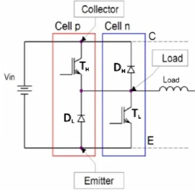
Fig. 2 shows a basic schematic of a half-bridge type switch, implemented with diodes and IGBTs in this case.
In switching applications supplying inductive loads, the load current is commutated at high-frequency between the devices in either the leg referred to as positive (p) cell or the leg referred
to as negative (n) cell: the terminology to denote the switching cells is derived from inverter current polarity, but similar considerations apply to the case of dc-dc converters, depending on the direction of power transfer [6]. So, from an application point of view, to minimize parasitic inductance and optimize switching performance, the ideal layout and packaging scheme of a half-bridge type switch should target the integration of the transistor in the high-side switch (TH) with the diode in the low-side switch (DL), and, vice-versa, the integration of the transistor in the low-side switch with the diode in the high-side switch (TL-DH).
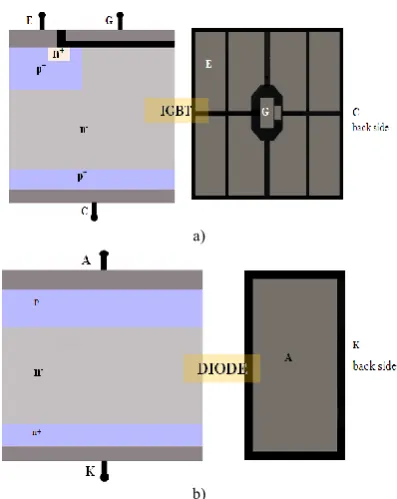
[image:2.612.47.300.432.532.2]Here, the switch is implemented in an innovative sandwich type assembly, where each IGBT-diode pair is soldered back-side down on separate substrates [7]: as compared with previously proposed approaches (see [8], for example), this arrangement offers the possibility to keep the interconnection loops and the corresponding stray inductance between TH-DL and between TL-DH at a minimum, while ensuring that all devices can be efficiently cooled via their preferential heat-transfer path, that is the backside. This way, while double sided cooling is still achieved, the thermal performance of the assembly is fully symmetrical. The devices used in this work are shown in Fig. 3: they are 70μm thin IGBTs and diodes rated at 600 V/ 200A, with lateral dimensionsof10mm x 9.5mm and 9.5mm x 5.5mm for IGBT and diode, respectively.
Fig.2 Schematic diagram of a half-bridge switch connected to an inductive load, with indication of p- and n-Cells to be integrated for optimum switching performance.
a)
[image:3.612.73.272.45.295.2]b)
Fig 3. Schematic cross-sectionand actual structure of IGBT, a), diode, b), chips. E, G and C indicate the IGBT Emitter, Gate and Collector terminals; A and K indicate the diode Anode and Cathode terminals.
The integration relies on advanced ceramic substrate technology, featuring double-etched patterned copper tracks for bond-wire-less interconnection and packaging; filled vias are also used in the ceramic substrates for vertical current conduction, which enables the introduction of a ground-plane structure within the switch, with greatly reduced overall values of parasitic inductance; finally, protruding broad and flat contacts derived from the substrate tracks themselves are used for interconnection to the rest of the system (filters, load and gate-drivers). With relevance to the circuit schematic of Fig. 2, the switch integration concept is illustrated in Fig. 4. It comprises of two ceramic substrates, with devices soldered back-side down pairwise onto them. To connect the chips top metallization, double-etching of the tracks on the ceramic substrates is used, which creates interconnection posts of suitable dimensions even for the smaller gate terminal. This solution allows for the use of a single solder layer between device metallization and copper post, enabling very compact and thin assembly when the two substrates are interconnected to form a sandwich type structure. As also indicated in Fig. 4, vias in the ceramic substrates are used for interconnection to a ground plane (denoted by the terminal E), which enables minimization of stray inductance. The intermediate ground plane is achieved by actually pressing together two ceramics substrates into a multi-layer single one. In this design, the power and drive terminals are on opposite sides of the switch and are both implemented with high-frequency compatible terminals, also integrated within the substrate design.
A cross-sectional view of the resulting final assembly, with the top substrate connected onto the bottom one, is shown in Fig. 5, with a detail of each component dimensions.The copper tracks are colored orange, the ceramic in dark grey, while the
lighter grey layers indicate tin-silver (Sn-3.5Ag) solder layers with 100 μm thickness. The IGBT chip is colored green.
[image:3.612.316.555.82.240.2]Fig. 4. Schematic 3D finite element structural model with detail of topical features.
Fig. 5. Vertical cross section (at the TL IGBT) of the proposed integrated power
switch. All dimensions are in mm.
This concept represents a significant incremental development on recently proposed solutions, from both a manufacturing and an application perspective [9].
B. Manufacturing
The devised solution is compatible with both sintering and soldering technologies, which can be applied according to the needs and aims of the hardware development. Whereas soldering proved sufficient for the prototype presented here, to cope with the reduced feature sizes of upcoming WBG power device technologies, it is expected that sintering will yield better control of resulting interface layers and their quality. Also, sintering becomes a necessity when higher temperature operation electronics is in focus. The devices require bespoke finishing independent of what joining solution is applied. The finished chosen in this case, as described above, ensures compatibility with both processes. The quality of the finish clearly plays a major role in the final reliability of the assembly: most device manufacturers do now cater for solder-able device finish of high quality and the possibility for procurement of suitably finished semiconductor chips is certainly open, depending mainly on purchase quantities.
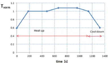
[image:3.612.321.556.277.372.2]operation of the switches [9]. In this case, that is particularly important in view of the double substrate used in the bottom part of the switch and the asymmetry in the volume and weight distribution of the substrates. So, it is extremely important to carefully select the thickness and shape of all materials involved in the assembly to ensure satisfactory results. To that aim, power switch design also needs to encompass a phase of parametric thermo-mechanical simulations aimed at delivering optimum structural design choices (e.g., ceramic and copper tracks thicknesses; relative thickness of tracks on different substrates and sides of the ceramic) for a given set of assembly process parameters (e.g., reflow profile). Fig. 6 shows the normalized solder reflow temperature profile used in our laboratory to manufacture the switch. Fig. 7 shows the substrate displacement at the time of maximum warpage during the reflow temperature cycle for both the top (a) and bottom (b) substrates when optimized values of ceramic and copper track thicknesses have been chosen, indicating contained values that enable proper assembly process.
Fig. 6. Reflow temperature profile for switch assembly.
a) b)
Fig. 7. Results of thermo-mechanical simulations indicating contained maximum warpage values during the assembly solder reflow process with optimized structural design choices for ceramic and copper tracks thicknesses. The scale unit is cm.
Extensive thermo-mechanical studies of the switch assembly have been carried out also for representative mission profiles, confirming the design and validating the technology options in terms of longer-term degradation and reliability.
In view of the results obtained in the design phase on the thermo-mechanical performance, the prototype was constructed using silicon-nitride (Si3N4) ceramic substrates. A photograph of the devices and of the double-etched substrates is shown in Fig. 8; Fig. 9 shows the fully assembled switch with the protruding electrical contacts for interconnection to gate drivers, load inductor and input filter. The assembly was
successful, with no evidence of any residual stresses in the switch.
[image:4.612.350.531.281.416.2]Fig. 8. Open view with detail of the double-etched posts (shaded areas). Here, the vias are not visible since they are filled with copper and plated.
Fig. 9. Fully integrated half-bridge switch (HBS) featuring complete separation of power and driving loops.
[image:4.612.76.267.295.406.2] [image:4.612.51.278.435.537.2]Fig. 10. Detail of switch filling for dielectric isolation and environmental insulation.
C. Electromagnetic analysis
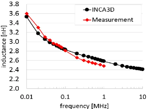
[image:5.612.320.559.51.229.2]From an electro-magnetic point of view, the design enables to: minimize the stray inductance associated with the drive loop (terminals GH-EH and GL-EL, indicating the high side and low-side gate and emitter contacts, respectively); to keep the drive and power loops fully separated, so that fast switch current variations do not interfere with the driving action as a result of the stray inductance [10]; finally, by means of the conducting vias created in the ceramic substrate, to implement a tight three-planes current conduction assembly (terminals C, Load and E) with largely overlapping conductors and an effective ground-plane covering the whole surface of the bottom metallization. The overall switch loop inductance can be thus greatly contained. The stray inductance of the power loop is important because it is mainly responsible of the over-voltages on the IGBTs at turn-off. Electromagnetic simulations have been done to evaluate the power loop stray inductance of our layout, followed by experimental validation. INCA3D, a software based on the PEEC (Partial Element Equivalent Circuit) method was used for the simulation [11]. With the PEEC method it is possible to extract the electric parameters as resistance, self and mutual inductance, from the geometry of the electric conductors of a circuit. The analysis, made with the software package INCA3D [12], was carried out varying the frequency of the test current applied to the power loop. We chose to mesh the 3D domain adapting it with the frequency of the sinusoidal current applied (automatically done by the software). We considered a switching frequency of 10 kHz, then frequency analysis has been done starting from this frequency up the harmonic at 10 MHz. The result of this parametric simulation is shown in Fig. 11. Ls varies from around 3.5 nH at 10 kHz, to 2.4 nH at 10 MHz. To validate the results of computer aided design, a measurement of a power switch module was carried out. This was done using an LCR meter HP 4284A and its test fixture. Biasing the loop with a maximum amplitude current of around 2 mA, we obtained 3.6 nH and 2.5 nH, at 1 kHz and 1 MHz respectively. The match between simulation and measurement is good.
Fig. 11. Simulated and measured power loop stray inductance.
[image:5.612.72.271.52.162.2]The stray inductance in the gate-source drive loop, LSG, was also measured. The results are reported in Fig. 12, the length of the gate-emitter copper tracks is shorter than the ones of the power loop, then LSG is lower than LS.
Fig. 12. Measured LSG of the lower IGBT.
The presence of the intermediate ground plane on top of the bottom cooling surface is also key in reducing common-mode issues, which is often an important limiting factor in the transfer of conventional packaging solutions to the high-frequency operation desired with upcoming wide-band-gap device technology (e.g., silicon-carbide, SiC, and gallium-nitride, GaN).
D. Thermal management
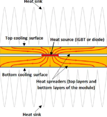
[image:5.612.315.562.314.474.2]from a thermal design perspective, as they are an integral part of the thermal management arrangement. The ceramic layers act as mechanical supports, electrical insulators and as good thermal bridges toward the cooling surfaces, because they have small thickness together with large area and good thermal conductivity. In other words, as illustrated in Fig. 13, from a thermal design point of view, the layers where IGBTs and diodes are soldered work as heat spreaders integrated in the module.
[image:6.612.341.534.221.537.2]Multi-domain physical simulation was used to carry out a detailed analysis and design refinement of a number of design features and parameters. This kind of analysis is essential for determining the maximum heat that can be generated in the IGBTs and the diodes for given assembly dimensions and given boundary conditions. So, it was also applied to the study of required heat-sinking solutions under representative operational conditions. To choose the heat sink it is necessary to evaluate the heat flux at the cooling surfaces. Both IGBTs and diodes are rated for a maximum operating junction temperature of 448 K.
Fig. 13. Schematic of the thermal management arrangement of the power switch module.
The main target of the thermal analysis is to assess the design requirements in order to keep a satisfactory margin from the maximum value at worst-case or maximum load/ambient temperature conditions. Here, we present the results of a steady-state analysis. The solution of the heat equation is based on the finite element method. As thermal load, a worst case was considered with a total dissipated power by the semiconductor devices of 300 W: 100 W generated inside each IGBT and 50 W generated inside each diode. These values correspond to a 10 kW inverter leg with a representative 97% efficiency. The low resistance of the copper traces allows neglecting of the Joule heating inside them. The thermal conductivities of the materials were set as follows [13-14]:
• kCu = 400 W/mK; • kSi = 130 W/mK; • kSi3N4 = 27 W/mK;
• kSn3.5Ag = 40 W/mK.
The heat-transfer coefficient for both the top and bottom cooling surfaces was initially set at a quite conservative value of h = 2400 W/m2K, to account for the whole thermal resistance between the cooling surface and ambient, including the contributions of a heat sink and a thermal conductive filler between the heat-sink and the cooling surface. The heat transfer coefficient of all the other surfaces was set to zero (adiabatic walls). In this case, ambient temperature was set at 293 K and a study was conducted using different heat generation profiles and different heat sink characteristics. Fig. 14 shows the resulting 3D thermal maps. The maximum temperature, reached inside the IGBTs, is around 387 K, well below the maximum limit of 448 K.
a)
b)
Fig. 14. Thermal maps (in K) obtained by a simulation of the power switch module with a total heat generation of 300 W, h=2400 W/m2K on cooling
surfaces and Tamb = 293 K: (a) external surfaces (top); (b) inner temperatures at
the silicon component layer.
III. COOLER
A. Cooler design
[image:6.612.85.263.302.497.2]dissipated power is 300 W, with a flow rate of 2 l/min and an inlet coolant temperature of 293 K.
High power inverters used, for instance, in transportation, need miniaturization and weight reduction (see [15], for example). This, in turn, requires cooling systems with high efficiency and reliability. Such inverters, either in research prototypes or commercially available power modules often introduce water or air cooled heat sink system [16, 17]. One of the goals of the cooling system design is to maintain the junction temperature of the power device below its maximum allowable temperature for nominal operation.
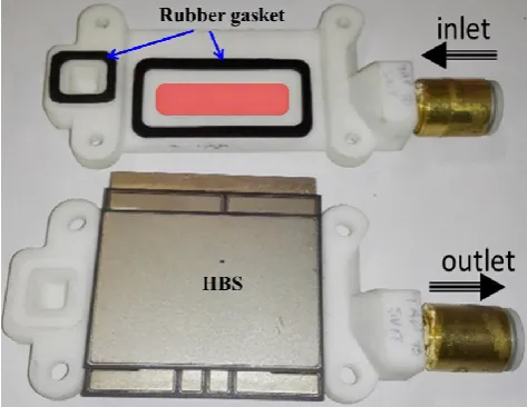
[image:7.612.339.533.48.575.2]The first version of the water cooling system developed here is shown in Fig. 15: it was designed so as to maximize cooling at the locations of the hot-spots (i.e., the in correspondence of the power devices), corresponding to the rectangular red-colored area in the top-side photograph of Fig.15. It is also considered that the restrictions which are imposed by the position of the inlet and outlet of the coolant including the bolting locations for the gasket and 3D print polyamide plastic cover are dependent on the packaging conditions. The liquid flows from the inlet toward the top cooling surface, and once it passes this surface, it turns down and flows via the bottom cooling area of the switch to get to the outlet. Rectangular gaskets were designed to seal the plastic and the switch cooling surface. Finally, the cooling system is assembled and fixed with screws. Its nominal performance was investigated and optimized with the help of fluid-dynamic computer aided simulation and yielded the nominal full load steady-state results shown in Fig. 16, which corresponded to the intended target for the devices used here (rated for up to 175 ºC steady junction temperature operation): as can be noted in Fig. 16 b) and c), the maximum temperatures of IGBTs and diodes were 323 K, 322 K, 333 K, 332 K for QH, QL, DH, DL, respectively.
Fig. 15 Liquid cooler prototype.
a)
[image:7.612.60.297.467.650.2]b)
Fig. 16. Cooler external (a) and internal temperature distribution (b); detail of estimated temperature on the semiconductor chips (c)
B. Experimental characterization
from this value the estimated power losses in the filter elements and their value indirectly verified by comparison of thermal measurements with structural thermal simulations, as discussed ahead.
TABLEI
THERMAL MEASUREMENTS OPERATING CONDITIONS
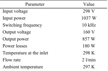
Parameter Value Input voltage 298 V Input power 1037 W Switching frequency 10 kHz Output voltage 160 V Output power 857 W Power losses 180 W Temperature at the inlet 298 K Flow rate 2 l/min Ambient temperature 297 K
[image:8.612.83.265.130.250.2]The cooling liquid inlet temperature was regulated by a liquid cooling system (Thermo Fisher Artic A25-SC100 refrigerated/ heated bath circulator) and a 40% propylene glycol was used for corrosion and frost protection. The top surface of the cooler was painted with high emissivity coating. Fig. 17 shows the external thermal map measured by the IR camera, which is in very good agreement with the values estimated using structural simulations (finite element method).
Fig. 17. Measured (left) and simulated (right) thermal map on the upper surface of the cooler + HBS assembly at the steady–state operating conditions of Tab. I.
IV. SYSTEM LEVEL INTERCONNECTION
In building a whole inverter, it is important that the electro-thermal and electro-magnetic advantages brought along by the integrated switch are not penalized at the moment of interconnecting more switches among them and with filters, gate drivers and the load. As part of this philosophy, in this work we also looked at integrating high-frequency decoupling capacitors as close as possible to the semiconductor devices.
For power ratings of few kW’s typical values for high frequency decoupling capacitors are in the range of few micro-farads. To contain parasitic inductance and resistance value it is moreover customary to implement these filters with either ceramic or film capacitor technology. The latter technology is however too bulky to be considered for an integration exercise, unless one can directly collaborate with capacitor
manufacturers or has in-house production capability. Ceramic technology offers much better capacity-density figures, but typically suffers from serious limitations in terms of capacitance value stability over bias voltage and temperature, with the result that, for application at few 100 V’s, as in this work, over design is typically required, consisting in the parallel connection of a relatively large number of components.
Moreover, the maximum operational temperature values are typically lower than what is realistically required for mounting in the close vicinity of power switches. More recently, a new family of capacitors has been introduced, so called CeraLinkTM capacitors, which is specifically designed for fast switching 650V semiconductors and offers new benchmark performance in terms of ratings, size and stability [18]. Fig. 18 shows a snapshot and indication of dimensions for a 1 μF-500 V nominal rating component; data-sheet information about capacitance stability over bias voltage and temperature indicate excellent stability [18]. In view of these characteristics, this is presently regarded by the authors as the best commercially available product for integration purposes.
[image:8.612.48.289.379.489.2]a) b)
Fig. 18. High frequency CeraLink capacitor: snapshot, a), and dimensions, b), of a 1μF-500 V component [18].
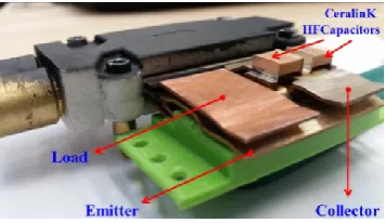
In moving to system level integration, it is very important to be able to place the high-frequency decoupling capacitors as close as possible to the switching devices. Ideally, these should be embedded within the HBS itself. However, in view of their relative thickness, it was preferred in this case to still keep them outside of the sandwich structure, since they would have impaired the ability to achieve an equally compact and high performing design. So, external power line connections were designed following the same philosophy applied to the switch to still contain overall parasitic inductance. A plug-in type flat connector was designed, inspired by the edge connectors used in high frequency signal and thus re-branded as power edge connector. The concept is illustrated in Fig. 19: the ceramic capacitors are embedded within the connector; inside the connector, folded metal clips ensure good mechanical and electrical contacts with the emitter, collector and load tabs of the switch. Fig. 20 shows a picture of the actually manufactured prototype, connected to the power switch (the cooler was painted black for experimental infrared thermal characterization). On the side not receiving the HBS power terminals, the connector is designed to receive a standard PCB, on which the DC-link capacitors are mounted.
connector is designed to receive on one side the HBS and on the other the logic circuitry in the gate-driver. Analog switches, capacitors and resistors belonging to the gate-driver circuit are housed within the connector itself, in the close vicinity of the HBS terminals.
[image:9.612.316.564.94.216.2]Fig.19. Power edge connector model with embedded high-frequency de-coupling capacitors.
Fig.20. Power edge connector prototype with detail of interconnection to the HBS.
a)
[image:9.612.104.243.116.244.2]b)
Fig. 21. Gate-side power edge connector: 3D CAD model a); and prototype b).
The resulting overall system level assembly, corresponding to the schematic functional inverter breakdown diagram of Fig.1, is shown in Fig. 22.
Fig.22. Photograph of the fully assembled inverter, corresponding to the schematic breakdown of Fig. 1.
The assembled single-phase inverter contains all components required for operation. All functional modules within the inverter system are interconnected by plug-in type connectors: so, failure of any one individual module requires dedicated maintenance, to replace the failed module only. With the proposed approach, that can be achieved quite speedily, as it does not require de-soldering or un-screwing of the modules, nor the replacement of interface materials, for instance, towards a heat-sink or mounting substrate. Connection to the loads and to the input power supply is implemented by means of the DC-link and load connections PCB-type board, which only mounts the DC-link electrolytic filter capacitors and foresees the use of cables and screwed terminals. It is important to note, that these terminals may not strictly need to be removed for repairing and maintenance purposes.
V. PRELIMINARY FUNCTIONAL TESTS
A preliminary full system functional test was carried out in open loop configuration, Fig. 23, with 300 VDC input voltage and 10 kHz switching frequency, with a fixed dead time of 500ns. The cooling liquid temperature was regulated to 25 ºC, using propylene glycol as the coolant. A dedicated test set-up was built, which accommodates additional filter elements (magnetics) and the driving platform, based on an Altera FPGA. Some representative waveforms are reported in Fig. 24. These results confirm the correct operation of the inverter and, albeit with relatively slow switching transitions, support the indication of contained value of parasitic inductance involved in the commutation process.
[image:9.612.85.263.280.383.2] [image:9.612.94.254.419.717.2] [image:9.612.312.566.633.719.2]a)
b)
Fig.24 Representative experimental result a); and zoomed version of voltage across the switch b).
VI. CONCLUSIONS
This paper has proposed an innovative modular integration scheme for power converters which brings along advanced electro-thermal and electro-magnetic performance, as well as modularity and reduced impact of single component failure for system maintenance and availability. The devised solution bases on a competitive assembly process, which can be made to reduce manufacturing time to compensate for somewhat higher material costs, as compared with traditional assembly processes. The benefits achieved at power switch level are kept when integrating a whole system by bespoke development of
power edge connectors with embedding capability for passive components and auxiliary circuitry. The proposed solution enables the development of modular power converters, thus potentially enabling significant gains in system level maintenance cost, which, again, are likely to offset any extra cost incurred due to initial higher price. Preliminary experimental results show correct operation of the system. More quantitative details of electro-thermal performance are presented in [19, 20]. Overall, the proposed approach is transferable to upcoming wide-band-gap device technology, as it is compatible with higher heat-generation rates and higher switching frequencies than the more traditional assembly solutions. Some specific features need of course re-design for the needs of the devices at hand. In the future, integration of magnetic components, neglected in this study, also needs to be looked at.
REFERENCES
[1] M. Mermet-Guyennet, New structure of power integrated module, in Proc. of the 4th International Conference on Integrated Power Systems (CIPS 2006), Naples, Italy, Jun. 7-9, 2006.
[2] P. Solomala, A. Castellazzi, M. Mermet-Guyennet, M. Johnson, New Technology and Tool for Enhanced Packaging of Semiconductor
Power Devices, in Proc. IEEE International Symposium on Industrial
Electronics (ISlE 2009), Seoul Olympic Parktel, Seoul, Korea July 5-8, 2009.
[3] C. M. Johnson et al., Compact Double-Side
Liquid-Impingement-Cooled Integrated Power Electronic Module, in Proc. of the 19th
International Symposium on Power Semiconductor Devices & ICs, May 27-30, 2007 Jeju, Korea.
[4] Z. Liang, J.D. van Wyk, F.C. Lee, Embedded Power: A 3-D MCM
Integration Technology for IPEM Packaging Application, IEEE
Transactions on Advanced Packaging, VOL. 29, NO. 3, August 2006. [5] J. Yin, Z. Liang, J.D. van Wyk, High Temperature Embedded SiC Chip
Module (ECM) for Power Electronics Applications, IEEE
Transactions on power electronics, Vol. 22, NO. 2, March 2007. [6] F.Z. Peng, Revisit Power Conversion Circuit Topologies–Recent
Advances and Applications, in Proc. of the 6th IEEE International
Power Electronics and Motion Control Conference (IPEMC/ECCE-Asia 2009), Wuhan, China, May 2009.
[7] A. K. Solomon., A. Castellazzi,, N. Delmonte, P. Cova, Modular Power Converter Integration based on Non-Conventional Power Switch
Assembly and Interconnects, 9th International Conference on Power
Electronics-ECCE Asia June 1 - 5, 2015, Seoul, Korea.
[8] A.Solomon, A. Castellazzi, Application driven integrated design of a
half-bridge power switch, ISPSD2011, San Diego,USA.
[9] A. K. Solomon, J. Li, A. Castellazzi, M. Johnson, Integrated
Half-Bridge Switch Using 70um Thin Devices and Hollow Interconnects,
IEEE Transactions on Industry Applications Vol. 51, Issue 1, 556 – 566, Jan.-Feb. 2015.
[10]J.L. Marchesini, Y. Avenas, P.O. Jeannin, S. Boulahrouz, Reduction of the stray inductance in a switching cell using the Power
Chip-On-Chip 3D integration concept,” 2012 IEEE Energy Conversion
Congress and Exposition (ECCE).
[11] A. E. Ruehli et al., Nonorthogonal PEEC Formulation for Time- and Frequency-Domain EM and Circuit Modeling, IEEE Transactions on Electromagnetic Compatibility, Vol. 45, No. 2, May 2003.
[12] http://www.cedrat.com/software/inca3d/
[13] T.Siewert, S. Liu, D. R. Smith, J. C. Madeni, “Database for Solder Properties with Emphasis on New Lead-free Solders, Properties of
Lead-Free Solders, Release 4.0”, National Institute of Standards and
Technology & Colorado School of Mines, 2002.
[14] Multiple authors, “Handbook of Lead-Free Solder Technology for
Microelectronic Assemblies”, CRC Press, 2004.
[9] G. Engelmann, M. Kowal, R.W. De Doncker, A highly integrated drive inverter using DirectFETs and ceramic dc-link
capacitors for open-end winding machines in electric vehicles”, 2015
IEEE Applied Power Electronics Conference and Exposition (APEC) [16]Burress, T. A. et aI, "Evaluation of the 2008 Lexus LS 600h Hybrid
Synergy Drive System," ORNLlTM- 20081185, UT-Battelle, Oak
Ridge National Laboratory, Oak Ridge, Tennessee, USA, Jan. 2009. [17]Y. Zhang, I. Belov, N.G. Sarius, M. Bakowski, H.P. Nee, P. Leisner,
Thermal evaluation of a liquid/air
cooled integrated power inverter for hybrid vehicle applications, 14th
International Conference on Thermal, Mechanical and Multi-Physics Simulation and Experiments in Microelectronics and Microsystems (EuroSimE), 2013.
[18]http://en.tdk.eu/tdk-en/1054426/products/productcatalog/ ceramic-capacitors/ceralink-capacitors--epcos-
[19] A. K. Solomon, A. Castellazzi, N. Delmonte, P. Cova, Modular
plug-in high-performance assembly of a power converter, in Proc.
EPE-ECCE Europe, 2016.
[20] P. Cova, N. Delmonte, A. K. Solomon, A. Castellazzi, Thermal design optimization of novel modular power converter assembly enabling
higher performance, reliability and availability, Microelectronics