Abstract— The thermomechanical reliability of SiC power devices and modules is increasingly becoming of interest especially for high power applications where
power cycling performance is critical. Press-pack
assemblies are a trusted and reliable packaging solution that has traditionally been used for high power thyristor-based applications in FACTS/HVDC, although press-pack IGBTs have become commercially available more recently. These press-pack IGBTs require anti-parallel PiN diodes for enabling reverse conduction capability. In these high power applications, paralleling chips for high current
conduction capability is a requirement, hence,
electrothermal stability during current sharing is critical. SiC Schottky diodes not only exhibit the advantages of wide bandgap technology compared to silicon PiN diodes, but they have significantly lower zero temperature coefficient (ZTC) meaning they are more electrothermally stable. The lower ZTC is due to the unipolar nature of SiC Schottky diodes as opposed to the bipolar nature of PiN diodes. This paper investigates the implementation and
reliability of SiC Schottky diodes in press-pack
assemblies. The impact of pressure loss on the electrothermal stability of parallel devices is investigated.
Index Terms— Semiconductor device packaging, Schottky diodes, Silicon carbide, pressure packaging
I. INTRODUCTION
ILICON carbide (SiC) is a wide bandgap semiconductor with electrical properties that make it a suitable semiconductor for high and medium voltage applications like industrial drives, HVDC and FACTS. However, in high power
This work was supported by the UK Engineering and Physical Science Research Council (EPSRC) through the Underpinning Power Electronics Devices Theme (EP/L007010/1), Components Theme (EP/K034804/1) and HUB (EP/K035304/1).
Jose Ortiz Gonzalez, Olayiwola Alatise, Li Ran and Philip Mawby are with the School of Engineering, University of Warwick, CV4 7AL, Coventry, United Kingdom. (e-mail:[email protected], [email protected], [email protected],
Attahir Murtala Aliyu and Alberto Castellazzi are with the Power Electronics, Machines and Control Group, University of Nottingham, Nottingham, UK, (e-mail: [email protected], [email protected])
Pusparajah Rajaguru and Chris Bailey are with the Computational Mechanics and Reliability Group, University of Greenwich, London,
United Kingdom. (e-mail: [email protected],
grid connected converters, silicon technology still dominates with 4.5 to 6.5 kV IGBT modules and 8 kV thyristor press-pack modules commercially available in high volumes. Be that as it may, as research advances are made in the epitaxial growth of wide area and thick SiC substrates with low defect densities, the power rating of SiC power devices is set to increase in the near future. Furthermore, as the issue of low minority carrier lifetimes in SiC is improved to enable conductivity modulation in bipolar devices, SiC IGBTs and GTOs with significantly higher voltage ratings will become a reality. 15 kV SiC IGBTs have been already been demonstrated alongside 15 kV SiC power MOSFETs [1].
A critical consideration of SiC that must be fully addressed before its widespread adoption in high power applications is its thermomechanical reliability under power cycling. It is well understood that the Coefficient of Thermal Expansion (CTE) mismatch between the semiconductor, the solder and the substrate causes stresses at the joints and material interfaces [2]. These repeated stresses accumulate damage at the critical interfaces at a rate that depends on the mission profile of the power module. As a result of plastic strain in the solder, solder voiding and die attach delamination occurs thereby increasing the junction-to-case thermal resistance of the power device. This increases the average junction temperature and the conduction and switching losses. Furthermore, as the voiding expands, the reliability of the module reduces since other temperature related failure mechanisms have a higher likelihood of activation. Another widely understood failure mechanism is gate/source wire-bond lift-off, again resulting from thermomechanical stresses under thermal cycling [2]. These phenomena are well understood for silicon technology however, the literature for SiC technology is sparser. There have been some investigations in [3] and [4] that showed reduced power cycling performance of SiC power devices compared to silicon power devices. The 3 times higher Young’s Modulus of SiC compared to silicon and the smaller die size were cited as the possible reasons behind the reduced power cycling capability of SiC modules.
The critical nature of grid connected converters and the high cost of failure due to the aforementioned failure mechanisms pushed design engineers into press-pack assemblies where the wire-bonds and die attach weaknesses are obviated [5]. Several decades of experience and field data with press-pack assemblies has given power electronic
Evaluation of SiC Schottky Diodes Using
Pressure Contacts
Jose Ortiz Gonzalez,
Student Member, IEEE
, Olayiwola Alatise, Attahir Murtala Aliyu,
Pushparajah Rajaguru, Alberto Castellazzi, Li Ran,
Senior Member, IEEE
, Philip Mawby
Senior Member, IEEE
and Chris Bailey
engineers increased confidence in the technology. Here, the semiconductor is pressed between two copper electrodes using an intermediate material to match the CTE of both materials. The main benefits of press-pack modules [5] are a compact design, possibility of double side cooling, higher reliability due to the elimination of the solder and wirebonds and a reduced number of interconnections of materials with different CTE. On the other hand, the lack of dielectric insulation and a more complex mechanical assembly are the major tradeoffs. Press-packs were historically adopted for wafer-based devices like thyristors, however, more recently IXYS [6] and ABB [7] have commercialized press-pack assemblies for chip based devices like IGBTs, which have been evaluated and studied in [8-10]. One of the most interesting properties of these modules is the ability to fail into a stable short-circuit [11] which is a feature of interest for topologies that require series-connected devices.
The technological migration from line commutated converters to voltage source converters has made press-pack IGBTs an attractive technological proposition and 3L-NPC converters for large wind turbines on the grid-side have already been evaluated [12-13]. These press-pack IGBTs are co-packaged with PiN diodes to enable reverse current conduction capability, several of which are connected in parallel for high current conduction capability. The possibility of co-packaging these press-pack IGBTs with SiC Schottky diodes is interesting, given that Schottky diodes exhibit better electrothermal characteristics compared to PiN diodes. SiC Schottky diodes, unlike PiN diodes, have no reverse recovery characteristics because they are unipolar and their lower Zero Temperature Coefficient (ZTC) point makes them more electrothermally stable when sharing currents in parallel. Hence, this paper investigates the performance of SiC Schottky diodes in press-pack both in terms of reliability and electrothermal stability under parallel conditions. Section II addresses the electrothermal and reliability performance of SiC Schottky diodes in traditional discrete packages by using measurements and finite element models to analyze the stresses in the solder. Section III presents a prototype for the evaluation of a SiC Schottky diode using pressure contacts, showing the characterization of the electrothermal properties for different clamping forces. Section IV presents the power cycling performance of the SiC press-pack assembly. Section V investigates the impact of pressure imbalance in parallel connected devices while section VI concludes the paper.
II. EVALUATION OF SILICON CARBIDE DEVICES IN TRADITIONAL PACKAGING SYSTEMS
A. Electrothermal stability of paralleled diodes
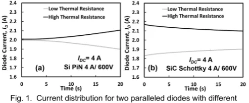
Fig. 1 shows the ON-state current conducted by 2 parallel diodes with Fig. 1(a) showing parallel PiN diodes and Fig. 1(b) showing parallel Schottky diodes. The PiN diodes are 600 V devices with datasheet reference HFA04TB60, while the
Schottky diodes are 600 V devices with datasheet reference C3D02060A and C3D02060F. Current sharing between the 2 diodes during ON-state was evaluated for both diode technologies by passing a DC current of 4 A through the parallel pair and introducing a variation in the thermal resistance between the parallel pair to investigate how current imbalance occurs. The variation in the thermal resistance between the parallel pair is meant to emulate degradation like solder voiding in a traditional package or loss of force contact in a pressure-contact package. It can be seen by comparing the 2 technologies in Fig. 1 that the current in the SiC Schottky diode converges while the current in the silicon PiN diode diverges. This is because of the lower ZTC in SiC Schottky diodes compared to silicon PiN diodes. Hence, current is positively correlated with temperature in the PiN diode pair while current is negatively correlated with temperature in the SiC Schottky diode pair.
B. Power cycling of SiC in TO-247 packages
Thermal cycling testing is a useful tool to understand the performance of a packaging system under temperature cycling. When the temperature variations are generated by the self-heating of the device it is called power cycling [14] and in some cases it requires the ability to identify the junction temperature (TJ), as monitoring the thermal resistance is a
good cursor of degradation, with an increase of 20 % of the junction-to-case thermal resistance (RTH,J-C) considered a
failure [5]. Characterizing the thermal transient impedance is an effective way of monitoring the health of the packaging system, as it allows the identification of the degraded element of the packaging. The structure function is a special function obtained from the transient cooling or heating curves using direct mathematical transformations [15-16].
This mathematical approach uses thermal resistances and capacitances in the Cauer form to identify changes in the thermal structure of the module. Two types of structure functions are defined: differential and cumulative structure functions. The differential structure function, given by (1), is defined in [17] as the derivative of the cumulative thermal capacitance with respect to the cumulative thermal resistance, where a peak represents a new interface in the heat flow path.
[image:2.595.303.550.85.187.2]( ) = (1)
The cumulative structure function is the representation of the sum of the thermal capacitances as a function of the sum of the thermal resistances. When this structure function is discretized, it results in a Cauer network, which has a link to the real structure of the device, where a change in the slope represents a change of material. Dedicated thermal impedance characterization equipment [18], which can also perform power cycling, was used for obtaining the differential and cumulative structure functions of a SiC device model C3D25170H from CREE/Wolfspeed in a TO-247 package and they are presented in Fig. 2 and Fig. 3 respectively.
The changes in thermal resistance of the package, caused by the degradation of the packaging during power cycling can be identified in the structure functions. Solder voids and cracks in the solder caused by the higher stresses on the die attach layer, increase the value of the thermal resistance, shifting the structure function to the right [19].
Using the thermal characterization equipment [18], the SiC device was subjected to power cycling using a heating current of 30 A for 30 s with a cooling time of 30 s. In this accelerated degradation tests, the number of cycles to failure is inversely proportional to the junction temperature excursion (∆TJ) and
for this particular test, the resulting∆TJ was 53.1 °C, with a
maximum temperature of 96.6 °C.
The total number of cycles recorded was 19000, with the
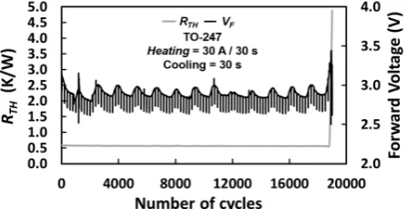
transient thermal impedance characterized every 200 cycles. The measured thermal resistance (RTH) and forward voltage
(VF) across the diode during the power cycling tests are shown
in Fig. 4.
From the results presented in Fig. 4, it can be seen that there was no observable thermal impedance degradation during the power cycling test. However, the result of the power cycling experiment is catastrophic failure after 19000 cycles. The forward voltage was characterized during the cycling process and an 18% increase in the forward voltage was observed at the point of failure. The spikes shown on the forward voltage in Fig. 4 are due to the thermal impedance characterization which occurs every 200 cycles. The low frequency oscillation is due to temperature variation between night and day.
C. Finite Element Analysis of the stresses in the solder Finite Element Analysis (FEA) has been used to evaluate the results presented in the previous section. The test vehicle shown in Fig. 5 was used to evaluate the impact of the chip material on the stresses on the solder. The dimensions of the substrate selected are 20.4 mm by 20.4 mm and both pure copper and Direct Bonded Copper (DBC) substrates were evaluated. The thickness of the copper substrate is 1.5 mm, while the thicknesses of layers of the DBC substrate made of Copper-Aluminum Oxide- Copper are 0.3 mm, 1 mm and 0.1 mm respectively [5]. The solder selected is Sn3.5Ag with a
thickness of 100 μm and a wetting angle of 33°. A SiC
Schottky diode model CPW5-1200-Z050B from
CREE/Wolfspeed and a Si PiN diode model 5SLY 12E1200 from ABB, both 1200 V/ 50 A devices, were selected as the devices for these FEA studies. The dimensions of the chips, extracted from the datasheets, are 4.9 mm by 4.9 mm with a
thickness of 380 μm for the SiC chip and 6.3 mm by 6.3 mm with a thickness of 350 μm for the Si device.
The tridimensional finite element model shown in Fig. 5
was generated in ANSYS FEA [20] and passive
[image:3.595.70.255.87.302.2]thermomechanical analysis was performed using the package SOLID185, with the material properties defined in [3][21], Fig. 2. C3D25170H Differential structure function
[image:3.595.55.279.618.733.2]Fig. 4. Evolution of forward voltage and thermal resistance during power cycling of the C3D25170H
Fig. 5. Test vehicle used for analyzing the stresses on the solder. (a) SiC die (b) Si die
Fig. 3. C3D25170H Cumulative structure function
TABLE I
MATERIAL PROPERTIES OF THE SEMICONDUCTORS EVALUATED IN THE FEA SIMULATIONS
Material property Si SiC
Density (kg/m3) 2300 3210
Thermal Capacity (J/kg°C) 700 690
Thermal Conductivity (W/m°C) 160 380
CTE (μm/m°C) 3 4.3
where the metallization of the chips was ignored for the calculations. The properties of the Sn3.5Ag solder where extracted from [22], using the Anand viscoplastic model from [23]. The main material properties of the semiconductors are shown in Table I, where it can be observed that the principal differences between SiC and Si are the thermal conductivity and the Young’s modulus, along with a die size which is 65% larger for the Si device, as can be observed in Fig. 5.
The structural boundary condition in the FEA modelling is the three point freedom restraining boundary. The three degrees of freedom are fixed for one of the lower corners of the substrate, two degrees of freedom are fixed for a second lower corner with one degree of freedom fixed for a third lower corner. Considering the reduced complexity of the model, the FEA was performed for the whole geometry, instead of the quarter region approach, given the symmetrical properties of the model.
The passive thermal stress cycle used in this FEA study was -25°C/50°C, with a ramp time of 3 minutes and a dwell time of 15 minutes. The simulation results show that the higher stresses are on the solder/chip interface and 3D plots of the solder showing the interface are presented in Fig. 6 and Fig. 7. Fig. 6(a) shows the stresses in the solder layer for a SiC die on a DBC substrate, while Fig. 6(b) shows the same 3D plot for a pure copper substrate. Fig. 7 shows FEA simulation results for Si and SiC dies on copper substrates. It can be observed from Fig. 7, that, for the same substrate, the stresses are higher when a SiC chip is used compared to a silicon one. These higher stresses on the corners of the solder/chip interface generate cracks in the solder, leading to a higher thermal resistance or even catastrophic failures, as was shown in section II.b.
In the case of lead free solder with creep properties, the accumulated plastic strain on the solder can be used to estimate the lifetime using a Coffin-Manson model [24] using (2), where ∆εin is the accumulated equivalent inelastic strain
during a cycle, Nf is fatigue life, k is the fatigue ductility
exponent andCis the fatigue ductility coefficient.
∆ = (2)
Simulating the complete number of cycles to failure is computationally expensive, hence the stabilized accumulated plastic strain value at the fourth cycle was used. The accumulated plastic strain in one cycle is calculated using volume averaging area for a layer of solder with a thickness of
10 μm close to the chip, while the values used for the
[image:4.595.313.541.275.318.2] [image:4.595.314.539.448.491.2]Coffin-Mason model have been extracted from [24], withk= 0.6978 andC= 3.921. Table II presents the accumulated plastic strain values for the different die/substrate combinations evaluated.
TABLE II
ACCUMULATED PLASTIC STRAIN FOR ONE CYCLE -25 °C/+50 °C
Si SiC
Copper Substrate 0.00835 0.01214
DBC Substrate 0.00445 0.00468
The cycles to failure calculated from the accumulated plastic strain are presented in Table III, where it can be observed that the lifetime of the solder when SiC is used is lower compared with the lifetime for Si chips, especially for the copper substrate. From the FEA results, it can also be observed how improvements on the packaging, like using a substrate which matches the CTE of the semiconductor, can lead to an enhanced power cycling capability.
TABLE III
CYCLES TO FAILURE FOR A THERMAL CYCLE OF -25 °C/+50 °C
Si SiC
Copper Substrate 6771 3945
DBC Substrate 16332 15461
III. PROTOTYPE FOR THE EVALUATION OF SILICON CARBIDE DEVICES USING PRESSURE CONTACTS A prototype for the evaluation of pressure contacts on SiC Schottky diodes has been designed and initially evaluated in [25]. Fig. 8 shows the prototype of a fully floating press-pack diode, including copper poles, intermediate contacts, the semiconductor chip and the housing. The prototype is for a single diode chip and it has been designed for a 1200V/50A SiC Schottky diode model number CPW5-1200-Z050B from CREE/Wolfspeed. The size of the chip is 4.9 mm by 4.9 mm, with an anode opening of 3.8 mm by 3.8 mm and a thickness of 380 μm. The intermediate contacts for matching the CTE are made of molybdenum, with a size of 3.7 mm by 3.7 mm for the anode contact and 4.9 mm by 4.9 mm for the cathode contact. These contacts have a thickness of 1.5 mm and have been machined with a radius of 0.5 mm. The pressed area is 13.48 mm2 for the anode contact and 23.80 mm2 for the
cathode contact. A die carrier made of PPS is used for the alignment of the chip and the intermediate contacts while an external case made of PEEK is used for positioning the anode and cathode poles, made of copper with a 5μm nickel plating. Both PPS and PEEK are engineering plastics with a Fig. 6. Von Mises stress on the solder layer for a SiC die. (a) DBC
substrate (b) Copper substrate
[image:4.595.48.291.514.603.2] [image:4.595.70.256.633.728.2]temperature of operation over 220 °C, dimensionally stable, easy to machine and UL94/V0 compliant [26]. Fig. 9(a) shows the die carrier and the anode contact, while Fig. 9(b) shows the picture of the prototype fully assembled
A pressure ranging from 10 N/mm2to 20 N/mm2is defined
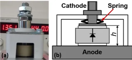
in [5] for optimal electrical and thermal contact hence, clamping forces ranging from 300 N to 500 N were selected for the studies presented in this paper. The clamping force is applied using box clamps model BX42 from GD Rectifiers [27]. The clamp BX42 is a commercially available clamp and the assembly of the clamp with the module is shown in Fig. 10(a). The clamp uses springs to apply the force on the module and is calibrated at a nominal clamping force for the height h (19.38 mm) of the prototype. During the assembly, the four bolts of the BX42 clamp are tightened sequentially, in order to achieve the best compensation possible and the design of the clamp ensures that the force applied by the spring is orthogonal to the surface of the module. The principle of operation of the clamping mechanism is shown in Fig. 10(b).
The cumulative structure function for clamping forces of 300 N and 500 N is presented in Fig. 11. In this figure, the impact of the clamping force on the thermal impedance is clearly identified. Increasing the clamping force shifts the cumulative structure function to the left, indicating a reduction on the thermal resistance.
The thermal resistances and capacitances are determined by the material properties, but when pressure contacts are used, a contact resistance is added to the static thermal network, as it is shown in Fig. 12 [28], where the contact resistances (Rth,material-material) and thermal resistances (Rth,(material)) are
identified for the different elements of the press-pack module. The contact resistance is a function of the clamping force and it is also affected by properties like the flatness, roughness, metallization of the elements in contact and hardness [29]. For a transient thermal impedance analysis the thermal capacitances are added to the thermal network.
Fig. 12 shows a double side cooled assembly, where both anode and cathode poles are connected to a heatsink, and the case temperature (TC) on both sides is assumed to be equal.
The junction temperature (TJ) is defined as the temperature at
the center of the die. The characterization of the press-pack module shown in Fig. 11 was done using a single side cooling system, where the anode pole, as can be seen in Fig. 8 and Fig. 10, was connected to the heatsink. Hence, the direction of heat flow in Fig. 12 is from the device (labelled D) through the intermediate contact (labelled C), through to the anode pole which comprises of a protruding section (labelled B) and the base (labelled A) which is connected to the heatsink. The thermal resistance is given by (3), wheredis the thickness of the material, A the cross-section and λTH the thermal
conductivity.
[image:5.595.319.530.81.189.2], = (3)
Fig. 8: Prototype of the SiC Schottky diode using pressure contacts
Fig. 9. (a) Detail of the assembly of the die carrier and the anode contact, (b) Fully assembled prototype
[image:5.595.57.286.85.184.2]Fig. 10. (a) Box clamp assembled, (b) Operation of the clamp
[image:5.595.58.286.205.306.2]Fig. 11. Impact of the clamping force on the cumulative structure function for the press-pack diode
[image:5.595.308.549.510.727.2] [image:5.595.56.282.632.735.2]The thermal resistance is inversely proportional to the cross-sectional area of the material and directly proportional to the length of the thermal path. The thermal path (from D to A) of the single side cooled prototype shown in Fig. 12, coupled with additional contact resistances, will yield a higher thermal resistance compared to traditional solder based systems. However, using a double side cooling system, which is one of the main benefits of the press-pack assembly, will minimize the impact of the pedestal on the thermal performance. Here, with respect to Fig. 12, the heat will flow from the device (D) to both poles (A and F). Hence, the single side cooled prototype presented here, has not been designed for an optimal thermal performance, nevertheless, it is suitable for the evaluation of the impact of the clamping force on the electrical and thermal characteristics as well as an assessment of its reliability.
Referring back to Fig. 11, the thermal resistance for a clamping force of 300 N force isRTH-300N= 2.31 K /W while
for a clamping force of 500 N, the measured value isRTH-500N
= 2.16 K/W, indicating a global reduction of thermal resistance of 0.15 K/W. Increasing the clamping force has also an impact on the electrical contact resistance and this has been evaluated. The impact of the electrical contact resistance on the forward voltage has been evaluated using the experimental set-up represented by the schematic diagram shown in Fig. 13, where the box clamp was attached to a heatsink model PS136/150B from GD Rectifiers [27]. In this set-up, the heating current is passed through the diode to raise the junction temperature through the self-heating of the device. A low sensing current is used to measure the junction temperature through the forward voltage and an auxiliary diode is used for isolating both power supplies.
The different thermal resistances and forward voltages that result from the different clamping forces cause different junction temperatures on the chip. This can be measured using the forward voltage measured at low current as Temperature Sensitive Electrical Parameter (TSEP) [30].
This is done after the heating current is switched off and the sensing current is used to measure the forward voltage during the cooling phase of the device. However, the temperature dependency of the forward voltage must first be determined so that a look-up-table or a calibration table can be created and used to translate measured forward voltages into junction temperatures. This calibration table was developed by measuring the forward voltage at different temperatures after the junction temperature of the device was set by a thermal chamber. By allowing enough time to reach steady state, the temperature of the chamber can be considered equal to the junction temperature. Using a sensing current of 200 mA, the forward voltage was measured at different temperatures for
clamping forces of 300 N and 500 N. The calibration curve is shown in Fig. 14.
Different magnitudes of DC heating currents each 15 seconds long were used for evaluating the electrical and thermal characteristics of a single diode module with pressure contacts applied by 300 N and 500 N clamps. The results for the forward voltage are presented in Fig. 15 for both 300 N and 500 N forces. Heating currents ranging from 6 A to 30 A were used. From these measurements it can be observed that a reduced clamping force increases the forward voltage of the diode for the same current, hence leading to higher power losses in that chip. This is expected since the electrical contact resistance is inversely proportional to the clamping force and the forward voltage is proportional to the contact resistance.
The impact of the clamping force can be evaluated using the measured forward voltage across the prototype. Using the simplified schematic shown in Fig. 16, where the electrical contact resistances (Rmaterial-material) and electrical resistances
(R(material)) are identified for the different elements of the
press-pack module, the forward voltage across the module for a current I, VF,I, is given by (4). In (4), VAK,I is the forward
voltage across the chip for that currentIwhileΣRX(Material)and ΣRX-Y are the sum of the electrical and contact resistances
respectively.
, = , + ∙ ( )+ (4)
[image:6.595.340.513.87.225.2]The only term in (4) directly dependent of the clamping force is the contact resistance RX-Y. Hence, assuming
[image:6.595.330.516.574.728.2]Fig. 14. Calibration of the forward voltage as TSEP
Fig. 13. Schematic of the circuit for evaluation of the impact of the
temperature invariance for short current pulses, the internal diode forward voltage and the voltage drop across the contacts can be assumed constant. The measured voltage across the press-pack assembly, including the clamp and heatsink, for a series of currents ranging from 10 to 30 A, at 300 N and 500 N clamping forces, is presented in Table IV. The relationship between the contact resistances at two different forces can be written as (5) which was used for calculating the difference in contact resistance caused by the different clamping force. The forward voltage was measured after 20 ms, using the data from Fig. 15. The average contact resistance reduction from using a clamping force of 500 N instead of 300 N is 1.748
mΩ.
, − , = ∙ − (5)
TABLE IV
IMPACT OF THE CLAMPING FORCE ON THE FORWARD VOLTAGE AND CONTACT RESISTANCE
Current
(20 ms pulse)(A) V
300N,I
(V) V
500N,I
(V) ΣRX
-Y-ΣRX-Y
(mΩ)
10 1.0597 1.0423 1.741
14 1.1185 1.0944 1.723
18 1.1756 1.1445 1.702
22 1.2320 1.1953 1.669
26 1.2956 1.2470 1.867
30 1.3541 1.3005 1.786
The junction temperature increase for the different DC heating pulses is presented in Fig. 17, where the junction temperature rise is shown as a function of the DC heating current magnitude. It can be seen that the temperature rise reduces with the increased clamping force. Hence, it is important in pressure contact power modules that the clamping force remains as constant and homogeneous among the different chips as possible over the mission profile of the application. Loss of contact force will increase the thermal
resistance and junction temperature. In section IV, results of the pressure package under power cycling using the same methodology as was used for the discrete TO-247 package are presented.
IV. POWER CYCLING OF SILICON CARBIDE IN PRESS-PACK The usual failure mechanism during power cycling of a solder based package system is the degradation of the solder, which causes an increase of the thermal resistance. In [19], changes in the cumulative function are used to identify the solder degradation of the packaging. In the case of press-pack assemblies, the lack of solder suggests a better thermal cycling performance hence, in order to verify this, the press-pack assembly proposed in section III was subjected to the same thermal cycling test as the TO-247 device, which failed catastrophically, using a heating current of 30 A during 30 s, with a cooling time of 30 s. The test performed was based on using the same heating pulse for both packaging technologies and in the case of the press-pack assembly, the resulting junction temperature excursion was 78.1 °C, with a maximum temperature of 118.5 °C, higher than the TO-247 power cycling test.
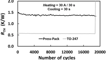
The transient thermal impedance was characterized every 200 cycles. The comparison of the degradation of the thermal resistances for both packaging techniques is presented in Fig. 18, where it is shown that the pressure contact assembly passes the number of cycles which triggered failure in the TO-247 package. This is despite the higher junction temperature excursion and the higher maximum junction temperature in the press-pack prototype. The plot of the thermal resistances as a function of the number of cycles presented in Fig. 18 shows no overall increase in the thermal resistance during the power cycling of the press-pack, although there is periodic variation in the values. This is due to periodic variation in the pressure at the interfaces during the power cycling, which is inevitable because of continuous expansion/contraction of the die and intermediate contacts. The higher value of the thermal resistance of the press-pack diode compared with the solder based TO-247 has been explained in section III. The approach of sintering the semiconductor to one of the intermediate contacts has already been proposed [5][31], however, given the reliability limitations of the solder layer for SiC devices shown in section II, the reliability of this proposed technique should be fully understood and characterized.
[image:7.595.80.262.89.176.2] [image:7.595.315.528.616.737.2]In the case of multichip chip modules, reduced contact force on individual chips during power cycling was identified in Fig. 16. Electrical schematic of the press-pack diode
Fig. 17. Impact of the clamping force on the junction temperature
increase for different heating pulses Fig. 18. Thermal impedance degradation. SiC TO-247 and
[image:7.595.81.254.619.730.2][32] as a possible failure mechanism of press-pack IGBT modules. Pressure imbalance appears as an added variable to the problem of paralleling multiple chips. Moreover, as it was mentioned in section III, the press-pack assemblies require a more complex mechanical system that is used to apply an external force to achieve perpendicular and equally distributed force across the whole surface of the module. Temperature variations can also affect the clamping system leading to a non-equally distributed force, which would have considerable impact on multiple chip modules, hence, the impact of pressure imbalance in multichip SiC Schottky diode modules using pressure contacts is evaluated in section V.
V. MULTIPLE CHIP MODULES
If SiC devices are to be used in press-pack applications, then high current multi-chip assemblies are inevitable. Hence, a 200 A SiC Schottky diode press-pack module was designed and assembled. Fig. 19 shows a picture of the press-pack prototype together with its 3D model.
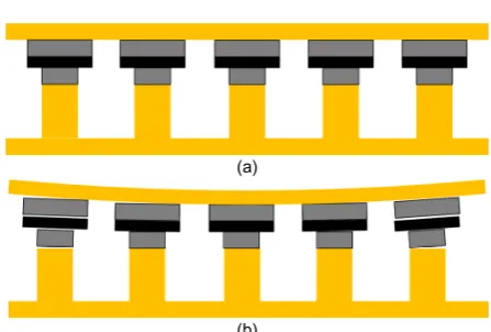
In multi-chip modules, maintaining equal pressures across all chips is critical for ensuring optimal current sharing between the parallel devices. In large area devices like thyristor wafers, unequal pressure over the area of the device will lead to hotspots on the wafer. In the case of multi-chip press-pack power modules, devices with lower contact force will exhibit higher junction to case thermal resistance and higher electrical resistance thereby diverting current to devices with higher contact force. Commercially available press-pack IGBTs have been designed using two techniques. In one design [6], the pressure is maintained by a global contact common to all devices as shown in Fig. 20(a). It can be seen
from Fig. 20(b) that reduced pressure and loss of contact is possible if there is mechanical deformation of the global contact. In the other design [7], individual springs are used to maintain the pressure on each IGBT/diode chip with the force on the chip determined by the product of the spring constant and the distance travelled by the spring. In both designs, unequal pressure will lead to current imbalance and reduced reliability. The proposed module, based on the approach presented in [6], will be clamped using an external force which will be ideally equally distributed, but, as it has been presented in section IV, this force changes during power cycling of the device and it will affect the current distribution.
In order to study how the pressure imbalance affects the current distribution and the forward voltage, the test configuration described in Fig. 13 was adapted for using 2 press-pack modules in parallel. This study was performed using a single chip module on each clamp and the modified electrical schematic is shown in Fig. 21 while the connection of the two diodes is shown in Fig. 22, where the heatsink PS136/150 is also shown. Diodes with similar forward voltages were selected for paralleling, but it is important to mention that there are multiple factors that will affect the forward voltage of the assembly, like the mechanical tolerances, flatness and roughness of the surfaces in contact, underlining the importance of the mechanical assembly for press-pack modules. The approach presented in [7], where an individual spring is used for each die would be less sensitive to dimensional tolerances and thermomechanical deformations.
Tektronix current probes model TCP303 were connected to each press-pack module to measure the current through each diode. Two scenarios were evaluated in case of imbalance of the clamping force: case A where both clamps are completely tight and the clamping forces are the nominal values, namely
[image:8.595.60.265.456.549.2]FD1=500N and FD2=300 N, and case B, where the 4 bolts of
Fig. 19. Multichip press-pack SiC Schottky diode (a) Prototype (b) 3D model
(a)
(b)
[image:8.595.312.537.507.734.2]Fig. 20. Impact of thermal expansion on the press-pack module during operation. (a) No deformation (b) deformation
Fig. 21. Schematic of the test configuration for evaluation of the impact of the pressure imbalance
[image:8.595.51.275.580.731.2]the clamp ofD2were tightened by hand thereby resulting in a
clamping force lower than 300 N as the spring compression is less than its nominal value. The first case is a mild case of pressure imbalance whereas the second case is more severe. A sensing current of 200 mA was passed through the parallel press-pack devices and the individual currents were measured at ambient temperature (25 °C) using the Tektronix TCP303 current probes. The current distribution between each device is shown in table V where it can be seen that the device with the higher clamping force conducts more current as expected. The current disparity is proportional to the pressure disparity since the more severe case of pressure imbalance leads to a higher current imbalance.
TABLE V
IMPACT OF THE CLAMPING FORCE IMBALANCE ON THE SENSING CURRENT DISTRIBUTION
Clamping Forces ID1(mA) ID2(mA)
FD1= 500 N /
FD2=300 N 101.2 99.7
FD1= 500 N /
FD2= loose clamp 109.6 92.7
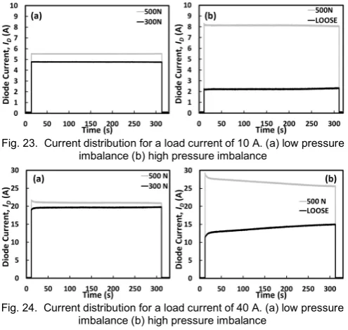
DC heating pulses of 10 A and 40 A, with a duration of 300 seconds were used to evaluate the impact of the pressure imbalance on current distribution between the parallel diodes. Fig. 23 shows the impact of the imbalance of the clamping
force for a load current of 10 A for the two scenarios described previously: (a) for a clamping force imbalance 300 N/ 500 N and (b) 500 N / loose clamp. Fig. 24 shows the impact of the pressure imbalance on the current distribution when the load current is 40 A. Fig. 25 presents the forward voltage of the paralleled diodes for both load currents and clamping imbalance scenarios.
In both cases, the pressure imbalance leads to a higher voltage across the paralleled diodes, increasing the power dissipated, as the results on Fig. 25 show. In the case of the results in presented in Fig. 23(a), where the load current is below the ZTC of the SiC Schottky diode evaluated it can be concluded that the low self-heating at that current levels has no noteworthy impact on the current distribution. If the pressure imbalance is high, from the results on Fig. 23(b) it can be observed that the ratio between both currents increases considerably. For a current level above the ZTC and a small pressure imbalance, the currents converge when the device carrying more current gets hotter, as the results on Fig. 24(a) show. For a high pressure imbalance, Fig. 24(b) presents a considerable difference in the shared current. The initial dip in the current is caused by the thermal response to the initial current imbalance. The currents converge due to the positive temperature coefficient of the Schottky diodes at that current level.
In silicon PiN diodes, the increase in minority carrier lifetime with temperature creates a higher carrier density in the drift region which causes the ZTC point to be higher compared to SiC Schottky diodes which are unipolar [33]. The higher ZTC cause the hotter device to conduct more current, as it was shown in Fig. 1(a) and the possibility of thermal runaway becomes more likely. In the case of a multi-chip SiC Schottky diode using pressure contacts, loss of pressure uniformity will cause current imbalance, however, the lower ZTC makes this imbalance electrothermally stable.
Current press-pack IGBT modules use Si PiN diodes to enable reverse conduction, however the better performance of SiC Schottky diodes under pressure imbalance when devices are paralleled, in addition to the superior switching properties of SiC devices, suggest that hybrid press-pack Si IGBT modules with SiC Schottky diodes can be a suitable packaging alternative.
The change in the current distribution between the chips in the module can be used for monitoring the pressure imbalance between chips. Current sensors distributed within the module, which would monitor the current through the chips can be used for inferring the pressure distribution. It can be done at low currents, as the results on Table V suggest or at higher currents during operation.
VI. CONCLUSION
A SiC Schottky diode in pressure contact assemblies was demonstrated and electrothermally characterized in this paper. The reliability under power cycling was shown to be better than TO-247. The clamping force was shown to be important in determining the thermal and electrical contact resistances and junction temperature. The lower ZTC in SiC Schottky Fig. 23. Current distribution for a load current of 10 A. (a) low pressure
[image:9.595.45.293.396.631.2]imbalance (b) high pressure imbalance
[image:9.595.41.289.636.733.2]Fig. 24. Current distribution for a load current of 40 A. (a) low pressure imbalance (b) high pressure imbalance
diodes compared to silicon PiN diodes meant that they were electrothermally stable under current imbalance resulting from the loss of pressure uniformity. Hence, as the voltage rating of SiC power devices increases in the near future, pressure contacts can be a suitable packaging solution for enhancing the reliability of the technology.
REFERENCES
[1] K. Vechalapu, S. Bhattacharya, E. Van Brunt, S. H. Ryu, D. Grider and J. W. Palmour, “Comparative evaluation of 15 kV SiC MOSFET and 15 kV SiC IGBT for medium voltage converter under same dv/dt conditions” IEEE ECCE 2015 Conference, September 2015
[2] M. Ciappa, “Selected failure mechanisms of modern power modules,” Microelectronics Reliability, vol. 42, no. 4–5, pp. 653–667, April–May 2002
[3] C. Herold, M. Schaefer, F. Sauerland, T. Poller, J. Lutz and O. Schilling “Power cycling capability of Modules with SiC-Diodes,” CIPS 2014 Conference, Nuremberg, Germany, 2014, pp. 1-6.
[4] L. A. Navarro, X. Perpina, P. Godignon, J. Montserrat, V. Banu, M. Vellvehi and X. Jorda “Thermomechanical assessment of die-attach materials for wide bandgap semiconductor devices and harsh environment applications,” inIEEE Transactions on Power Electronics, vol. 29, no. 5, pp. 2261-2271, May 2014
[5] J. Lutz, H. Schlangenotto, U. Scheuermann and R. De Doncker,
Semiconductor power devices: Physics, characteristics, and reliability. Springer Verlag, 2011.
[6] IXYS Press-Pack IGBT modules [Online]. Available: http://www.westcode.com/ppigbt.html
[7] ABB StakPak modules [Online]. Available: http://new.abb.com/semiconductors/stakpak
[8] F. Wakeman, K. Billett, R. Irons and M. Evans, "Electromechanical characteristics of a bondless pressure contact IGBT," Applied Power Electronics Conference and Exposition, 1999. APEC '99. Fourteenth Annual, Dallas, TX, 1999, pp. 312-317 vol.1.
[9] T. Poller, T. Basler, M. Hernes, S. D’Arco, J. Lutz, Mechanical analysis of press-pack IGBTs, Microelectronics Reliability, Volume 52, Issues 9– 10, September–October 2012, Pages 2397-2402
[10] S. Eicher, M. Rahimo, E. Tsyplakov, D. Schneider, A. Kopta, U. Schlapbach and E. Carroll., "4.5kV press pack IGBT designed for ruggedness and reliability," Conference Record of the 2004 IEEE Industry Applications Conference, 2004. 39th IAS Annual Meeting., 2004, pp. 1534-1539 vol.3.
[11] S. Gunturi and D. Schneider, "On the operation of a press pack IGBT module under short circuit conditions," in IEEE Transactions on Advanced Packaging, vol. 29, no. 3, pp. 433-440, Aug. 2006.
[12] O. S. Senturk, S. Munk-Nielsen, R. Teodorescu, L. Helle and P. Rodriguez, "Power density investigations for the large wind turbines' grid-side press-pack IGBT 3L-NPC-VSCs," 2012 IEEE Energy Conversion Congress and Exposition (ECCE), Raleigh, NC, 2012, pp. 731-738.
[13] K. Ma, "Chapter 2 - Promising Topologies and Power Devices for Wind Power Converter," in Power Electronics for the Next Generation Wind Turbine System, Springer International Publishing, 2015, pp. 19-29. [14] L. R. GopiReddy; L. M. Tolbert and B. Ozpineci “Power cycle testing of
power switches: A literature survey,” in IEEE Transactions on Power Electronics, vol. 30, no. 5, pp. 2465-2473, May 2015.
[15] V. Székely “A new evaluation method of thermal transient measurement results”,Microelectronics Journal, Vol. 28 no. 3, pp. 277-292, March 1997.
[16] V. Székely and T. Van Bien. “Fine structure of heat flow path in semiconductor devices: a measurement and identification method, Solid State Electron. (V.31) (1988) pp. 1363–1368
[17] Rencz, and V. Székely. “Structure function evaluation of stacked dies,” in IEEE Semiconductor Thermal Measurement and Management Symposium, 2004, pp. 50-54.
[18] Mentor Graphics T3ster [Online]
Available: https://www.mentor.com/products/mechanical/micred/t3ster/ [19] M. A. Eleffendi, L. Yang, P. Agyakwa and C. M. Johnson,
“Quantification of cracked area in thermal path of high-power multi-chip modules using transient thermal impedance measurement”, Microelectronics Rel., Vol. 59, Pages 73-83, April 2016
[20] ANSYS® Academic Research, Release 12.0, Ansys Inc. [Online]. Avaliable: www.ansys.com
[21] T. Siewert, S. Liu, D. R. Smith and J. C. Madeni, "Properties of Lead-Free Solders", February 11 2002 Ed: National Institute of Standards & Technology and Colorado, School of Mines, 2002
[22] D. H. Kim, “Reliability study of SnPb and SnAg solder joints in PBGA packages”, PhD Thesis, University of Texas, 2007 [Online]. Available: https://repositories.lib.utexas.edu/handle/2152/3722
[23] G.Z. Wang, Z. N. Cheng, K. Becker and J. Wilde, “Applying Anand model to represent the viscoplastic deformation behaviour of solder alloys”, ASME Journal of electronic packaging, Vol. 123, no. 3 pp. 247 -253, 2001
[24] C. Andersson, Z. Lai, J. Liu, H. Jiang and Y. Yu, “Comparison of isothermal mechanical fatigue properties of lead free solder joints and bulk solders”, Materials science and engineering A, Vol. 394, no. 1–2, , pp. 20 -27, March 2005
[25] J. Ortiz Gonzalez, A.M. Aliyu, O. Alatise, A. Castellazzi, L. Ran, P. Mawby, “Development and characterisation of pressed packaging solutions for high-temperature high-reliability SiC power modules”, Microelectronics Reliability, Volume 64, pp 434-439, September 2016 [26] Röchling. PPS and PEEK properties [Online]. Available:
http://www.roechling.com/en/home.html
[27] GD Rectifiers Ltd. [Online], Available: http://www.gdrectifiers.co.uk/ [28] A. A. Hasmasan, C. Busca, R. Teodorescu, L. Helle, and F. Blaabjerg,
“Electro-Thermo-Mechanical Analysis of High-Power Press-Pack Insulated Gate Bipolar Transistors under Various Mechanical Clamping Conditions,” IEEJ Journal of Industry Applications, vol. 3, no. 3, pp. 192-197, 2014.
[29] M. Yovanovich, "Four decades of research on thermal contact, gap, and joint resistance in microelectronics," in IEEE Transactions on Components and Packaging Technologies, vol. 28, no. 2, pp. 182-206, June 2005.
[30] Y. Avenas, L. Dupont and Z. Khatir, "Temperature measurement of power semiconductor devices by Thermo-Sensitive Electrical Parameters—A review," in IEEE Transactions on Power Electronics, vol. 27, no. 6, pp. 3081-3092, June 2012.
[31] Patent US 9099316 B2, Stefan Steinhoff and Philip Townsend, “Sintered backside shim in a press pack cassette”, Ixys Corporation, 2015
[32] L. Tinschert, A. R. Årdal, T. Poller, M. Bohlländer, M. Hernes and J. Lutz, “Possible failure modes in Press-Pack IGBTs,” in Microelectronics Reliability, Vol. 55, no. 6, pp. 903-911 May 2015
[33] B. J. Baliga,Fundamentals of Power Semiconductor Devices.Springer, 2008
Jose Ortiz Gonzalez(S’15) received the BEng degree in electrical engineering in 2009 from the University of Vigo, Vigo, Spain. From 2010 to 2012, he was a Support Technician in the Department of Electronics Technology, University of Vigo. Since 2013, he has been with the School of Engineering, University of Warwick, Coventry, U.K., as Power Electronics Research Assistant while working toward the Ph.D. degree in power electronics. His current research interests include condition monitoring, reliability, circuits and device evaluation.
Attahir M. Aliyu received the Master of Engineering Degree (MEng) in electrical engineering from University of Nottingham, Nottingham, United Kingdom, in 2012. In November 2012, he joined the Power Electronics, Machines and Control Group, The University of Nottingham, Nottingham, United Kingdom, as a PhD student and completed his PhD in 2016 based on on-line health monitoring of power semiconductors. His research interests include device packaging & integration, reliability & health management, wide band gap devices and high-performance ac drives.
Pushpa Rajaguru received his MPhil and PhD degrees in computational mathematics and Multiphysics modelling from university of Salford and University of Greenwich. Since 2011, he is a researcher in Computational Mechanics Reliability Group of University of Greenwich.
Alberto Castellazzi received the Laurea degree inphysics from the University of Milan, Milan, Italy, in 1998, and the Ph.D. degree in electrical engineering from the Munich University of Technology, Munich, Germany, in 2004. He is currently an Associate Professor of power electronics with The University of Nottingham, Nottingham, U.K. He has been active in power electronics research and development for more than 15 years and has had extensive collaborations with major European and international industrial research laboratories and groups on publicly and privately funded research projects. He has authored or coauthored more than 130 papers published in peer reviewed specialist journals and conference proceedings, for which he also regularly acts as a Reviewer. His research interests include characterization, modeling, application, packaging, and cooling of power devices. Dr. Castellazzi is a member of the Technical Programme Committee of the International Symposium on Power Semiconductor Devices and ICs (ISPSD).
Li Ran(M’98–SM’07) received a PhD degree in Power
Systems Engineering in 1989, from Chongqing
University, Chongqing, China, where he worked as a Lecturer between 1989 and 1992. He then worked as a Research Associate with the Universities of Aberdeen, Nottingham and Heriot-Watt, at Aberdeen, Nottingham and Edinburgh in the UK respectively. He became a
Lecturer in Power Electronics with Northumbria
University, Newcastle upon Tyne, the UK in 1999 and was seconded to Alstom Power Conversion, Kidsgrove, the UK in 2001. Between 2003 and 2012, he was with Durham University, Durham, the UK, as a Lecturer, Reader and Professor. He joined the University of Warwick, Coventry, the UK as a Professor in Power Electronics - Systems in 2012. His research interests include power electronics reliability and the application of power electronics for electric power generation, delivery and utilization. Li is a Deputy Director of China State Key Laboratory in Electrical Power Transmission Apparatus and System Security and New Technologies, Chongqing University, Chongqing, China.
Philip A. Mawby (S’85–M’86–SM’01) received the B.Sc. and Ph.D. degrees in electronic and electrical engineering from the University of Leeds, Leeds, U.K., in 1983 and 1987, respectively. His Ph.D. degree was
focused on GaAs/AlGaAs heterojunction bipolar
transistors for high-power radio frequency applications at the GEC Hirst Research Centre, Wembley, U.K. In 2005, he joined the University of Warwick, Coventry, U.K., as the Chair of power electronics. He was also with the University of Wales, Swansea, U.K., for 19 years and held the Royal Academy of Engineering Chair for power electronics, where he established the Power Electronics Design Center. He has been internationally recognized in the area of power electronics and power device research. He was also involved in the development of device simulation algorithms, as well as optoelectronic and quantum-based device structures. He has authored or coauthored more than 200 journal and conference papers. His current research interests include materials for new power devices, modeling of power devices and circuits. Professor Mawby is a fellow of the IET and a fellow of the Institute of Physics as well as a senior member of the IEEE.
Chris Bailey received his PhD in Computational Modelling from Thames Polytechnic in 1988, and an MBA in Technology Management from the Open University in 1996. Before joining Greenwich in 1991, he worked for three years at Carnegie Mellon University (USA) as a research fellow in materials engineering. He is the Professor of Computational Mechanics and Reliability Group (CMRG) at the University of Greenwich, London. His research group focuses on the development of virtual prototyping tools based on Multiphysics modelling and numerical optimization. Chris is a committee member of the International Microelectronics and
Packaging Society (IMAPS) and the Innovative Electronics