TECHNICAL MANUAL MODEL: ACT-I
REVISION C
Acr-I ( • C) TECHNI
TABLE OF CONTENTS
Page
SECTION I:
SECTION VI: Oscillators and
SECTION \I: Memor'Y in!]
SECTION III: Input/Output
B-1
II-l
B-1
II
II-3
II-3
II-6
II-7
II-7
II-7
II-8
II-9
II-9
I II - 1
1\1-1
to
II 1-3
V-IV-l
V-l
V-4
V-7 V-8
\/1-1
VI-l VI-l \11-2
VII-l
to
VII-6
VII-6
Instructi'
ems
Video Combiner and Cursor Generation
I)
Factory Set Options
2)
P~~el'ilrrl
i1il\"YCheckout
3) Processor Hookup4)
Changing the Interface
4.1)
c
levels4. 2 )
ad
ty
4.3) Data Rate Selection ~.4a) UART Options
4.4b) Changing
UART Options
4.5)
p(iirity
4.6)
Stop Bits
5) Warranty and Service
1)
9.828 MHz ~nd Horizontal Oscillator
2) left Margin Delay and Dot Oscillator Enable 3) Vertical Sync. and Display Enable
1{ Character I.D.
2j Disp1ayable Character Processing
3)
CR Processing
4)
Scroll Operation
5) Page (clear) Operation
SEcn ON II:
SECTION IV: Memory
SECTION I: GENERAL OVERVIEW OF THE ACT-I TERMINAL
The ACT-I video termin~l is divided
i
1 )
Keyboa rd
2) Power Supply
3)
I/O Sect; on
4)
Memory
5) Memory loading
6) Oscillators and Control 7) Video Generator
Of these
sectifi~S~
the first two willseven major sections:
described here, while the 1atter five sections are briefly described nere9 but have detailed descriptions in Sections III, I $ V, VI and VII of this manual. The following summary descrip-tion of the ACT-I can be better understood
by
referring to the block diagram in Figure 1-1.The keyboard module generates a 1 level ASCII code for the key depressed as illustrated 1n the following figure, and
it
also generates a strobe signal to indicate that a key has been depressed0 Debouncing is also done in this module~ A separate line is used in the ACT-I for the clear function. This is sent from the keyboard as a swi h closure to ground when the CLEAR key is depressed. Depressing the BREAK key forces the ACT-I serial out to the logical 0 (space)s ta te •
lEGEND FORMAT
~
-!
~%
'-"'"'#
fI
$
(
"
)
¢=
BACK
ESC
SPACE
I5
0
3
47
8
2
6
9
1
A
BREAK
-
\
TAB
Q
W
E
R
T
Y
U
I
0
P
~
RETURN
LINE'
FEED
CAPS
BELL
VT
FF
"'~+
..{}
-CTRL
S
D
F
J
H
A
..~'"
LOCK
G
K
L
.
.
[-
],
.
v!BINjM
,
SHIFT
X
C
Z
<
>
?
SHIFT
RUBCLR
SERIAL IN OUT
I/O CIRCUIT
U
A R T
CLOCK
8
KEYBOARD
CHARACTER DECODING
LOADING LOGIC
10
I I
R/w
A~1
~
U DISPLAY
MEMORY
PlD
L
10
~
T I
(1024 BY 7)
P
S
L
S
E
X
--.--I
~
7
10
LATCHES
r
IDISPLAY TIMING&
CONTROL CHARACTER
GENERATOR
SHIFT REGISTER
FIGURE 1-1: ACT-I BLOCK DIAGRAM I-1a
CURSOR DATA
COMPOS ITE VIDEO
OUTPUT
,,---~
.. 1831 3239353@3436373833
2(1
I
5E 5C 08 1821 2229\103027242526:'80823 7E7C Break 18
flfI
filii00iJ0f'J!J90p0000~flJliJ0800 1E1C
~"""')
09 657279747771
75 I
696F 70 40 000A 09 51 57 45 5254 5955 494F 5~ 60 000A 09
11 17 1:1512141915
09OF10 00 0D
M
",','C"'"
Caps
61
73 646766 686A6B
6C3A5F38585D Ctrl
41 53
4447484A4B46
K
2B2A7F7870Lock 0413
~c
07.080(11BIFI/JA0B06001001~A
I
781
6376 62
6E
602C2E2F 7F Shift
~A . 58 5643 42
4E 4D3C3E3FShift7F CLR
1A J.~,t'J3
16 02
0E
,0D,0£10000 7F 20-Unshifted
20-Shifted 20-Control
.
-, '... '=The keyboard is conn~cted to the ACT-I main circuit board
by
a ribbonconnec-tor
(~n),
which carries
the 7 data bits,
the '~Key Pressed"
signal,
the "Page"
and "Break" key closures, and +5'11, -12v and ground~ The keyboard schematic is contained in Section IX .. Jl also carries serial data and ground between the jacks on the rear of the cabinet and the circuit board.
The power supply generates +5'119 -12v, and ground from 115vac. The supply is fused with a 1/2 amp fuse& and is switched on
by
the main power switch lo-cated on the top of the case. The transformer is mounted to the bottom of the case~ andit
provides 24 volts center tapped at12v
with a current rating of 1 amp at 50-60 Hz.The +5v supply yields about 800MA to drive the ACT-I and the keyboard, while the -12v supply is very lightly loaded~ at around 20MA.
The I/O section is responsible for performing all the operations needed to interface RS232C or 20MA current loop serial ACT-I. The serial format used is 8 bit ASCII (with the MSB - Most Significant Bit - jumper selectable by the user) start bit and 2 stop bits. The I/O section receives characters to transmit from the keyboardt and passes received characters to the memory loader sectionQ
The memory loader section of the ACT-I carries out the functions of loading incoming characters into the display memory~ translating special characters, and ignoring undisplayable characters~ executing carriage return, performing scroll, and executing the screen clear ("Page") operation. It receives characters from
the I/O section, and passes them to the video display qeneration section via the display memory.
The oscillators and control section (described in Section VI) generates all timin0 and synchronization si~nals which clock the other circuits. Siqnals aenerated by the oscillators and control section inchlde horizontal and vertical sync nulses for use by the video cOrlhiner and severnl other pulse trains lIsed for internal synchronization.
The video generator section (Section VII) generates the dot sequence required to display the contents of the display memory on a virleo monitor. It also keeps track of 1ine, f'O\'l ann column counts to determine the nddress of the characters as they are displayed as well as blanking the video durin~ non-display intervals to avoirl displaying extraneous dots or characters. The video section also generates the cursor display.
Section VIII contains trouhleshooting procedures for determining thf' faulty circuit of a malfunctionin" ACT-I. Included in this section is a list of reported tr()uhle symptOMS and their rer.1f'dies.
All pertinent technical information is presented in the tahles and lists in Section IX.
Section X contains the schematic diaqram of the ACT-I. The diaqram is
partitioned into sections which correspond to the circuit descriptions of Sections III throuqh VII.
MICRn-TER~ MODEL ACT-I OPERATING INSTRUCTIONS 3-76
1. Your unit has been factory set for:
a)
DATA RATE:XJ
300(baud)LJ
110[]
---
600
b)
RECEIVER ~1ARK
iJ
hi 9h
[X]
1
owc)
TRANSMITTER MARK
o
higho
10\1
d)
LOGIC LEVELS
CRl
RS232Co
(-12Vt +5V) TTL/CURRENT e)8TH BIT
[I]
hi gh
l__
J
low!_J
parity[--I
evenparity odd If any of the above specifications do not match your' processor's serialinterface, refer to section 4 to accommodate the ACT-I to your processor. 2. PRELIMINARY CHECK-OUT
a) Connect the video out rut of the ACT-I to the low impedance (75 ohm) input of a hiqh quality monitor (5 Mhz band pass) which will accept a standard composite video signal. I~e recommend the use of a high bandwidth monitor such as the units offered by MICRO-TERM so that each dot in the 5 x 7 character matrix can be resolved, lendinq to a sharp, unambiguous char-acter display. Modified television sets will, in general, display char-acters which appear slightly smeared in the horizontal direction resultino in a display which may be somewhat more tiring to view, particularly over an extended period of time.
b) If your unit has the same receiver and transmitter polarity (i.e., both mark high or both mark low), then your ACT-I can be self-tested by
-2-c) Activate the ACT-I to 110 VAC 60Hz and flip the power switch. The switch should illuminate but the monitor screen should remain clear since the ACT-I automatically enters a "clear screen" mode upon power-up. Now de-press any key cory'esponding to a displayable character. The anpropdate character should arpear on the screen at the lower left hand corner and an underline cursor will appear at the position for the next character. Ad-just the monitor hriqhtness and contrast for comfortahle viewir,q.
d) The display line should fill horizontally to the right as data is entered from the keyhoard. When the 64th character has been entered on a line, the cursor will disappear to its home (lower left corner) position and the entire display will move up one line (i.e., scroll). This same operation, cursor home and scroll is initiated by receipt of the RETURN key code. Note that receipt of the RETURN code initiates the functional equivalent of the operations associated with RETURN and LINEFEED and that LINE FEED codes are ignored. Automatic scrolling when a line fills allows the ACT-I to be used with software which may use a 9reater than 64 char-acter format without data loss or overwrite. The invisible cursor home position protects the CRT from phosphor burn caused by long term,
con-centrated illumination often associated with the most common cursor position. e) Each time the ACT-I scrolls, the top, 'oldestl, line of the 16 lines of
display will disappear from the top of the screen. The entire screen may be cleared at any time by depressing the ICLEAR1 key. The IClEARI key operates on the ACT-I display only; no serial code is sent when this key
is depressed.
-3-operation. However~ if it is necessary to transmit lower case alphabetic characters, refer to the modification, Sec. 4.7.
3. PROCESSOR HOOKUP
a) Two connections are required between the ACT-I and processor, modem, etc.: serial out and serial in. Both of these connections are made via phone plugs to be inserted in the appropriate socket at the rear of the ACT-I. For each phone plug, the center, "tip", conductor must be connected to the "hot" or signal line goinq into or out of the processor. The signal refer-ence (ground) in each case is the shank conductor. Since the serial in and serial out lines are isolated, the ACT-I operates in full duplex; it can receive and transmit simultaneously. If you are ustnq the current loop "interface please refer to 4.1b)-3). Once the phone pluqs have been properly
connected to the processor serial in and serial out lines and the pluQS have been inserted in their appropriate sockets at the rear of the ACT-I, all interconnections are complete.
b) Now bring up your operating system, create a simple proqram to echo char-acters or otherwise verify that your processor and the ACT-I are communi-cating properly. At this point you should be able to put away the instruc-tion manual and enjoy the use of your ACT-I.
4. CHANGING THE ACT-I INTERFACE
-4-4.1. LOGIC LEVELS
a) To change the 10qic levels from RS232C (-12V + 5 volts) to TTL/current loop (0. +5 volts
@
2Oma) or vice versa. locate the word 'OUT' next to a solder pad on the printed circuit board in the upper left hand corner. The jumper from the pad must connect to one of the three nearest pads labeled RS232C. LOOP N or (lOOP) P. For TTl levels connect the jumper to lOOP P. For RS232C compatible levels connect the jumper to the pad labeled RS232C. With the LOOP P pad selected and the output polarity unchanoed from the factory setting (0 to -. R to +). a logical "1" will be transmitted as 0 volts and a logical 0 as +5 volts. To invert the polarity refer to Sec. 4.2. If this completes your logic level modifi-cation. go to section 4.1f).
-6-plug into the serial IN jack at the rear of your ACT-I. This 'loop' should not require polarity verification.
e) Power up your processor and ACT -1. Ilave your processor send some known character string out to the ACT-I. The ACT-I should display properly. Now attempt to prompt your processor from the keyboard of the ACT-I or have your processor echo back the data sent from the ACT-I. If the expected responses are envoked then the proner polarity is beinq transmitted from the ACT-I and the current loop connections are complete. Otherwise the output polarity of the ACT-I must be changed. See 4.2.
f) Upon completion of the logic level modification, carefully reassemble the /KT -I and mark the new specifications in section 1 for future reference. Do not attempt to reassemble the cabinet with the power connected.
4.2. POLARITY
a) Refer to 4.a) before opening the ACT-I cabinet. On the main printed circuit board in the upper center there is a dual operational amplifier in an eight pin package marked CA1458. In the immediate vicinity there are two groups of holes labeled
+,
0, -, R to the riqht and -,+,
R, I below. The first group determines the output polarity and the second group determines the input polarity. In each group the+
and - holes must be connected to the other two holes. ~'EVER connect the+
hole to the - hole or make any other connections than those indicated in the followin~ table.RS232
DATA INPUT
~1ark-low
<2v
Space-high
>
2v~1ark-high
>2v Space-low
<2v
- to I,
+
to R- to
R.
+
to IOUTPUT
-12v
+5v
+5v
-12v
~1UMPER
- to 0,
+
to R
-7-lOOP P
DATA
~1ark-l
owSpace-hiqh
INPUT
Input specifications are same as for RS232
Input specifications are same as for RS232
OUTPUT
(loop
closed)
Ov
(loop open)
+5v
(loop
open)
+5v
(loop closed)
Ov
JUMPER
- to R
t
+
to 0- to
0t
+
to
RLOOP P can be used to sink current to ground. Polarity of the current source must be positive relative to ground and the voltage level must not exceed 12 volts.
LOOP N
DATA INPUT
Mark-low
Inrut
specifications are same as forSpace-high
RS232
Mark-high Input specifications are same as for Space-low RS232
OUTPUT
o
ma20
ma20
mao
ma~HJMPER
- to
Rt
+
to0
- to
)t
+
to RIn "'oop N the output current is sourced
by
the ACT - 1.Hhen the pol arity modifications are complete, carefully reassemble the ACT-I and mark the new specifications in section 1 for future reference.
00
not attempt to reassemble the cabinet with the ACT-I plugged in.4.3. DATA RATE SELECTION
-8-of the labeled pads "110, 300, 600, 1200, 2400, 4800, 9600" must be cut and jumper should be soldered from the center to the appropriately labeled pad. Carefully reassemble your unit and note the new specifi-cation in section 1 for future reference. Be sure that your processoris serial interface is set to operate at the new data rate.
4.4a)
HART OPTIONS
Your ACT-I transmits a start bit followed by either 5, 6, 7 or 8 ASCII data bits depending on the setting of the word select beits, an odd or even parity bit (if parity is enabled) and then either one or two stop bits. All of these options have default values as follows:
DEFAULT tJART OPTIONS
#
OF DATA BITS8TH BIT
PARITY
# OF STOP BITS
4.4b)
CHANGING THE UART OPTIONS
8
LOGICAL 1 (HIGH)
INHIBITED
2
Should you desire to change any of the default options locate the appro-priate directions below. Note that the default values are enabled
by
narrow "runs" on the printed circuit board. These connections must be broken before adding the necessary jumpers. If these are not cut and a jumper is inserted the +5 volt supply will be shorted to ground and the ACT-I will not function until the run is cut.1)
#
OF DATA BITS - To change the numher of data bits locate the pads immediately to the left of the UART chip (the only 40 pin IC on the ACT-I board) which are arran oed as per the followinq sketch:56°
780
0
N
570
680
0
To chanqe to 7 data bits break the lower connection between N and the
57-
-9-To chanqe to 6 data hits hreak the upper run between N and the 78 pad and connect the upper N pad to the 56 pad.
To change to 5 data bits break both of the default runs between the N
pads and the 78 and 68 pads and connect the upper N pad to the 56 pad and the lower N pad to the 57 pad.
2) 8TH RIT - To chanQe the 8th bit from a logical 1 (hiqh level) to a low, cut the run between the B8 pad and the 1 pad and solder a jumper from B8 to O. These pads are located to the left of the UART chip also.
4.5. PARITY
a) Your ACT-I can be modified to transmit a parity bit in addition to the 8 other bits. To select this optiorit locate the solder pad marked "PI", parity inhibit near the upper left corner of the circuit board. The jumper wire Must connect this pad to the pad marked
"T'
to enable the parity computation circuitry. Then to select either odd or even parity, the pad labeled IIO/E" must be jumpered to either the "0" pad for odd parity or the liE" pad for even parity. Your ACT-I will now transmit an additional parity bit in the serial input data stream which is even or odd as you have selected.NOTE: When parity is enabled the parity bit is transmitted immediately fol1owinq the data bits. Hence if you desire to have your ACT-I send and receive one stop bit, seven ASCII data bits, a parity bit and finally, the stop bits, you will have to change the number of data hits from 8 to 7 (See Sec.
4.4b)1.)
4.6.
STOP BITS
a) Your ACT-I can transmit and receive 1 or 2 stop bits. This option is selected by connecting the jumper from the pad marked ilSBiI to either pad marked lil" or 112" immediately to the left. After makinq any
-10-4.7. LOWER CASE TRANSMISSION
Your ACT-I keyboard can be enahled to transmit lower case alphabetic characters by clipping out the short blue wire which is soldered across the caps lock key. To gain access to the blue wire, unplug the ACT-I and carefully separate the cabinet halves as previously described. The blue jumper wire will be apparent on the back of the printed circuit board to which the keys are attached. The ACT-I will still transmit in an upper case only mode whenever the ICAPS
lOCK
switch is engaged.5. HARRJ\NTY AND SERVICE
a) The ACT-I requires no maintenance and should perform faithfully for many years. tHCRO-TERM will repair any unit which fails within the oriqinal warranty oeriod provided that no modifications have been performed on the circuit, other than the jumper modifications outlined in this manual.
b) Beyond the warranty period ~1ICRO-TERM will charqe a nominal fee for
the repair of any ACT-I. A complete technical manual includinq schematict theory of operation and tim;nq diagrams is available to owners of the ACT-I for five dollars. Any further information relatinq to the operation or interfacing of your ACT-I can he obtained by writing directly to
HEX
CHAR
HEX
CHAR
I-!EXCHAR
HEX
CHAR
CODE
CODE
CODECODE
00
NUL
20
SP
40
@60
01
SOH
21
!
41
A
61
a02
STX
22
"
42
B62
b
03
ETX
23
If43
C
63
c
04
EOT
24
$
44
0
64
d
05
ENQ
25
%45
E65
e
06
ACK
26
&
46
F66
f
07
BEL27
,
47G67
908
8S
28
(48
H
68
h09
HT
29
)49
I
69
OA
LF
2A
4AJ
J*
6A
08
VT
28
+
48
K68
kOC
FF2C
,
4C
L
6C
I
00
CR
2D
--40
M60
m
OE
SO
2E
N4E
6E
n
OF
SI
2F
/
4F
0
6F
0
10
OLE
30
0
P70
50
p
11OCl
311
51
Q
71
fJ12
DC2
32
2
52
R
72
r
13
DC3
33
3
53
S
73
s
14
OC4
34
4
54
T
74
t
15
NAK
35
5
55
75
Uu
16
SYN
6
v36
56
V
76
17
ETB
37
7
57
W77
w18
CAN
Xx
38
8
58
78
19
EM
39
9
59
Y79
y
lA
SUB
z3A
Z7A
5A
18
ESC
3B
,
58
[
78{
lC
FS
3C
<
\
I
7C
5C
10
GS==
3D
50
]
7D
}
1E
RS
3E
>
/\
5E
7E1F
VS
5F
3F?<E-DEL
7F
RS232
SPACE (0)
n----,--.,.
---,----,
----,-
-
--r----'
+5v
:
'
I
,
I
:
I
\
t ,
I
I
•
I
I
~1I\RK
(1)
:
I
I , :I
•
-12\1
I_____ 1_____ ..- __ J. ___ ...•..__ ....:- ...- _.-: _...- _ ....: __ -.. ~_/i,
hit8
i
stop
SECTION III:
I/O:
The I/O circuitry of the ACT-I terminal is responsible for the translation between parallel ASCII format and RS-232C or 20MA current loop serial ASCII format. For your convenience a table of the ASCII codes is included in section IX.
The I/O section is also responsible for the qeneration of the strobe signal to activate the loadinq section of the terminal upon receipt of a character on the serial in line. The ACT~I operates in full-duplex mode.
Line drivinq for the serial out line is accomplished
by
OP10 (for RS232C), or either the MPS5172 transistor ("loop PII), or the MPS3638 transistor ("loop WI). OPlI performs the input interfacing. The serial input jack is fed to the "IiI pad near OPl on the board. This pin is jumpered to either the U+ii or "_" pads on the board nearhy. The "RII pin provides a reference voltage from a 22K/12K voltage divider across the +5v supply, giving a 1.5v reference level. This "Rn pin is jumpered to the "+" or "_" pad, whichever is not connected to "I". The defaul t cormect'ions are for III" to be connected to "_"i
and for IIR" to be connec-ted to 11+". Thi s is standard for an RS232C interface. The "+11 and II_IIpads on the board are connected to the+
and - inputs of OP1I, which functions as a comparator to detect the IIMark" and "Space" states of the input line. OPlI's output is connected throuon a 12K resistor to pin 20 of "ART U1,thE'
serial input pin. This line is also tied to D4, which prevents the line from excursionshelow ground to the OP amp negative supply voltage, so that pin 20 of Ul sees a TTL signal (the positive supply to OPl is =5v~ so the positive excursion of the signal is about 5v).
The serial output starts at pin 25 of the UART~ its serial out
pint
and runs to the pad markedliD"
on the board. This pad is jumpered to either the 11+11 oris "_". The other polarity pin should be jumpered to the nearby uRu pad. which is the same 1 .5v reference signal used
by
the serial input detector. Default is for uRII to be jumpered to"+".
The"+"
and"_Ii
pads feed into the+
and -inputs of OP10t which produces at its output (pin 7) an RS232C signal with the hiqh state at about +5v~ and the low state at about -12v. This signal appears at the pad labeled "RS232C" on the power supply boardt and the serial output jack is connected toit
as a default. The "Breakll key is connectedttl'rouqh
a 5.6k resistor to the pad marked "0". When the "Break" key is depressedit
Dulls pad "0" low and forces the output of OP10 to the loqical 0 (space) state (+5v).The RS232C signal drives transistors QN and Op to generate 20ma current
1000
outputs. fiN is capahle of sourcing 20ma of current into a load which has itscommon side at ground potential. 03 insures that OP10is positive output can cut-off QN. QN sources current (mark state) when the RS232C signal is low (mark state), so no polarity inversion at OP10 is needed when the "Loop Nil output is selected. Qp is capable of sinking current (mark state) to ground when the
RS232C signal is high (space state). Hence, when the "Loop P" output is selected, OP10 should have its It+" input jumpered to the 110" pad and its ii_Ii input jumpered
to the "Rn pad.
The UART (Universal Asynchronous Receiver/Transmitter),
tn,
performs all parallel/serial and serial/parallel conversions. The UART requires a frequency reference of 16 times the desirerl baud rate. This is suppliedby
the UART clock divide down chain -- Cl1 and C76, which is drivenby
a 1.228~1Hz clock from C9 in the oscillator and control circuit. Baud rate selection is made by connecting a jumper from Ulp17,40 to the desired clock rate signal. For instructions on how to chanqe the data rate refer to section 11-4.3 of this manual.The transmit section of the UART takes the data from the keyboard when ilSTROBE"
occurs at pin 23. This data is latched in from pins 26 through 33, and is converted to serial format and clocked out the serial output pin (pin 25). Pin 33, the MSB
of data,
is not supplied
from the
keyhoardt
but is set
hy thf~ "nth
!Situ
jlimper~
which connects
U1 pin
33 to either
+5v or ground.
nefauH
is to tie
the 8th bit
high.
If
a zero
8th bit
is
desired •
.1UP1per
pin 33 to qround.
The following
figure shows the ACT-I serial out waveform
t
should appear at the serial out jack for transmitting the letter A (ASCII code =10000(1)
in RS232C format.-12v
n
l_l
0
0
0
0
0
I
u
S
ta rt
lSR Bit
+5v
,~---_
.._-~'-'-~'-~~---"""'--~'-1
I
I
U
MSB
1
1
Ston Bits
1
Space(o)
~ark (1 )
The receiver section of is responsible for detectinq incoming
characters on the serial input line to the ACT-J and
passtn~
them to the loader section. The UART waits for? start bit on the serial input (pin20)i
and whenit
gets
one.
it
asse\nb'!f.::~' an).
bit
character,
i:iMlooks
for
a stop
bit.
When the
stop bit 1s detected. the raises a flag signal at pin 19 to indicate that
it
has a character ready.fhis signal triggers the startof
the loading sequence as described in the memory loading section.SECT InN IV: MEMORY
The ACT-I internal refresh memory is orqan;zed as 1024 seven-bit words
(characters).
There are six
ts of ASCII data and a cursor bit.
The ASCII data
is stored in Ml
Siqnificant Bit) throuqh M6 (Most Siqnificant Bit).
The
cursor bit is in M7.
Hiler! n the display mode~ (no
ch':H"acters
being loaded) the ten memory ad-dress lines (AJ through A9) are driven by the display address lines (DA0 throuqhDA9) by
virtue
of the multiplex
control
line
(D/~I)at
Sl
throuqh
S3pl
beinq
hiQh
to select the display address lines. The data in lines at Ml throuqh M5Dll and M7pl1 are held low and M6pl1 is held hiqh to force the ASCII space code and a low cursor hit on the input data lines (011 throuqh 017). The data output
1
ines
001 tht~ouqh DOl drive
the latches
in the
video
generator
circuit
(Sect<ion
VI!).
When in the load mode Ml
throu~h
M7p3
(Read!~irite-'iR/~')
and the multiplex
control
line
at
Sl-S3pl
(OisplaY/~lrhe-"D/W")
is
pulsed
low to allow
the
load
address lines (LA~
lAg)
to address the memory. When loading charactersinto
memot·y~
the
data
in lines~
Dn
through
016 (~n-r'16pl1),
have the
ASCII data
and r17pll
(cursor
bit
in)
is
held
high.
SECTION V:
MEMORY LOADING
This section describes: 1) Character identification
2) loading of displayable characters to memory 3) Carria~e Return (CR) processing
4) Auto clear and PAGE function
The following components are responsible for performing the above three functions:
A3,
N7,
MTI5~ FF3,
rno,
N5,
C4,
C5,
C6,
OSl and
r~1-M7.
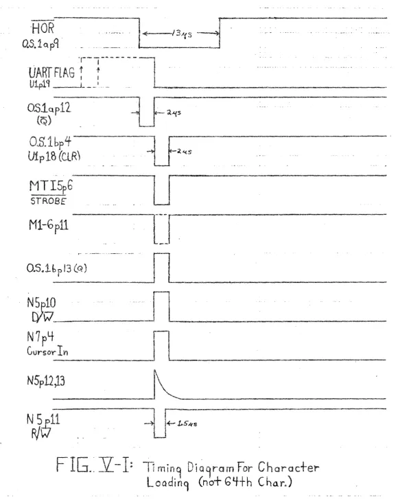
V-I: CHARACTER IDENTIFICATION
Character processinq is initiated when the HART flag (Ulp19) which is applied to OSlbp2 goes high to indicate receiption of a character*. On the next horizon-tal retrace pulse ~ goes low and nSla is triggered and
q
pin 12 goes low for 2us and is applied to OSlbpl. Since OSlbp2 is high, OSlb fires and OSlbp4 goeslow for 2us pullS MTI5p15 low, and resets the UART flag
hy
pull inCiUlp18 low. The most significant 5 bits (5 MSB's) of the ASCII character code are tied to pins 10 throuGh 14 of MTIS and the 2 lSP's (Least Significant Bits) are tied to A3pl and A3p6. MTI5 decodes the 5 MSB's to detect
if
the character is a displayahle or control character.V-2: DISPLAYABlE CHARACTER PROCESSING
If the received chay'acter is displayable ~1TI5 produces a STROS'r pulse at
pin
6 for the duration of nSlhls pulse (2us). ASCII data for the character is avail-able during the same 2us interval as follows:RIT
#
l(lSB)
at
A3p3 and Mlpl1 2at
A3p4 and M2pl13
at
~1TI5p4 and
M3pl1
*Please refer to Figure V-l.4 at MTI5p3 ~nd M4pl1
5
at
MTI5p2 and M5pl1 6at
MTI5pl and M6pl1When a lower case alphabetic character
COdE
is received MTI5 and A3 produce the corresponding upper case code. The ASCII code set is given in Section IX of this manual.Since N5p9 is high N5pl0 goes high when StROBE falls (MTI5p6). The high level from N5pl0 is applied to pin 1 of Sl, S2 and 53 (the select line of the multiplexers for the 10 address lines to Ml through M7). This causes the three switches S1. 52 and 53 to allow C4 and C6 to address the memory. C4 holds the 4 bit address of the row that is presently being loaded (LA6 - LA9). C6 has the 6 bit address of the column into which the present character is to be loaded
(LA~ - LAS).
The rising edge of N5plO is capacitively coupled into N5p12.
13.
The capacitive coupling causes a 1.5us R/W (read/write) pulse at N5pl1 which drives theR/~
lines (p3) of Ml through M7. Hence the character is loaded into memory 1.5us after the lJART flag and 'ffi'JI'f coincide at 051b.The rising edge of STRO~E (MTI5p6) causes a falling edge at N5pl0~ C6pl and 51, 52 and S3pl. This falling edge increments C6 and returns control of the RAM address lines to the display circuitry.
Whenever a displayable character is loaded C6p3(Q6) ;s low and hence M7pl1 (cursor bit into memory) is high and a 1 is loaded into the cursor bit for the position which is being filled.
When a character is loaded into the 64th column a scroll operation is initiated
by
virtue of C6p3(Q6) going high. The scroll operation is described in Section V-4.---'
'HOR
QS~1o.pq
~tN~lAG
rJ··----lu
_.
.
Ml-Gpll
=-MTI5pb
STROBE'
O.slQP12
(Q)
O,S.1bp4
Vip 18
(ClR)
..
_--~
l
F
a.A(Sl
[~~S
.
-
,~ .~.-U
~~f
,--
-~
0.5..1
b
0
i
13
(Q )
"'.•... "
--
..•.NJ~=ll
_. _.
_
N7pLf
[image:24.627.42.623.37.765.2]Cursor
IYI
FIG ..}l- 1:
Ti
min9
DiQ9ram For Character
Loadin9
(hot
GY-th
CharJ
V-3: CR PROCESSING
When A CR (Code 00 Hex) is received
by
the UART MIlS produces a 2usec low pulse at pin 7 (~ which is inverted and applied to FF3ap6 (set input of CR FF)0 Please refer to FigG V-2w When the ~ line falls the CR FF is set and FF3ap2 (~ falls -- initiating the CR process@Since MIlS decodes only the 5 MSB's of the ASCII character code
it
produces a ~ pulse for four ASCII codes;iee.,
OC-Form Feed; OC-CR: DE-SO and OF-ST.To perform the CR function first the present row is filled with spaces and high cursor bits; then the pointer to the top row of the display (C4) has to be incremented modulo 16 and finally the bottom row of the display has to be erased. These last two actions comprise a scroll operation which is described in Section V-4.
The low level at FF3ap2 is applied to N5p2 which forces N5p3 and N5p6 high. The high at N5p6 enables a pulse train out of N5p4 as indicated in Fig. V-2.
Since N5p6 and N5p8 are high the pulse train from Nl0p3 is inverted twice and applied to C6pl~ Sl. 52 and S3pl. The Y'ising edge at NSp10 is capacitively coupled to N5p12t 13 to produce a 1.5us negative going R/V pulse at N5p'11 and Ml-M7p3.
O.S.1aplL) M T15p15
M TI SF 7 (CR)
Mn~ 6
(STROB~)
~I---~
-11 ••.•-2&$
lJr----~J
Blts~3,'1 HiS'"!
Ml-6pl1
toDE BIts').,5,0 L••w(R/Q)
NSpll
Ml-7f3
N
u-C
("J
r
I
tJ
/.J.J
::r
(/)
'-'
r-...::
'2
0
8
""
I .
H
c.ti
~
The fall"ing edge of pulses in the train applied to C6pl causes C6 to incre-ment each time a space is written into memory. When the 64th column is loaded
C6p3
rises.
The rising pulse resets the CR flip-flop (FF3a) and 1s inverted at N7p4 and applied to C4pi (Row counter) and increments C4 modulo 16. A scroll operation is performed next.
V-4:
SCROLL OPERATION
The scroll state (indicated
by
C6p3 going high) is entered to completethe CR operation.
N7p4 is low and applied to N5pl.
FF3ap2
(~
and N5p2 are
now
high
soN5p3
remains high and the pulse train continues to pass through N5p4. When the scroll state is entered as the result of C6 overflowing whileloading displayable characters (see last paragraph of Section V-2), N7p4
(~cro'T)
and N5plgo
low, FF3ap2 (~ and N5plare
high so N5p3goes
high and allows N5p4 to produce its pulse train which is used to clear the old top row of the display.Regardless of how the scroll state is entered, the high level at N5p3 enables a pulse train at N5p4 which is inverted once at N5pl0 (since N5p6 is
high --
SiR~~t).
These pulses are used to write spaces andl~
cursor bits intothe new bottom row of the display in exactly the same manner as they are used
to write
spaces
and .!!.!9.!lcursor bits
into
the memory for filling
~
i'OWwhich has
been terminated
by
a CRa Refer to Section V-3 for the details of how the new bottom row is cleared.When the memory location corresponding to the last (64th) column in the bottom (16th) row is cleared C6p3 falls, forcing N5p3 and N5p6 low~ The low level at N5p6 prevents any more pulses writing extra spaces into memory and incrementing C69
V-5: CLEAR (PAGE) OPERATION
The ACT-I screen clear function can be activated in two ways: 1) during the power-on sequence; and 2)
by
depressing PAGE key on the ACT-I keyboard.Automatic screen
clear
upon power-up is accomplished
by
coupling
the rising
+5 volt power supply through a 15uf capacitor and N7 to the set input of the CR
flip-flop
(FF3a).
The 5.61< resistor
discharges
the
15uf
capacitor
causing
the
set
input
to fall
after
approximately
50 milliseconds.
Depressing the PAGE key pulls N7pB low and forces N7plO and FF3ap6 (set) high. Hence th~ CR flip-flop is set for the duration that the PAGE key is depressed.
Holding FF3a in the set state causes the memory loading circuit to scroll repeatedly. Hence, all display memory positions are loaded with the ASCII space code and a low cursor bit. It takes only 40 milliseconds to clear the ACT-I screen"
If the PAGE
key
is depressed while characters are beinq receivedby
theHART
a
clear
screen
'v.dll
not always result
since
the c'lear
and load functions
were not designed
to operate
concurrently.
Programming Hint: In order to clear the ACT-I screen under program control (as opposed to manually depressing the PAGE key), a sequence of 16 carriage returns should be sent from the computer.
SECTION VI: OSCILLATORS AND CONTROL
The oscillators and control section (0
&
C) of the ACT-I is responsible for generating all timing clocks and control signals. The following components are used to produce these:Nl, N2. N3, N4. N8~ N9~ fII10,Al~ A2, A4, C7a, COD
C9t
ClOt FFlb, FF4a,b.VI-l: 9.B28MHz AND HORIZONTAL OSCILLATORS
All timinq signals in the ACT-I are derived from a maste~crystal-controlledg 9.828 Meqahertz, oscillator. The output of this oscillator at N2p3 drives a
divide-by-eiqht
cOI.,mter •.C9.•and also
feeds
N2p12 and Alp13.
~rhen N2p13 is
high
due to FFlb (nor-oscillatOr enaD'e) being in the reset state, the 9.828MHz square wave is gated throuqh N2pl1 to produce shift pulses for SRi. The inverted 9.828 MHz signal (N2p8) is applied to C1p1 and Alp9 in the video generator (Vr.) circuit.
The 1.2285
r~Hz
output
of C9 drives
the
lIART count
down chain
in the
input!
output section
(110)
and also provides the count in pulses for CiO which is adivide-by-79 counter.
The divide-by-79
is accomplished
by
lIandinq"the 00
(1-C10p12), Ql (2-Cl0pll). 02 (4-C10p9), Q3 (8-C10p6) and 05 (54-ClOp3) to gener-ate the reset input to Cl0 at A2p11. This output is high for the duration of the reset propagation delay of C10 (about lOOns). The short positive pulse at A2pl1
sets
FF4a (Hm'izontal
sync)
by
clocking
it
~rith
the D input
tied
high.
This short
pulse occurs every 64.3 microseconds (15.550KHz). When Cl0 reaches a count of
16 (13us after beinq reset) Q4 (C10p5) goes high and resets the horizontal sync flip-flop (FF4a). Hence the duration of the buffered Hor. sync and ~. ~ at N4p8 and Nlp3 respectively is 13us.
VI-2: LEFT MARGIN DELAY AND DOT OSCILLATOR ENABLE
04
of
C10
(p5)is
also applied to N3p12 to digitally control the left margin position. Hhen 04 and 02 of Cl0 both are high (20 counts after therese.t of
Cl0
and 4COU~t5
after the end of the horizontal sync pulse) N3pl1faHs
iind foy'ces N3p8
high"
The
rising
at N3pB
is
coupled
through
a 220pf
capacitor to N3p2. If the vertical pus; on of the beam is in the display area
(horizontal
scan lines
if,fjthrough
208)~ the
splay
Enable flip-flop
(FF'4b) will
be set and N3pl will be high so the positive pulse at N3p2 is inverted and causes
FFlb
to reset~
When the FFlb resets its ~ output (pin 8) rises and allows the9~828M!1zdot osci
11
a
tOY'to
ddve
the shi
ft
r'egi
steTSRl and the dot
C(H..mter
(Cl).
The output
of the dot oscillator
enable
f1ip~flop
(FFlbp8)
is gated with the
cursor data to the video combiner to prevent the cursor from being displayed
outside of the
splay area~
Q3 of Cl0 is used to increment C6 during the carriage return and scroll operations as explained in Section V.
VI-3: VERTICAL SYNC. AND DISPLAY ENABLE
The buffered horizontal sync pulses at N4p8 provide the increment siqnal to C8 which is a nine b'lt binary counter
(ca
is a modulo 260 counter). When C8 reaches a count of scan lines Q6 (64-C8p4) is high,Q]
(128-CBp13) is low. N9pl1 rises and clocks FF4b into the set state. FF4bp13(Q),
N3pl, A2p9and A2pl0 rise accordingly. A2plO is tied to the count-in line of C5. FF4b remains set until C7a reaches a count of 16 when the sixteenth row of characters finishes
being displayede
C7a is incremented each time the d1vide-by-ten displayable scan line counter (C3) resets. At the same instants positive going pulses are produced at A2pl0 to increment
C5
When CO reaches a count of 259 scan lines Q8 (256-C8p12)~ 00 (1-C8p9) and Ql (2-C8p7) rise9 forcing Nl0pl1 low resetting C8 and setting the vertical sync
flip-flop which
is actually two
ed nand gates
(N8p5~
694 and N10p8i 9, 10).
The output of this flip-flop is b~ffered through N4~
When C8 reaches a count of
4~ 02 (4-C8p6)
ses
and resets
vertical sync flip-flop.
Hence the duration
SECTION VII: VIDEO DISPLAY GENERATION
The most complex circuit in the ACT~I is the display generation circuit.
It
is
responsible for fetchinq characters
memory and generating the char~
acter and cursor da
for the composite video output si9nal.
The descri
on of this complicated circuit will start with the vertical
retrace pulse and proceed as the beam travels from the top to the bottom of the video frame. The follow1ng components are used to generate the d'isplay:
Nl~ N9, Al, A2, Cl-C3~ FF1. FF2~ ll, l2, CG1, SR1, 01 and 02.
In order
anhance your understandinq of the display
circuitrylsoperation
refer to Figures VII~l, VII-2 and VII-3.
At the top of the screen the vertical sync pulse has just completed and cleared C7a
(#
of character rows displayed), C3 (Modulo 10 scan line counter to address the character ~enerator chip) C8 (N of horizontal scan lines), and jammed the contents of C4 (pointer to bottom row of characters in memory) into C5 (character row address).Sixty-four zontal scan lines later C5p15 rises causing C5 to increment modulo 16. Hence the count in C5 changes from the address of the last row of characters (which was loaded into
it
hy
the vertical sync pulse at C5pl) to the address of the first row of characters to be displayed. The Disp. En. (FF4b) is set in coincidence with the end of the horizontal sync pulse since C8 counts on the rising edge of Hor sync.The trailinq edge of the Her sync is or-ed with Clp12
(lSB
of charactercol-umn counter) to produce the count in signal for C2 (which holds the second~ third~
fourth and fifth bits of the 6 bit character column address). Hence at the start of the first dispiayable scan line (line 64) and at all other scan lines from
64 to 224, the character column counter is initiated to a value of 2. The six column address lines can be located as follows:
I
i
, j
" i
.
I
11
r
.~I
'3'" •
U>
j
VII-2
~
&
~
il
I.
~
I
~
I
I
!
\
L
u:
!
- j
::r
:-
~
",g
-I~'
3
----I
I
.1
I
l
T
I
I
i
I
I
I
cn=
I
~.!!:-~
~
-~
u: -J
~-
~
_"J
Z
• ~"';:i
...>
..f.:
~
~w I...:.
..•. ..:
~ VI
""
'0
Ii..
.--
'"'"-u....P
0.... •.•
Q..
ro(!J
v ...•
c-!
VII-3
\
"'---
-,
V .-"~,
,-
---.
'hf
CJt,t\RAt.TERS
VII-4
<II> .0 ••• 0 II)
• ill' G' •
(/Ii ••• III •
••
.
••••
~
....
• 11 t> " •••
••••••
t
II"I #! SR}
!
\--2
"
3
.•..,.
t'
::J
6 (MS B)
location
Clp12
C2p12
C2p8
C2pil
FF2ap9
This column address is fed to the memory section through 51-53 and in com~
binathm
with
the
rO\'1address
count
held
in (;5
provides
the memory with
the
ad-dress of the third character to be displayed durinq the present scan line. Latch II contains the ASCII code for the second character to be displayed and the shift register
(SR1)
holds the dot pattern of the present character scan line (pointed toby C3)
of the first character to be displayed. latch l2a holds the cursor bit for the second character to be displayed and L2b holds the cursor bit for the character presently bein~ displayed.The
pul
SI? in amana nq from the dot oscillator drives Cl (dot counter and lSR of character column address), SRl (Shift register holding the dot patterns for the present character)~ and Alp12 (which gates the shift reqister data out to the video combiner circuit).On the rising edge of the dot oscillator pulses (N2p8) C1 increments. The serial output of SRip13 is anded with the dot oscillator pulses (N2p8) at Alpl0. This output p8) 1s anded with the delayed and inverted C3pl1 (MSB of the
character'
qenerator
scan line
address-counter).
Thus when the beam traverses
character scan lines eight and nine the serial data out of SRl is blocked at Alpl to avoid displaying erroneous dots during these two blank lines.
~!he!1Cl r'eaches
a count
of six
Nlp12 and 13 go
gh9
Nlpll
(II'~I)qoes
low~
and N1p5 ("6")
goes high.
The
1{
pul ses load the dot pattern
of the next
chi!U"acter
into
SRl
by
pulsing
SRlp15 low during
the
sixth
dot
of each
character
in a scan line.
The
"6il
pulses
are appH
to FFlapl
(C) to affect
the neqation
of the dot oscillator enable control signal when the 64th character has been displayed.
The risinQ edge of the seventh dot pulse causes the three least significant
bi
ts of
C'1
to
tmesetto zero
whi
1e
the MSB increments
(toggl es) •
The MSBof
C1is the lSR of the character column counter. As mentioned above Clp12 (LSB col.
ent.)
and Hor sync.
are or-eo
into
C2p14 (count
in for upper bits
of char.
colo
cnt.).
C2
continues to count as the beam scans across the line and ~~I pulses are generated.When the character column count reaches a count of 64 FF2bp12
(0)
goeshigh9 removing the reset siqnal from FFlap2 and enabling FFla to toggle on the
faning
edge of the
11611pulses.
The
<routput
FFlap13
is
tied
to C3p14 (count
in line of the character scan line counter) so that C3 is incremented when the beam finishes displaying the 63rd character on the line and the 64th ~~9 pulse
will scan line data for the next line into SRl while the ASCII code for the second character in the next line is jammed into
ll.
The Q output of FFla is tied to FFlbp5 (clock line of the dot oscillator enable FF) and thus causes FFlbp8(Dot Oscillator Enable) to fall when the beam finishes displaying the 64th character. Since C3 is a modulo ten counter it increments C7a (Number of rows displayed)
and C5 (pointer
to present
rm;f) every 10 scan lines.
~""en
C7f! 't''i:'.achesa count
of
16
it
sends a capacitively coupled rising pulse into the reset pin of FF4b (Display Enable FF) causinq FF4p13(Q) to fall until the 64th scan line of the next frame when the entire process repeats.VIDEO COMBINER AND CURSOR GENERATION
Data shifted out of SR1~ cursor information and horizontal and vertical
video output signal which is capacitively coupled to the video out jack on the rear of the ACT-I cabinet. The output impedance is 1.2K.
The cursor data is generated by l2a, l2b and N9. When a negative goinq edge is sent from l2b to N9p8 through the R-C pulse circuit (which determines the width of the cursor), and C3pll (character scan line counter MSB) is high, a lus positive pulse will appear at N9plO and be summed into the video out signal causing a double underscore cursor to appear at the position into which the next character is to be loaded. When the cursor is in its home position it will not be displayed in order to avoid CRT burn in this heavily used position.
Positive Horizontal or Vertical sync pulses cause Ql to pull the video out signal into the blanking level for synchronizing the monitor.
SECTION VI II: TROllBLE SHOOTING
In order to pinpoint the faulty component in a malfunctioning ACT-I, the unit should be placed in the self test mode by choosing RS232C output and con-necting the serial out and serial in together.
Having placed your unit in the self test mode you are ready to determine which of the four major circuits is malfunctioning. These four circuits are:
1)
Power supply2)
Input/Output
3)
Memory loading
4)
Display
VIII-l: DISASSEMBLY
Performing the following tests requires access to the interior of the ACT-I cabinet. This can be accomplished by executing the following operations:
1) Unplug the ACT-I line and from its 110 volt AC source,
2) Remove the six "phillips" head screws which are located as indicated in the figure below (note that 4 of these are in rubber feet).
-0---0)
Bottom
1/
c
<.':> '//-_._--~/
3) Place the ACT-I in its upright position and separate the black bottom piece and the white top piece by lifting the front of the white piece from the black piece while holding the rear of both cabinet pieces in close proximity. The white piece should be lifted to a vertical position and propped as below to insure stability.
VIII-2:
EQUIPMENT
In order to perform the following tests the following equipment is required: 1) 35 MHz oscilloscope with dual trace
2)
voltmeter
3} phillips head screw driver
VIII-3:
POWER SUPPLY TEST
With the ACT-I turned on measure the +5 volt and the -12 volt power supplies on the main circuit board. The +5 surply can be found at the rightmost pin of the three 7805 regulator pins. The middle pin should b~ grounded and the left-most pin should have about +17 volts with about one volt of ripple. The 7805
(plus 5 volt) regulator should be securely fastened to the ACT-I chassis in order to heat sink
it.
The minus twelve volt supply can be iDeated at the emitter lead (rightmost) of the MPS3638 pass transistor (03). Minus 12 can be ~und on the main circuit baord at pin 2 of the UART chip (Ulp2) and at pin 1 of the 2513 character gener-ator chip (CGlpl).
The +5 volt reQu1ator (7805) has short circuit and thermal protection and will shut off
if
its output gets shorted orif
it
gets too hot. A thermal problemwin
cause the output
to cycle
on and off as the chip's
temperature
changes.
Proper
heat sinkinq of the regulator to the ACT-I chassis will prevent any thermal problems. The -12 volt supply is a zener diode-pass transistor type. It has no short circuit or thermal protection. Should its output become shorted the MPS 3638 pass
trans; stor
win
be permanently
damaged.
Under normal operatinG
conditions
the
-12 supply is loaded very liQhtly and the ~1SP3638 needs no heat sink.
VIII-4: DIAGNOSIS OF MAIN BOARD ~1AlFUNCTIONS
Havin~ determined that the main board is a fault you can determine which of
the I/O, memory
loadinQt
or display
circuits
is faulty
by
performing
the followinq
tests.
VIII-4.1: I/O TEST
With the unit in the self test mode (described at the beginning of this section) repeatedly strike the letter A and compare actual waveforms with those g'iven in section III of this manual. If the necessary signals check out and in particular
if
the negative going pulse(STROSr)
appears at pin 6 ofriTI5 and the UART clock frequency is correct. the
1/0
circuitry ;s performing as requiVIII-4.2:
MEMORY LOADING TEST
Depress the PAGE key and verify that FF3a (CR FF) sets and remains
set while the PAGE key is depressed. Also verify that C6 and C4 are counting properly and
R/\~
pulses appear at Ml-M7p3 as described in section V. If these waveforms check out the memory loading circuitry is not at fault.VIII-4.3:
MEMORY TEST
The most common memory failure is a tendency to make bit errors. For
examrle after clearing the screen an ~ may appear in one position on the screen. This is due to an errant memory bit in the least significant position (ASCII code
for space = 2016' ~ : 2116), If this problem occurs the appropriate memory
(Ml-M7) should be replaced. Another symptom is that when loading a given position with a character the character in a different position is altered. The bit which is modified indicates the faulty memory chip.
VIII-4.4:
DISPLAY GENERATION TEST
If the power supply I/O and display loading circuits pass their tests and an abnormal display (or no display at all) persists the display circuitry is at fault. Refer to section VIr and verify that all waveforms are as indicated.
Some s.vmptoms and the associated remedies are listed below:
VIII-5: TROlJBLE SYMPTOMS AND REMEDIES
The following is a list of reported trouble symptoms and the remedies suggested by the Micro-Term technical staff:
SYMPTOM
1) Rubout code (FF Hex) sent instead of struck character
REMEDY
SECTION IX: TECHNICAL INFORMATION
IX-l :
ASCII CODES
HEX
CHAR
HEX
CHAR
CHAR
HEX
HEX
CHAR
CODE
CODE
CODE
CODE
00
NUL
20
SP
40
@60
01
SOH
21
!
41
61
aA
02
STX
22
"
42
B62
b
03
ETX23
If43
C63
c
04
EOT
24
$
44
D
64
d
05
ENQ
25
%45
E65
e
06
ACK
26
&
46
F66
f
07
BEL
27
,
47
67
G908
BS
28
(48
H
68
h
09
HT
29
)49
I
69
OA
IF
2A
*
4A
J
JGA
08
VT
28
+
48
K
68
kOC
FF
2C
,
4C
L
BCI00
CR
20
-40
M
60
m
DE
SO
2E
N
4E
6E
n OF SI2F
I
4F
0
6F
0
10
OLE30
0
P
P50
70
11
DCl
31
151
Qq
71
12
DC2
32
72
r
2
52
R
13
OC3
33
3
Ss
53
73
14
DC4
34
4
T
t
54
74
15
NAK
35
5
55
75
u
U
16
SYN
v36
6
7656
V
17
ETB
37
57
Ww
777
18
CAN
38
8
X
x58
78
19
EM
39
9
59
Y
Y79
1A
SUB
Z
z3A
7A
5A
1B
ESC
38
,
58
[
78
{
1C
FS
3C
<
\
I
7C
5C
10
GS
30
=:7D
50
]
}
1E
RS
3E
>
5E
1\
7E
IF
VS
3F
5F
?~DEL
7F
IX-2 GENERAL SPECIFICATIONS
~isp'lay (Receiver]:
Format - 64 characters
by
16 linesSpacing ~ Horizontal - one dot between characters
Vert'ical - 3 scan 1 ines between rows of characters
Character set - Uppercase alphabet, numbers and punctuation; 64 total ASCII codes
Refresh rate - 60 Hz (non-interleaved) Video out - 1.5 vp-p, RS 170
Cursor - Underline, double stroke, extinguished in home position to prevent phosphor burn and prolong CRT life
Data Rate - the display (receiver) can load characters at rates between 110 and 9600 Baud, RS232C or 20 ma current loop
Transmitter:
Character set - uppercase ASCII - includes all control codes Data Rate - 110 to 9600 Baud crystal controlled - RS232C or 20 ma
current loop
General:
Power - 110 volts AC, 50-60 Hz, 15 watts Size - 7.5 x 36 x 28 em (3 x 14 x 11 inches) Weight - 5 Kg (8 lbs.)
IX-3:
INTEGRATED CIRCUIT IDENTIFICATION AND POWER CONNECTION = REV. C+5
Ground
Part
I~
Pin
Piri
Other Power Pin(~
---Al, A5 74lS0B14
1
A2, A34081
14
1
A4
4082
14
7
Cl 74925
iO C2 74-935
10
C3
7490
510
C4,C6,Cl04024
14
7
C5
4029
16
8
C7
4520
16
8
ca,en
404016
8
C9
7493
510
CG2513
24
10
-5v pin 12. -12v pin 1FFl,FF2
74LS73
4
11
FF3,FF44013
14
7
U
74lS174
16
8
l2
74lS7414
7
Ml-M721 0211 PC
10
9
Nl,N3,N4 74lS0014
7
N2 740014
7 N5,N7,N8,Nl0 401114
7
N94001
14
700S~
1
74123
16
8
OPl MC14588
_<W:I> -12v pin 4
Sl-3
74lS15716
8
SRl74166
16
8
!J1A,,{-5-1013
1
0[!J
(
-~.
~
~
a::
Z
4:
<f) •
0-GI
<r4
~
~
~GJ[E]
00 [E]
u
To 33
(M)
LA'J \
~lAe.
--) lltt7
...•LAb
i 'I
----) T@ Sf• QlW"1"1)Stpj~S3e1(M')
~LAS
~To
52 (M)
C G Q~
t•••.
1!5~02't~ '
LA3r
lit
<'tt"l LA2. ToS1CM)Q,/I
LA1-Qo 11 LA"
R <4
:iI3
lOt
I
~Ol~
ic
11"
5' 16A L-(FROM ClOp'
fROM N'4p~ (o4~)
(o4.t)
~.
'-+5-1 IV? ,-1./
~
-I'&.
Q
~
If
t-.-';nplb
"ClEAR"
5'.'-" .•S'
~!
QI!1
/0
N
+$
FRDM UART(u)
(I/o)
r--~
FRoM UplO(II
0)Up9
)---...!!..
upa~
Up7' 13
Up6
Upl'b----,
X
I"
I
I )f'l~
I
W '" uplg~
6
?
Mb~~() ~
FRO M
115i
'(
WLI
2Q S"fv1
E
M 0 Ry ~;~
I 07'1!1J17Q 'IQ10~E('
Ti
ON
/3c"" r:f\/2.U '"' I M3r~-'<I >Qf
(M)
MlIh-~
CD bQI~
. P 1
Mlp 3 III I~
~L-.
!
Q~
's#
~ 'iL"-,.'hbEC
-:=jW-' Oifr
~I'LI(
r\.. F\.
I
19t1
r'+rU-VfRT. SYNC.-r~O<1(0,"NIP\-~OA.C.d SV.IC.
VIDEO
I
-+5C.OMBINER.
+S
f'ROM.N1.pll
(ot~)
-I-S-f){ThSH
D
P.
r
SRi
1/ F
7~lbb
Qul13
12-G
(If I-!
A!II111./ ~R
~~~R
C3-7'fQO
2. IS"
9D Lh
Q~Ie.!.'l'fL571/2.
CURSOR BiT
!'lor;
MY!
(M )
X
t
~
FROM ~J2.I>B
(o~c )
r--'~-lq
IIltLU
Q
iNLS7'1
+!;
+5
10
~
~~.rf'<.()M
(ote)
FFlbf'O+5"
••
Q,~Q-z.::' MPS5172
./
HOR'SYNC To C.lp'i)CHOR
2. 1
p ANb VIDEO CoM8INE!\TaOSIP'!}'1 ~ (VG-) +1;
AS & AND Ff2.pZ.1G
(J
(IJo,VO)NI
i~F
1..10lI._
~ To CII(r/o)r1D
:roA1p'f (V.GJ,
Nit
pS(v.G.)q
To CSpl5'
(L)
f.E'0T2. /I I
-13
5
NifI
ToANti C3p3(v&)VIDEOC.olleIIlEI'. (V(1a:SI'IoIC;)10
To C5'pl(L)
'/
I
ifN3'
3O~~·
"',
f
~o..n:c
7a.1't520
~S"
~() FF'tb 13
101\t'lCI'~ Q G7¥
II DIS/\£N.
~'ii
FF+5'
Cd
II
CP
I
t
9-
74
9 3
CIO-lf021f
~'!(L)
x
,
t".,
..
RC.VR DATA
To
MEM. LoAf!
(L)
- -7,
I\S2'32. c."" \I
-' Loot' P
Q,p
MP55' I? 2.
Qj
MPS3638
IGOJ'l /J "
loop 1\1
"OUT'"
lie.
C7b-t!f520
_~ RCVRFlAG-
To
o.s.1bp2. (L)<FMM o.'3.1bpl.f (L) CLEAR FLA&.
--:" MTI5pto --- M1I5
r
({7
MTI5'r 12~ MT1SpI3
~MT15'rl4
~To
A5pl
~To A3pb
.J
11K '4800'
1
"
12. 1'101
C11-
LjOLjO 18Ul
t;
A¥5-1015 ~ a I~K _ll-r---:1~
~
30;!.
UI
?:1lb
2.2.1{ 4~ FROM>--~c.
C'Irll
(a~t)
l.22BMH"2: 5.(,1( 4$' 5-'k"B~eQk'\ ,"
~ 'BreaK \I.e
V l'Ie:;j' .
¥
\lpi
To T:tp ~ S01AL OIlT
OF/~£R."t)uT" J1r? ~
ON REAR OF CASE:
"J1'1
CAS£:
'V
(KP9 ~~ "IJ'GROUND 1.:" JI,.!3 ;
1",0/,\ (Kp13 >-=:_'_
KE'r'Bol>.'U<;
(I<)
I k
Kpl1If~J!.
~'t!<~b~
Krll ) TIf'U
I<I'~~'
kplO ~2.
.,kfl4 )-Jlpl't . "1:" "':1::"
10 K8b {l<r1(K) "'r'S'
¢"rl!
(jlp1 -+5v12.v1(,5
nr3
t·"t
.p~,,<>'T• ~ - ~ '~IV . 0t7."_~~,,~ "1 , & " ••
I<
is
~TI>N7!J8 "t.;. '/:" _ INP ."PAG<;'" ' 8
(L) +5
",
" FROM fIr
0,:-S£P,.. IN" ON ~ SI!R!ALIN
REAR 01-" C.A5E' JlpS
X
I
0'1
--•.
8-1A0-I
-J,
3 '/ ••
(C2.,,11)(1'I'& <t)
-FRoM ~ P
'ac=
C~lOIl/JE'R (N5'p10j D/.\:7 ~~~
SECTION ( 'IV
-(l)
NSpl1)R/w
>-
-'.II
-.
_
POi
~
(L1p3)TO
I)O? (CUR SO'<) (L2(Lp'l)
DOG(Ll pG >
!
---J--
~--I
DOS-(l..1fLf ) +5SECTION
(l)
(A5fb)
PItt
M3
(A'Jf3)
(MTI'Sp1) (N7pl..;)DJ.5" J:rr6 I>I7
Y Y Y(CIlIUOI:.)
H
L
;t~
;1.
M5
~I
~j
2./0'J-j
M6Jj
1
M7
10'2.l
-1--+I-_J-jn·-1-1
j
,I
I
~
.
~== :~=J==~1J==~J
-J--
--I---j---j--j--
-L-~J--j
,--___
J
II
uj_
-_.
+5
LOADER
(A5p
8)
DI3
FROM
{!I3p
'f)
DI2 Y
M2
+s W D03 DOlt(LlpN)
(L.ip13)
(Llpl1)
V IOFO
GFNF
R
tiTCJR
{'VG \J_--
~---(/13p3) DT.1. +s .1' :1,AS __~ 11'13-
--5
'112--'-I'Ai-_
'C'IQ_ ~ 11 ---, DJ:Ml
.151'8 __ 2W2l.1 :1A-/11¥/ __ :1(;'1\7--L
q .12.DISI'I.AY AODRESS (DftNL/NtJi
O'M INATEIN V'DEO GENcR.Jm:;;R S€<:tJCJN (VG:: )
L(JI\~R AL!DRE$S (LA"",) L'N~S
OR'GIIVAT~ /IVU'N)ER SECTIOf'! (L.)
X
!
.. )(7
~
)(~ X'1_··X~
. '-Xl
IT~
Y.,pH
y
10P2.1Y,p2.'1 ysPB
~Z5
Ys-YSp26 Y.,pl?~~
(Ke!'1s",,·,+c.'k '5iJ.e) Y1pl'1 Y5PZ8
Y'p30
18
Tt ]
Y/31
Top'View
.
~
AY
5-2.376
EN
co
bER 1<1X3~f.,
Xl 37. X, 3~
~• 3'f
i1_lJ ••... ~ - •.. ~
SHII"'T"
n'J--H
\.L~
I
11."~RL~T~
J:ip'l
'i 5'
I~IC t5Y...A
X7,3lY
5
2
3
7
G k1 61 'J1.p 'n.r! ...-.~BI(e:AI\ CLEARnp16~_
,
{) I. 7 e,
10