ABSTRACT
This paper presents the design of an ultra low-voltage (ULV) pseudo operational transconductance amplifier (P-OTA) that is able to operate with a single supply voltage as low as 0.4 V. The proposed circuit is based on the bulk-driven technique and use of cross-coupled self-cascode pairs that boosts the differential DC gain. The stability condition of this structure for the DC gain is considered by definition of two coefficients to cancel out a controllable percentage of the denominator. This expression for stability condition yield optimized value for the DC gain. Also, as the principle of operation of the proposed technique relies on matching conditions, Monte Carlo analyzes are considered to study of the behavior of the proposed circuit against mismatches. The designed P-OTA have a DC gain of 64 dB, 212 KHz unity gain bandwidth, 57˚ phase margin that is loaded by 10 pF differential capacitive loads, while consume only 16 µW. Eventually, from the proposed P-OTA, a low-power Sample and Hold (S/H) circuit with sampling frequency of 10 KS/s has been designed and simulated. The correct functionality for this configuration is verified from –30˚C to 70˚C. The simulated data presented is obtained using the HSPICE Environment and is valid for the 90 nm triple-well CMOS proc- ess.
Keywords: Pseudo Operational Transconductance Amplifier (P-OTA); Bulk-Input; Ultra Low-Voltage (ULV); Sample
and Hold (S/H) Circuit
1. Introduction
The ultra low-voltage (ULV) supplies available in mod- ern CMOS processes are a challenging matter for analog designers, and operation of ULV analog circuits has be- come inevitable due to scaling down of semiconductor technology [1-3]. This is evident from the International Technology Roadmap for Semiconductors (ITRS) [4]. This requires traditional circuit solutions to be replaced by new approaches to circuit design and more flexible structure strategies that are compatible with future stan- dard CMOS technology trends. This is especially true for very high integration levels and very large scale inte- grated (VLSI) mixed-signal chips and SOCs. In mixed- signal systems, the analog circuits are combined with digital circuits in order to get the best performance with a low-voltage supply and low-power consumption. This combination should be done in an optimal way and the optimization process is application dependent. Recently, it has been possible to design circuits using power sup- plies as low as 1 V, and fabricated in the CMOS 90 nm
technology. So far, CMOS 22 nm technology products will be available in the year 2013 with a power supply of 0.5 V [1]. While the supply voltage applicable in deep sub-submicron design will continue to decrease and eventually fall below 1 V, the threshold voltage will re- main relative stable close to 250 mV [5-7]. This problem is mangified due to the fact that the threshold voltage (Vth)
never decreases linearly with decreases in the power supply. There are a number of techniques for ultra low-voltage circuits such as use of self-cascode MOS- FETs and cross-coupled pairs were proposed [1,2,8]. Meanwhile, self-cascode configuration connects the gates of two transistors together and provides high impedance with larger voltage headroom than the conventional cas- code structure. The output resistance is roughly propor- tional to the transistors’ dimensions and the effective voltage is the same as in a single MOSFET. Also, the bulk-input technique [9-14] shows a superior perform- ance, which allows for operation in the moderate inver- sion region at supply voltages equal to the Vth of the
technology. This technique, which uses the bulk terminal as signal input, is a promising method as it achieves en- hanced performance without having to modify the exist- *Corresponding author.
ing structure of the MOSFET [9-15]. Furthermore, the bulk-driven technique has better linearity and smaller power supply requirements. For a traditional MOSFET, the voltage applied to the bulk actually reduces the threshold voltage of the transistor, which increases the inversion level [16,17]. When applying this technique in circuit design, satisfactory performance can be achieved especially in ULV and low-power applications. OTAs are the key active building blocks of analog circuits. Fully differential OTAs are preferred because they pro- vide larger signal swing, better distortion performance, better CM noise and supply noise rejection, but a CM feedback (CMFB) circuit must be added [18]. Also, fully differential OTAs work very well and can substantially improve the system’s quality, especially in very un- friendly environments such as mixed-mode applications. However, at lower supply voltages, Pseudo OTAs (P- OTAs) could be used to avoid the voltage drop across the tail current source used in the fully differential structures. Various designs have been reported in the literature [1,8,16]. This paper presents the design of an ULV bulk-driven P-OTA in 90 nm triple-well CMOS tech- nology with supply voltage as low as 0.4 V. As the prin- ciple of operation of the proposed technique relies on matching conditions, Monte Carlo analysis and Process- Voltage-Temperature (PVT) tests are considered to study of the behavior of the proposed circuit against mis- matches. Eventually, from the proposed P-OTA, a low- power Sample and Hold (S/H) circuit has been designed and simulated. The design procedures of this structure are organized as follows. Sections 2.1 and 2.2 presents and analyses the small signal of the main P-OTA. In Sec-tions 2.3 and 2.4 the bias circuit and CMFB structure are reviewed. Then S/H circuit is introduced in Section 2.5. Section 3 presents simulation results. Finally, the conclu-sion is given in Section 4. The Appendix gives details of the analysis.
2. Bulk-Input OTA Circuit Design
2.1. Main Amplifier Circuit
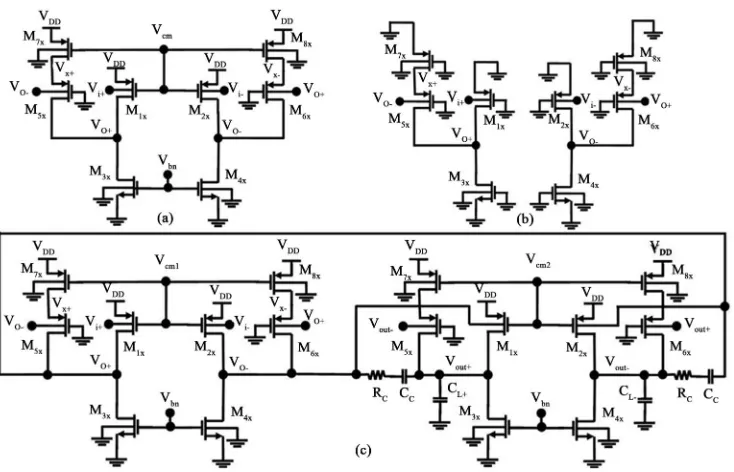
A very low-voltage bulk-input P-OTA without bias and CMFB circuits is shown in Figure 1(a). Also, for small
signal analysis, the AC model of this configuration is depicted in Figure 1(b). In this structure, a PMOS P-
OTA is implemented due to the action of M1x, M2x, M3x
and M4x. The two inputs are on the bodies of PMOS tran-
sistors M1x and M2x and the body transconductance of
these devices provides the input transconductance. These devices are loaded by the NMOS transistors M3x and M4x,
which act as current sources. To further improve the dif- ferential gain, PMOS devices (M5x, M6x and M7x, M8x) are
added. This configuration is a cross-coupled cascode pair that adds a negative resistance to the output and boosts the differential DC gain [19]. In this structure, the gate
inputs of transistors M5x and M6xare biased at zero due to
the limitation of the power supply voltage. Also, the gate inputs of M7x and M8x are connected to the gates of input
transistors M1x and M2x and biased at 100 mV, which
biases them in moderate inversion. Forward biasing of the body-source junction has been applied in low-voltage digital circuits [20-23] and it is applied here to lower the
Vth of the transistors. We typically apply a forward bias
up to 400 mV of VDD, which results in a lowering of the
Vth by about 50 mV. In the context of 0.4 V operation,
the risk of forward biasing the junctions is minimized since parasitic bipolar devices cannot be activated even when the full power supply is used as forward bias. In addition, to obtain adequate gain, identical gain stages can be cascaded so that a two-stage P-OTA is obtained as shown in Figure 1(c). In conclusion, the P-OTA is stabi-
lized by adding Miller compensation capacitors Cc with
series resistors Rc for right half-plane zero cancellation.
In the designed P-OTA, Cc = 2.6 pF and Rc = 50 kΩ are
assumed, respectively.
2.2. Small Signal Analysis
The drain-to-source accurrents of an NMOS and a PMOS transistor are given by
ds m gs mb bs ds ds
i g v g v g v (1)
sd m sg mb sb ds sd
i g v g v g v
i i
v v
(2)
where gm, gmb, and gds are the gate transconductance, bulk transconductance, and output conductance, respec- tively. Then, using (1) and (2) and considering
and vovo
, we have
1
1 4 7
mb v
ds ds ds
g A
g g g
(3)
5 55 55 7
mb ds
m mb ds ds
g g
g g g g
(4)
As can be seen from Equation (3) the conductance of
7
ds
g
can be used to boost the gain of the P-OTA.
Identically, we define coefficients of and
margi due to process and temperature variations so that
their ds7
0 1
n g
g
term cancels out only percent of the denominator. According to the above statement we can obtain the first stability conditions as follows:
gtotalgds1gds3 gds7 gmargin 0 (5)margin total,0 1
g
g (6)
total total 1 total 0
g g g
(7)Then the maximum gain will be given by
1 1
total margin
mb mb
vMax
g g
A
g g
CS Figure 1. Proposed P-OTA: (a) One stage of the P-OTA; (b) AC model of the P-OTA; (c) Two-stage P-OTA with miller com-pensations.
We know that 0 1
7 0
ds g
; then
gtotal gds1 gds3 (9)5 5
1 3
5 5 5 7
mb ds ds ds
m mb ds
7 0
ds ds
g g g
g g g g
0
g g
(10)
We know that for boost, the gain must satisfy . Therefore, the stability conditions for this structure can be expressed as:
[image:3.595.317.526.359.452.2]
g g gmb5gds5,7
Figure 2. CMFB circuit used in reference [6] and proposed P-OTA.
1 3
ds ds (11)
output of the second stage. Therefore, two independent feedback circuits are needed to establish the CM voltage at outputs of the first and second stages. This structure uses four PMOS transistors, Mc1 - Mc4, and two NMOS
transistors, Mc5 and Mc6 in the first and second stages,
respectively. The NMOS device is a bulk-input current mirror which compares the currents of the PMOS devices and then the difference between these currents is fed to the gate of the input transistors (Vcm1 and Vcm2) to control
the output CM voltages. This structure is able to operate with a ULV as low as 0.4 V.
2.3. Common-Mode Feedback Circuit
Fully differential OTAs require a Common-Mode Feed- back (CMFB) circuit. This circuit should behave linearly and only respond to CM voltage. A lack of this feature causes the Total Harmonic Distortion (THD) of the circuit to increase. Furthermore, a CMFB circuit amplifies the difference between the average of Vo+ and Vo-, and sends a
feedback signal Vcm to set the bias voltage at the gates of
the input transistors of the OTA. Nowadays, designing a CMFB circuit which is able to operate under a ULV sup- ply is very difficult, mainly because of the difficulty of detecting the CM voltage. In Reference [16] a CMFB circuit was designed which operated at 0.5 V by using two resistors to sense the output CM levels. But this structure increases the die area and reduces the gain due to larger loads on the OTA. To overcome some of these problems, a CMFB circuit has been reported [8] which is used in this paper and is depicted in Figure 2. The CM
output voltage of first stage is not coupled to the CM
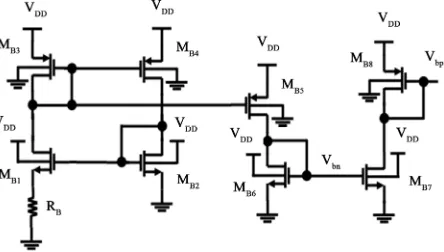
2.4. Bias Circuit
A low-sensitivity reference current generator and bias circuit are illustrated in Figure 3. Due to limited voltage
headroom, simple current mirrors are used to generate the bias voltages (Vbn and Vbp). Because the gate and
source of MB3 and MB4 are common for both transistors,
and the aspect ratios are equal, IDMB3 IDMB4
2 1 1
.
Copyright © 2013 SciRes.
B3
MB2 DM
B3
MB2I I
K W L
3
2 2
B
DM
n ox n ox
B DM
C W L C
R I
(12)
In the above mentioned equation, K is the ratio be- tween the aspect ratios of MB1 and MB2. Rearranging this
expression,
3 2
1 2
B
DM
n ox B I
C K W
R
2
2
1 1 B
M
L K
(13)
In the target circuit, K = 1.25 and RB = 1 k, and thus a
low sensitivity supply voltage independent reference current circuit is also designed and simulated which gen- erates a stable 1 μA reference current for the bias circuit. As expected, the circuit is independent of the supply voltage. Transistor MB5 mirrors this current to generate a
stable 1 μA reference current, which is used in the bias- ing of PMOS devices. In order to ensure that all the tran- sistors operate in the saturation region, bias voltages Vbn
and Vbp are applied to the gates of the NMOS and PMOS
devices respectively in the P-OTA and CMFB circuits. These bias voltages have been tested versus temperature and power supply variations. For –30˚C to 70˚C tem- perature range and power supply variations of ±6.25%, the sensitivities of these voltages are about 0.24 mV/˚C and 0.33 mV/˚C, respectively.
2.5. Sample and Hold (S/H) Circuit
The in this section, the whole S/H circuit is introduced. The proposed structure has been implemented using CMOS 90 nm technology and simulated in Hspice Envi- ronment. Figure 4 shows the entire S/H circuit. This cir-
cuit uses a two-phase, non-overlapping clock configure- tion. Here, ϕ1 and ϕ2 are the non-overlapping clocks. The sampling frequency is 10 KS/s. During ϕ1 the input signal is sampled differentially, while during phase ϕ2 the P-OTA is put into a unity gain configuration.
For a power supply voltage of 0.4 V, and Vth≈ 0.4 V a
[image:4.595.319.528.83.186.2]transmission gate switch could possibly be used. How- ever, the source of the switching transistor can be at a
Figure 3. Reference current generator and bias circuit.
1 f C
L
C
Vin+
Vin - Vi+
Vi
-Vcmi Vcmi
S
C
L
C
2
S
C
2 f C
Vo+
Vo -Vcmo
1
1
2
2
1 2 1
1
1
1
2
Figure 4. Sample and hold circuit.
very different voltage from the substrate, so the device threshold voltages can vary over the possible signal range [24] for typical process parameters. The well- known approach is use of Switched OTA circuits [25]. However, implementation of S/H using the switched OTA technique is impossible, while the circuits such as pipelined ADC converters require S/H operation at the input. Other approaches to overcome this problem are to use internal voltage boosting [26-32] that is used here. In voltage boosting techniques, some cases the clock volt- age is doubled, and that can lead to reliability issues.
3. Simulation Results
Based on the analytical procedure described in the pre- vious sections, a new ULV P-OTA was designed at a single supply voltage of 0.4 V from a 90 nm triple-well CMOS process and then simulated by HSPICE. The threshold voltages of this technology for NMOS and PMOS transistors are 0.42 V and –0.43 V, respectively. Then, from designed P-OTA, an ULV and low-power S/H circuit has been implemented.
3.1. Frequency and Transient Responses
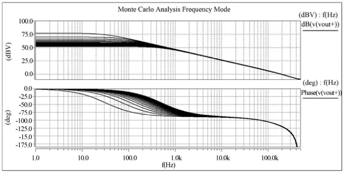
The open-loop frequency response and closed-loop tran- sient response of the P-OTA were tested. For a CM input of 200 mV, a DC gain of 64 dB, a bandwidth of 212 KHZ and a phase margin of 57˚ were obtained. Figure 5
shows the frequency response of P-OTA. Also, to exam- ine the effect of the doublet on the circuits’ settling be- haviors; the P-OTA was configured as closed-loop unity- gain amplifiers with 0.2 pF capacitors.
Then a 200 mV input CM voltage and a 100 mV step were applied to the P-OTA’s input, and then output voltage with 1% error was observed. In this state, the output voltage settled to its final value in less than 4 µs for rising time and 3.3 µs for falling time, respectively.
Figure 6 shows the step responses of the P-OTA.
3.2. Monte Carlo Analyzes
[image:4.595.62.284.593.719.2]Copyright © 2013 SciRes. CS Figure 5. Frequency response of proposed P-OTA.
Figure 6. Settling simulated results of proposed P-OTA.
Figure 7. Monte carlo frequency analysis of proposed P-OTA.
Carlo analyzes of the P-OTA in frequency and transient modes. The result shows that the amplitude and the phase were almost independent of circuit parameters.
Also, in transient test the responses do not have any
[image:5.595.128.469.490.660.2]3.3. Total Harmonic Distortion Response
The third obtained THD of the P-OTA, with a 200 mV amplitude and 500 Hz input frequency sampled at 10 KHz, were about 70 dB below the fundamental, as shown in Figure 9. It is obvious that the extra harmonics, but
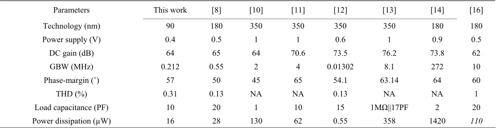
not the main harmonic have been eliminated. Finally, a comparison of proposed P-OTA with previous structures is summarized in Table 1.
3.4. Sample and Hold Output Responses
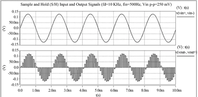
The input and output waveforms for a sinusoidal input of 200 mV peak-to-peak amplitude and 500 Hz frequency with a 10 KHz clock is depicted in Figure 10. To evalu-
[image:6.595.129.469.200.367.2]ate the nonlinearity, SNR and SNDR for mentioned input signal were also calculated. The result as indicated in
Figure 11 exhibits higher than 57.9 dB SNR and 56 dB
[image:6.595.129.468.397.565.2]SNDR that corresponds to 9 effective bits resolution. The
Figure 8. Monte carlo transient analysis of proposed P-OTA.
[image:6.595.57.540.611.736.2]Figure 9. Total harmonic distortion of proposed P-OTA (Vinp-p = 200 mV, fin = 500 Hz, fs = 10 KS/s, np = 1024).
Table 1. Comparisons of characteristics of proposed P-OTAs with state-of-the-art P-OTAs.
[16] [14]
[13] [12]
[11] [10]
[8] This work Parameters
180 180
350 350
350 350
180 90
Technology (nm)
0.5 0.9
1 0.6
1 1
0.5 0.4
Power supply (V)
62 73.8
76.2 73.5
70.6 64
65 64
DC gain (dB)
10 272
8.1 0.01302
4 2
0.55 0.212
GBW (MHz)
60 64
63.14 54.1
65 45
50 57
Phase-margin (˚)
1 NA
NA 0.13
NA NA
0.13 0.31
THD (%)
20 2
1MΩ||17PF 15
10 1
20 10
Load capacitance (PF)
110
1420 358
0.55 62
130 28
Figure 10. S/H input and output waves (fin = 500 Hz, fs = 10 KS/s).
Figure 11. Total harmonic distortion of S/H (fin = 498.046875 Hz, fs = 10 KS/s, np = 1024).
Discrete Fourier Transform (DFT) of the data samples was also computed with the Hspice simulator. The result shows that the largest SPUR falls −57.16 dB below the RMS value of the fundamental corresponding to an SFDR of 57.16 dBc confirming the results obtained through nonlinearity evaluation.
4. Conclusion
A new bulk-driven pseudo OTA topology using of cross- coupled self-cascode pairs technique has been presented. The operation principle of proposed structure is based on modifying the effective conductance of the active loads and enhancing the effective transconductance. This structure has been simulated in the 90 nm triple-well CMOS process with a supply voltage as low as 0.4 V. The proposed cross-coupled self-cascode pairs add a negative resistance to the outputs of structure and boost the differential DC gain. Also, expression for the DC gain was given, which can be solved for the small signal analysis. Then, in this structure, the stability condition of the presented technique for the DC gain has been consid-
ered by definition of two coefficients to cancel out a con- trollable percentage of the denominator. This expression for stability condition yield optimized value for the DC gain. Besides, the exact expressions for the transfer func- tion coefficients presented in the Appendix were verified for a number of different sets of component values. The transfer function coefficients were calculated using the formulas in the Appendix, the poles and zero(s) were found by factoring the numerator and denominator of the transfer function, and those results were compared to the poles and zero(s) from a HSPICE [33] pole-zero analysis of the same small-signal circuit. For future work, the optimized parameters can be found using a Genetic Al- gorithm (GA) to get a high performance structure in analog integrated circuits. The P-OTA provides a DC gain of 64 dB, a phase margin of 57˚ and an open loop unity-gain frequency of 212 KHz with a 10 pF capacitive load. The total current of the P-OTA is 40 µA. In this design, the first and second stages consume about (1/3) and (2/3) of the total power consumption. Also, an output swing of ±0.12 V was obtained for proposed structure.
Furthermore, THDs of −70 dB was given for 200 mV amplitude and 500 Hz input frequency sampled at 10 KHz. In spite of the ULV, excellent supply rejections of 71 dB at 5 KHz was obtained. Also, a reasonable CM rejection ratio of 81 dB at same frequency was achieved. However, the smaller bulk transconductance and large capacitance from the body to the substrate, limit the bandwidth of the structures. Eventually, from the pro- posed P-OTA, a low-power S/H circuit with sampling frequency of 10 KS/s has been designed and simulated. In addition, the preliminary simulation results demon- strate the feasibility of the P-OTA for modern ULV and low-power mixed-signal chips and SOCs.
REFERENCES
[1] S. Chatterjee, Y. Tsvidis and P. Kinget, “Ultra-Low Volt-age Analog Integrated Circuits,” IEICE Transactions on Electronics, Vol. 89, No. 6, 2006, pp. 673-680.
[2] S. Yan and E. Sanchez-Sinencio, “Low-Voltage Analog Circuit Design Techniques: A Tutorial,” IEICE Transac-tions on Fundamentals of Electronics, Communications and Computer, Vol. 83, No. 2, 2000, pp. 179-196. [3] J. Ramirez-Angulo, R. G. Carvajal and A. Torralba, “Low
Supply Voltage High Performance CMOS Current Mirror with Low Input and Output Voltage Requirements,” IEEE Transactions on Circuits and Systems II: Express Briefs, Vol. 51, No. 3, 2004, pp. 124-129.
doi:10.1109/TCSII.2003.822429
[4] ITRS, “The International Technology Roadmap for Semi-conductors,” 2008. http://public.itrs.net
[5] Y. Berg and O. Mirmotahari, “Ultra Low-Voltage CMOS Current Mirrors,” Analog Integrated Circuits and Signal Processing, Vol. 68, No. 2, 2011, pp. 83-89.
[6] A. Baschirotto, V. Chironi, G. Cocciolo, S. D’Amico, M. De Matteis and P. Delizia, “Low Power Analog Design in Scaled Technologies,” Topical Workshop on Electronics for Particle Physics, Pairs, 21-25 September 2009, pp. 103-110.
[7] J. Pekarik, D. Greenberg, B. Jagannathan, R. Groves, J. R. Jones, R. Singh, A. Chinthakindi, X. Wang, M. Breit-wisch, D. Coolbaugh, P. Cottrell, J. Florkey, G. Freeman and R. Krishnasamy, “RFCMOS Technology from 0.25 nm to 65 nm: The State of the Art,” Proceedings of the IEEE Custom Integrated Circuits Conference, 3-6 Octo-ber 2004, pp. 217-224.
[8] M. Trakimas and S. Sonkusale, “A 0.5 V Bulk-Input OTA with Improved Common-Mode Feedback for Low- Frequency Filtering Applications,” Analog Integrated Circuits and Signal Processing, Vol. 59, No. 1, 2009, pp. 83-89. doi:10.1007/s10470-008-9236-z
[9] A. Guzinski, M. Bialko and J. C. Matheau, “Body-Driven Differential Amplifier for Application in Continous-Time Active-C Filter,” Proceedings of the European Confer-ence on Circuit Theory and Design, June 1987, pp. 315-319.
[10] G. Raikos and S. Vlassis, “Low-Voltage Bulk-Driven
Input Stage with Improved Transconductance,” Interna-tional Journal of Circuit Theory and Applications, Vol. 39, No. 3, 2011, pp. 327-339.
[11] J. M. Carrillo, G. Torelli and J. F. Duque-Carrillo, “Transconductance Enhancement in Bulk-Driven Input Stages and Its Applications,” Analog Integrated Circuits and Signal Processing, Vol. 68, No. 2, 2011, pp. 207-217. doi:10.1007/s10470-011-9603-z
[12] L. H. C. Ferreira, T. C. Pimenta and R. L. Moreno, “An Ultra-Low-Voltage Ultra-Low-Power CMOS Miller OTA with Rail-to-Rail Input/Output Swing,” IEEE Transac-tions on Circuits and Systems II: Express Briefs, Vol. 54, No. 10, 2007, pp. 843-847.
doi:10.1109/TCSII.2007.902216
[13] J. M. Carrillo, G. Torelli, R. Pérez-Aloe and J. F. Duque- Carrillo, “1-V Rail-to-Rail CMOS Opamp with Improved Bulk-Driven Input Stage,” IEEE Journal of Solid-State Circuits, Vol. 42, No. 3, 2007, pp. 508-517.
[14] H. Khameh and H. Shamsi, “A Sub-1 V High-Gain Two-Stage OTA Using Bulk-Driven and Positive Feed-back Techniques,” 5th European Conference on Circuits and Systems for Communications, Serbia, November 2010.
[15] Y. Tsividis, “Mixed Analog-Digital VLSI Devices and Technology,” World Scientific Publishing, Singapore City, 2002. doi:10.1142/9789812703842
[16] S. Chatterjee, Y. Tsvidis and P. Kinget, “0.5 V Analog Circuit Techniques and Their Application to OTA and Filter Design,” IEEE Journal of Solid State Circuits, Vol. 40, No. 12 , 2005, pp. 2373-2387.
doi:10.1109/JSSC.2005.856280
[17] C. Duan and M. Liu, “MOSFET Modeling for Analog IC Simulation under Ultra-Deep Submicron Technologies,”
Micro-Electronics Technology, 2006, pp. 205-209. [18] A. N. Mohieldin, “High Performance Continuous-Time
Filters for Information Transfer Systems,” Ph.D. Disser-tation, Department of Electrical Engineering, Texas A&M University, College Station, 2003.
[19] A. Ahmadpour, “A 0.4 V Bulk-Input Pseudo Amplifier in 90 nm CMOS Technology,” Proceeding of 13th IEEE International Symposium on Design and Diagnostics of Electronic Circuits and Systems, Vienna, 14-16 April 2010, pp. 301-304.
[20] M.-J. Chen, J.-S. Ho, T.-H. Huang, C.-H. Yang, Y.-N. Jou and T. Wu, “Back-Gate Forward Bias Method for Low-Voltage CMOS Digital Circuits,” IEEE Transac-tions on Electron Devices, Vol. 43, No. 6, 1996, pp. 904-910. doi:10.1109/16.502122
[21] S. Narendra, J. Tschanz, J. Hofsheier, B. Bloechel, S. Vangal, Y. Hoskote, S. Tang, D. Somasekhar, A. Kesha-varzi, V. Erraguntla, G. Dermer, N. Borkar, S. Borkar and V. De, “Ultra-Low Voltage Circuits and Processor in 180 nm to 90 nm Technologies with a Swapped-Body Biasing Technique,” IEEE International Digest of Technical Pa-pers. Solid-State Circuits Conference, Vol. 1, 2004, pp. 156-157.
Parame-Copyright © 2013 SciRes. CS proach to Realize Full CMOS Switched-Capacitor
Cir-cuits at Very Low Power-Supply Voltages,” IEEE Jour-nal of Solid-State Circuits, Vol. 29, No. 8, 1994, pp. 936-942. doi:10.1109/4.297698
[26] T. Cho and P. Gray, “A 10 b, 20 Msample/s, 35 mW, Pipeline A/D Converter,” IEEE Journal of Solid-State Circuits, Vol. 30, No. 3, 1995, pp. 166-172.
doi:10.1109/4.364429
[27] J.-T. Wu, Y.-H. Chang and K. L. Chang, “1.2 V CMOS Switched-Capacitor Circuits,” IEEE International Digest of Technical Papers. Solid-State Circuits Conference, San
Modulator with 88-dB Dynamic Range Using Local Switch Bootstrapping,” Proceedings of the IEEE Custom Integrated Circuits Conference, Orlando, 21-24 May 2000, pp. 13-16.
[32] U. Moon, G. Temes, E. Bidari, M. Keskin, L. Wu, J. Steensgaard and F. Maloberti, “Switched-Capacitor Cir-cuit Techniques in Submicron Low-Voltage CMOS,” 6th International Conference on VLSI and CAD, Seoul, 26-27 October 1999, pp. 349-358.
Appendix
In addition, the transfer function and pole zero (s) analy-sis of the small-signal circuit in Figure 1(c) is analyzed
here. With appropriate substitutions, the results of this analysis can be used for other related circuits in analog integrated circuit design. According to Equations of the first and second stages that is neglected here, a circuit model was obtained, which is shown in Figure A1. We
know that the poles in this structure can be real or com-plex, depending upon the element values.
However, real or complex non-dominant poles can occur in practice and can be calculated using the de-nominators’ roots from Equations in (A.12), using the exact transfer function coefficients presented in this pa-per.
Transfer Function Calculation
Writing KCL at the nodes Vx1,2, Vo+ and Vout− for the first
and second stages, yields
2 2 2 1
i Y v x Gvx2G v2 out (A.1)
2 2 1 2 out
x
v G GY v vout
(A.2) 2 1 2 G G Y 1 1 out i Y v
(A.3)
(A.4)
out
c o
Y v v
2 1 mb2 o
i i g v (A.5) Substituting (A.1) and (A.4) in (A.5) result in
2 2 2 1 2 mb c g Y Y G G Y 1 1 2 out ' 1 o c v v Y Y
(A.6)
In addition, for the first stage we have
2 2 x1 G v x G v o
i Y v (A.7)
2
1
1 2
x vo vo
G v
G Y
(A.8)
2 1 2 G G Y
1 1 o
i Y v
(A.9)
(A.10)
out
c o
Y v v
1
11 2
2
mb mb c v
c cs c cs c mb c
g g Y
A s
Y Y Y Y Y Y Y g Y
2 1 mb1 i
i i g v (A.11)
Substituting (A.7) and (A.10) into (A.11) yields
(A.12)
Pole-Zero Analysis
In this Section, to perfect the design in the first and sec-ond stages of P-OTA and pole and zero(s) analysis, we assume that 0
gmb5 gds5
and
0 g g
mb6 ds6 . So, from Equation (A.12) we ma-nipulate the desired P-OTA gain vout . The gain
transfer function is (see formula (A.13)), i
v assuming that 2 1 C mb R g
(A.14) 11 1 1
1 3
1
C C c o C C o
ds ds
R C C R C R C
g g
(A.15) 12 2 1
2 4
1
C C c o C C o
ds ds
R C C R C R C
g g
(A.16)
the approximate gain transfer function will be as follows
0 0 1 2 1 1 1 1 c v C mb A S A sC A S
S S
g
(A.17)
Rewriting (A.17), we obtain
0
2 0
1 2 1 2
1 1 1 c v C mb A S A s C A S S g (A.18)
Using (A.18), the poles and zero can be expressed as
1 1
c C C
z
R C
(A.19)
2
0 0
1 2 1 2 1 2
1 1 1,2 4 2 C C mb mb
C A C A
g g P 1
P P2
(A.20) Poles and will be real and widely spaced if
2 0
1 2 1 2
1 4 C mb C A g
(A.21)
Squaring both sides and rearranging yields
0
2 2 0
2 2
1
1 1
1 1 1
c c
C
c o c
mb
A S S
C A S
S S S
g
1 1
[image:10.595.61.546.283.660.2]Table A1. The exact expressions for the coefficients of the proposed P-OTA.
Definition of parameters Parameters
1 3 1
ds ds
g g S C
1
Y
7 2
ds g S C
2
Y
5 3 1 db db db C C
C
1 C 7 5 db gs C C 2 C
2 4 1 ds ds
g g S C
1
Y
8 2 ds
g S C
2
Y
L db db
db C C C
C 2 4 6
1 C 8 6 db gs C C 2 C 5 5 5 6
1 G gm gmb gds
G
5 6
1 G G
G
2 5 mb5 ds5
G Gg g
2 5 5
G GG
1 6 m6 mb6 ds6
G G g g g
1 6 6
G G G
2 6 mb6 ds6
GGg g
2 6 5
GGG
1
1
C C
R S C
c
Y
2 1 2
G GY
2 1 2
G GY
2 Y cs Y 2 Y cs Y
1 2 1 3 1 3
mb mb ds ds ds ds
g g g g g g
0
A
RC1gmb2CC
c
C C
R C
c
1 1 c o c
1
1 1
o R C
1
o
1
o C
R C
1
c
1
1 3 1 3 ds ds ds ds
g g r r
1 o R 2 2 c o c
2
2 1 o
R C
2 o
2
o C
R C
2
c
1
2 4 2 4 ds ds ds ds
g g r r
2 o
R
[image:11.595.61.285.156.225.2] [image:11.595.58.282.274.731.2]