ISSN Online: 2153-1293 ISSN Print: 2153-1285
A High Performance and Energy Efficient
Microprocessor with a Novel Restricted
Dynamically Reconfigurable Accelerator
Itaru Hida, Shinya Takamaeda-Yamazaki, Masayuki Ikebe, Masato Motomura, Tetsuya Asai
Graduate School of Information Science and Technology, Hokkaido University, Sapporo, Japan
Abstract
In the era of Internet of Things, the battery life of edge devices must be ex-tended for sensing connection to the Internet. We aim to reduce the power consumption of the microprocessor embedded in such devices by using a novel dynamically reconfigurable accelerator. Conventional microprocessors consume a large amount of power for memory access, in registers, and for the control of the processor itself rather than computation; this decreases the energy efficiency. Dynamically reconfigurable accelerators reduce such re-dundant power by computing in parallel on reconfigurable switches and processing element arrays (often consisting of an arithmetic logic unit (ALU) and registers). We propose a novel dynamically reconfigurable accelerator “DYNaSTA” composed of a dynamically reconfigurable data path and static ALU arrays. The static ALU arrays process instructions in parallel without registers and improve energy efficiency. The dynamically reconfigurable data path includes registers and many switches dynamically reconfigured to resolve operand dependencies between instructions mapped on the static ALU array, and forwards appropriate operands to the static ALU array. Therefore, the DYNaSTA accelerator has more flexibility while improving the energy effi-ciency compared with the conventional dynamically reconfigurable accelera-tors. We simulated the power consumption of the proposed DYNaSTA acce-lerator and measured the fabricated chip. As a result, the power consumption was reduced by 69% to 86%, and the energy efficiency improved 4.5 to 13 times compared to a general RISC microprocessor.
Keywords
Embedded Microprocessor, Reconfigurable, Low-Power, Accelerator, Digital Circuit, Architecture
How to cite this paper: Hida, I., Taka-maeda-Yamazaki, S., Ikebe, M., Motomura, M. and Asai, T. (2017) A High Performance and Energy Efficient Microprocessor with a Novel Restricted Dynamically Reconfigur-able Accelerator. Circuits and Systems, 8, 134-147.
https://doi.org/10.4236/cs.2017.85009
Received: April 2, 2017 Accepted: May 16, 2017 Published: May 19, 2017
Copyright © 2017 by authors and Scientific Research Publishing Inc. This work is licensed under the Creative Commons Attribution International License (CC BY 4.0).
I. Hida et al.
1. Introduction
The overwhelming trend toward Internet of Things explains why low-energy embedded microprocessors (EMPs) are becoming increasingly important. Sources of energy inefficiency in EMP architectures are fairly well understood: the need to 1) fetch/decode every instruction from memory; 2) write/read register files to acquire/store operands per every instruction, and 3) clock numerous numbers of F/Fs for pipelining multiple instructions on a data path. The power consumption generated by these factors is not directly involved in computation.
[image:2.595.261.489.578.713.2]Among the power consumption of general EMP, the proportion occupied by the ALU responsible for computation is approximately 10%, and the remaining 90% is occupied by redundant power irrelevant to computation (Figure 1). That is, by reducing such redundant power, we can improve the power efficiency of the EMP without degrading the computing performance. Thus, we may choose to “statically” map those instructions in heavily executed “recursive codes” to an array of ALUs prior to their execution. By running the codes only as combina-tory data paths with no registers, 1)-3) redundancies can be drastically reduced. Although this “reconfigurable accelerator” solution looks straightforward and attractive, there is an inherent drawback: it is hard to cope with complex control flows (i.e., lots of branches) typically in embedded applications, which explain why previous proposals have focused on simple code segments that do not have a branch. Green Droid [2] is a configurable processor for mobile devices with Android OS. The processor improves power efficiency by processing the hot path (most recursive code) of Android OS in hardware, but it has no versatility to other operating systems. ADRES [3] is a processor in which dynamically re-configurable function units (FU) are coupled to a very long instruction word (VLIW) processor. The processor improves performance by complementarily computing the hot path with the VLIW processor and FU array. However, the FU array cannot handle hot paths including multiple branch instructions, caus-ing a decrease in energy efficiency. CMA [4] is a reconfigurable processor with a processing element (PE) array consisting only of combinational circuits and it can be customized but cannot be dynamically reconfigured during execution. Therefore, although CMA is superior to conventional dynamically reconfigurable
processors such as MuCCRA [5] and DRP [6] in power consumption, it has low flexibility and requires an external controller in order to execute a large-scale program.
As mentioned example above, the conventional reconfigurable processor is unable to combine power efficiency and flexibility. Based on this observation, we recently proposed an abstract architecture for achieving both energy efficiency and versatility in control-rich embedded applications [7]. The architecture we proposed consists of a static arithmetic logic unit (ALU) array without registers and data paths that contains dynamically reconfigurable switches and registers, where the ALU array improves power efficiency and dynamically reconfigurable data paths ensure versatility. The contribution of this paper is to materialize the concept into executable micro-architecture, design/verify it in a silicon chip, and evaluate its energy efficiency.
In Section 2, we describe the architecture of the proposed DYNaSTA accele-rator. The accelerator consists of a static data path, a dynamically reconfigurable data path, and circuits for controlling them. In Section 3, we show the simula-tion results for the DYNaSTA accelerator and the measurement results of the fabricated chip. The processor with the DYNaSTA accelerator showed reduced power consumption by 69% to 86% compared to general processors. In Section 4, we will summarize the study.
2. Architecture
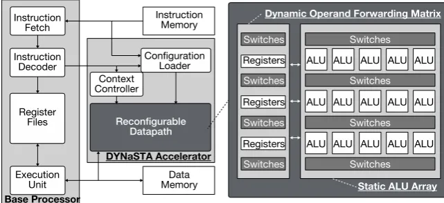
The key innovation in our proposal, a DYNaSTA reconfigurable accelerator, shown in Figure 2, is to combine two distinctive array structures different in nature, namely, a dynamic operand forwarding matrix (DYN) and a static ALU array (STA). STA computes an instruction sequence in parallel and plays a key role in achieving high-energy efficiency, where DYN is dynamically reconfigured while the accelerator is running and plays a key role to achieve versatility.
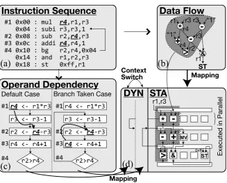
[image:3.595.210.531.555.702.2]The DYNaSTA accelerator executes instructions by the method shown in
Figure 3. When an instruction sequence to be executed by DYNaSTA is
ex-tracted, each instruction is mapped on the STA based on the data flow between
I. Hida et al.
Figure 3. Code mapping policy: (a) an example code, (b) extracted data flow, (c) ex-tracted operand dependency, and (d) mapping on DYN and STA.
the instructions, that is, the operand dependency, and the STA operates the in-structions in parallel. If the data flow changes during operation because of the execution of a branch instruction, the switches of DYN are dynamically recon-figured and an appropriate data flow is constructed.
In the following subsection, we will describe in detail the architecture of each circuit included in the DYNaSTA accelerator.
2.1. Static ALU Array
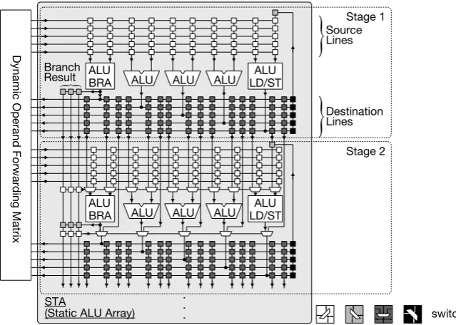
STA features a non-fixed number of stages, where each stage has several ALUs sharing a set of source/destination lines (Figure 4). To reduce the number of switches, hence improving energy efficiency, only parallel instructions are mapped onto a same stage, where branch/jump and load/store instructions go to the first and last ALUs, respectively (Figure 3(b) and Figure 3(d)). The instructions de-pendent on preceding ones are mapped onto the next stage. Conditional execu-tion is supported for discarding short forward branches. An appropriate number of STA stages is dependent on the sizes of the target codes, whereas that of ALUs per stage will range from 2 to 8, as in superscalar/VLIW architectures. Note there are no registers and hence no clocks in STA.
Figure 4. Block diagram of static ALU array (STA).
2.2. Dynamic Operand-Forwarding Matrix
DYN is a multi-context, bidirectional operand-forwarding matrix for solving this difficulty: it is dynamically reconfigured only when operand dependencies among instructions are altered on a branch (Figure 3(c) and Figure 3(d)). DYN is composed of temporary registers for storing operand values of each instruc-tion and a large number of switches, as shown in Figure 5. When the data flow of the program transits while the accelerator is running, the switches are dy-namically switched and appropriate data flow is constructed.
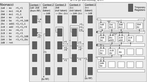
Figure 6 represents an example in which fibonacci, used as one of the
bench-mark programs in the evaluation, is mapped to DYNaSTA. In Figure 6, it is shown that the datapath on DYN changes according to each context, and the appropriate operands are forwarded to the STA. Keeping power-consuming dy-namic reconfiguration away from the massive ALU array (and leaving it static) is a key for achieving energy efficiency in DYNaSTA architecture.
2.3. Context Controller
The context controller shown in Figure 7 controls the transition of the context during execution. As the base processor starts executing the program, functions or subroutines processed by DYNaSTA are loaded from the instruction memory, and information of each context contained in them is stored in the configuration memory and the context memory. The context information is embedded in the executable file by recompiling the original executable file with the dedicated compiler; the function to be accelerated is also decided.
I. Hida et al.
Figure 5. Block diagram of dynamic operand- forwarding matrix (DYN).
[image:6.595.63.537.437.703.2]Figure 7. Block diagrams for configuration loader and context controller. DYN is dynamically reconfigured by these circuits.
results of the branch instruction and the delay of the previous context is equal to the value of the clock counter (meaning that the previous context has been properly executed), the next context configuration information is sent to DYN. After DYNaSTA finishes executing the function, the base processor resumes program execution from the address of the instruction memory specified by the return address.
2.4. Overall Architecture
We designed an EMP with this DYNaSTA accelerator into silicon (Figure 8). The base EMP is Mico32 [8], which is chosen because of its typical RISC archi-tecture and open-source RTL code. By treating “recursive codes” that are mapped onto DYNaSTA as subroutines, the read/write path between Mico32’s RF and DYN only needs to cover its arguments portion (four registers, Figure 8).
3. Evaluation
3.1. Instruction-Level Parallelism
Before simulating power consumption, we analyzed the optimal number of ALUs included in one stage of STA. If there are numerous unused ALUs, they generate unnecessary static power; in contrast, if there are only a few ALUs, in-struction-level parallelism is reduced and computing performance is degraded. Therefore, we examined the relationship between the ALU occupancy and in-struction-level parallelism through some programs containing many instructions from the benchmark set employed in the power-consumption simulation.
Figure 9 represents the result, in which the solid line represents the ALU
I. Hida et al.
Figure 8. Tight integration of Mico32 (base EMP) and the DYNaSTA accelerator.
Figure 9. ALU utilization and instruction-level parallelism.
3.2. Power Simulation
[image:8.595.244.502.465.655.2]applica-tions (Table 1) based on the synthesized netlist. Figure 10 is a comparison of the power consumption when Mico32 and DYNaSTA execute the hot path of each application, that is, the most recursive code. As shown in the figure, the power consumption reduced by 69% to 86% due mainly to discarded instruction memory access. While Mico32 sequentially reads instructions from the instruc-tion memory during program execuinstruc-tion, DYNaSTA accesses the instrucinstruc-tion memory only when generating configuration information (configuration phase) and does not access it during execution (running phase). Therefore, the power consumption to access the instruction memory has been greatly reduced. Logic power consumption is also reduced, as shown in Figure 10, whose detailed breakdown is shown in Figure 11 for the case of fibonacci.
From Figure 10 and Figure 11, it is clear that the 1) to 3) redundancies men-tioned earlier were successfully removed. Since instructions are executed in pa-rallel in STA, the proposed architecture not only reduces the power but also en-hances the performance (Figure 12) at the same frequency (100 MHz). As a re-sult, the energy efficiency was improved 4.5 to 13 times from Mico32 for these sample codes.
3.3. Measurement of Fabricated Chip
We fabricated the proposed DYNaSTA using a UMC 0.18 µm process (see
Fig-ure 13 and Table 2). Because of the area constraint, four STA stages were
Table 1. Summary of sample applications.
Application # of instructions # of branches ALU utilization [%] # of contexts
fibonacci 12 3 24 5
sbox 25 2 50 5
crc32 18 2 36 5
sepia filter 22 1 44 3
I. Hida et al.
[image:10.595.214.531.393.521.2]Figure 11. Mico32 vs. DYNaSTA: logic power consumption (fibonacci).
Figure 12. DYNaSTA/Mico32 performance and energy efficiency improvement.
[image:10.595.288.458.552.715.2]Table 2. Chip specifications.
Technology UMC 0.18 µm 1P6M CMOS
Package 48-pin DIL
Die area 1.5 mm × 1.5 mm
Gate count 86.5 K
Supply voltage 1.8 V core/3.3 V IO
Clock frequency 100 MHz
# of stages 4
Register file 32 bit × 4 word
# of ALUs/stage 5
# of contexts 6
implemented. The register file is originally installed on Mico32, we implemented it on DYNaSTA because we only designed the accelerator in this study. Al-though the size of DYNaSTA is very small, extending it is quite straightforward because of its regular array structure.
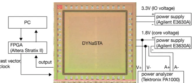
We measured the power consumptions of the fabricated chip during the con-figuration and the running phases of the DYNaSTA with fibonacci. The experi-mental setup is shown in Figure 14 and Figure 15. We implemented Mico32 on the FPGA (field-programmable gate array) and sent the test vector and clock to the fabricated DYNaSTA chip. Since DYNaSTA require 3.3 V power supply for I/O and 1.8 V for core, we supplied each power to DYNaSTA using two power supply units. Then, we connected the power analyzer to the core power supply and measured the power consumption during running. Figure 16 shows the measured power consumption versus clock frequencies for both the configura-tion and the running phases. Because of the limitaconfigura-tion of our FPGA-based pow-er-measurement workbench, the maximum frequency for the measurement was 80 MHz. We then predicted the power consumption at 100 MHz by linear in-terpolation of the measured data.
Table 3 shows a comparison of the simulated and measured (and
I. Hida et al.
[image:12.595.212.533.465.702.2]Figure 14. Experimental configuration.
Figure 15. Photograph of our power-measurement workbench.
Table 3. Comparison between simulation results and measurement results at 100 MHz.
Configuration [mW] Run [mW]
Simulation 4.03 8.57
Measurement
[image:13.595.207.539.182.292.2](interpolated) 6.63 11.20
Table 4. Mico32 vs. DYNaSTA: gate counts and average toggle rates (fibonacci).
Gate count [k gates] Average toggle rate [%]
DYNaSTA
DYN 43.6 20.0
STA 322.9 1.8
Others 80.2 9.1
All 446.8 4.9
Mico32 24.1 76.8
Ratio (DYNaSTA/Mico32) 18.48 0.06
Figure 17. DYNaSTA SoC concept toward “Dark Sillicon” era.
4. Conclusion
[image:13.595.279.467.327.534.2]I. Hida et al.
experiment, we obtained the results that power consumption reduced from 69% to 86% and energy efficiency improved from 4.5 times to 13 times. Therefore, the proposed DYNaSTA accelerator was proved to be a reconfigurable accelera-tor combining flexibility and high-energy efficiency.
Filling a chip with simple, regular, and energy-efficient array like DYNaSTA can become an interesting solution in the “Dark Silicon” [9] era (Figure 17). Here, existing domain-oriented low-power-circuit techniques such as DVFS and power gating can augment the architecture quite nicely. For instance, since only a few active stages propagate like a “wave” on the array, remaining numerous “silent” stages can be powered-off systematically to minimize the leak current
(Figure 17). Our next challenges include enhancing DYNaSTA with such low-
power-circuit techniques as well as establishing code mapping SW.
References
[1] Hameed, R., Qadeer, W., Wachs, M., Azizi, O., Solomatnikov, A., Lee, B.C., Rich-ardson, S., Kozyrakis, C. and Horowitz, M. (2010) Understanding Sources of Ineffi-ciency in General-purpose Chips. ISCA’10 Proceedings of the 37th Annual Interna-tional Symposium on Computer Architecture, Saint-Malo, 19-23 June 2010, 37-47. [2] Swanson, S. and Tayelor, M.B. (2011) Greendroid: Exploring the Next Evolution in
Smartphone Application Processors. IEEE Communications Magazine, 49, 112-119.
https://doi.org/10.1109/MCOM.2011.5741155
[3] Veredas, F.J., Scheppler, M., Moffat, W. and Mei, B. (2005) Custom Implementation of the Coarse-Grained Reconfigurable ADRES Architecture for Multimedia Pur-poses. Proceedings of the 2005 International Conference on Field Programmable Logic and Applications (FPL), Tampere, 24-26 August 2005, 106-111.
https://doi.org/10.1109/FPL.2005.1515707
[4] Ozaki, N., Yasuda, Y., Saito, Y., Ikebuchi, D., Kimura, M., Amano, H., Nakamura, H., Usami, K., Namiki, M. and Kondo M. (2011) Cool Mega-Arrays: Ultralow- Power Reconfigurable Accelerator Chips. IEEE Micro, 31, 6-18.
https://doi.org/10.1109/MM.2011.94
[5] Saito, Y., Sano, T., Kato, M., Tunbunheng, V., Yasuda, Y., Kimura, M. and Amano, H. (2010) MuCCRA-3: A Low Power Dynamically Reconfigurable Processor Array.
Proceedings of the 2010 15th Asia and South Pacific Design Automation Confe-rence (ASP-DAC), 18-21 January 2010, Taipei, 377-378.
https://doi.org/10.1109/ASPDAC.2010.5419853
[6] Motomura, M. (2002) A Dynamically Reconfigurable Processor Architecture. Mi-croprocessor Forum, October 2002.
[7] Hirao, T., Kim, D., Hida, I., Asai, T. and Motomura, M. (2013) A Restricted Dy-namically Reconfigurable Architecture for Low Power Processors. Proceedings of the 2013 International Conference on Reconfigurable Computing and FPGAs ( Re-ConFig), 9-11 December 2013, Cancun, 1-7.
[8] LatticeMico32 Open, Free 32-Bit Soft Processor.
http://www.latticesemi.com/en/Products/DesignSoftwareAndIP/IntellectualPropert y/IPCore/IPCores02/LatticeMico32.aspx
[9] Esmaeilzadeh, E., Blem, E., Amant, R.S.T., Sankaralingam, K. and Burger, D. (2012) Dark Silicon and the End of Multicore Scaling. IEEE Micro, 32, 122-134.
Submit or recommend next manuscript to SCIRP and we will provide best service for you:
Accepting pre-submission inquiries through Email, Facebook, LinkedIn, Twitter, etc. A wide selection of journals (inclusive of 9 subjects, more than 200 journals)
Providing 24-hour high-quality service User-friendly online submission system Fair and swift peer-review system
Efficient typesetting and proofreading procedure
Display of the result of downloads and visits, as well as the number of cited articles Maximum dissemination of your research work
Submit your manuscript at: http://papersubmission.scirp.org/
![Figure 1. Example of EMP power consumption breakdown [1]](https://thumb-us.123doks.com/thumbv2/123dok_us/7760625.712534/2.595.261.489.578.713/figure-example-emp-power-consumption-breakdown.webp)