Elements for Silicon Photonics
Thesis by
Matthew Borselli
In Partial Fulfillment of the Requirements
for the Degree of
Doctor of Philosophy
California Institute of Technology
Pasadena, California
2006
c
2006
Matthew Borselli
To my wife,
Acknowledgements
I would first like to thank my advisor, Oskar Painter. Oskar’s contagious passion
for science gave my research a steady momentum during my entire graduate career.
He was nothing short of exuberant over our research successes while giving me
op-timism and fortitude during extended times of disappointment. He also supported
my desire to balance our difficult workload with a life outside of Caltech. He was
always respectful of my personal time and showed great concern whenever I would
push myself too hard. Although difficult at times, Oskar’s hands-on leadership style
gave me one of the most educational experiences of my life. I can say with some
assurance that virtually every single day of my graduate career was well spent in
Oskar’s group. I feel privileged to have been one of his first students because of the
close friendship that we have formed over the years. Starting our group from empty
rooms, each day I tried to pick up as many skills from him as I could, for one very
good reason: Whether it is theory or experiment, Oskar always “gets it to work.” I
cannot explain how humbling and yet inspiring this quality is. I will not soon forget
the many things that I have learned while working with Oskar, and I hope always to
have the opportunity to learn from him.
I would also like to thank Mark Gyure for helping me get into graduate school
and for his steadfast guidance over the years. With his help, I was able to secure
two graduate fellowships from NPSC and the Moore Foundation. I thank both
insti-tutions for giving me the freedom to pursue my academic dreams without financial
worry. At Caltech, there were several classes that shaped the rest of my graduate
re-search. Inside and outside of my research, I have used the intuition that Rob Phillips
imparts on his students countless times. Kerry Vahala and Amnon Yariv also formed
Axel Scherer provided us with essential materials and processing capabilities, and Eli
Yablonovitch gave us unwavering encouragement and insightful advice on the
com-plex nature of silicon surfaces. I also thank Joe Shmulovich and Inplane Photonics
for providing us with remarkable erbium-doped glass for our microlaser devices.
I am forever indebted to Kartik Srinivasan for his tremendous help over the years.
Kartik is undoubtedly one of the smartest people I have every met, and his genius is
only outdone by his modesty. A person doesn’t have to know Kartik for very long
before they realize that Kartik’s “I’m not sure” is worth more than most everyone
else’s “it’s definitely...”. I will forever try to emulate Kartik’s unique combination of
intelligence, modesty, and happy demeanor. My happiest memories in graduate school
were hysterically laughing with Kartik over anything...good or bad. I also had the
pleasure of working closely in class and research with colleague Paul Barclay. I have
great respect for Paul’s capacity to understand any subject inside and out. Paul brings
an intense clarity of thinking and courage to any research project. Tom Johnson has
been my officemate, colleague, and friend throughout our graduate careers. I cannot
say how much I have valued sitting next to this brilliant man. The sum total of
knowledge in his head is astonishing. Whether it be swagelok fittings or the religious
symbology on the backs of automobiles, I doubt there is a conversational topic that
Tom wouldn’t be able to contribute meaningfully to. I greatly enjoyed the many
inspiring conversations that Kartik, Paul, Tom, and I had while we worked as a team
to help build Oskar’s group. I constantly strive to be a better person after being
humbled by all of their great minds. I would not be earning a PhD without them.
This thesis work could not have been completed without the help from many
other Caltech graduate students and staff. I would like to thank: Sean Spillane for
his significant help in getting started with finite-element simulations; David Henry
for his help on surface passivation techniques; Chris Michael for working out the
engineering for the dimpled fiber taper probe; Hermes Huang for his help in the
cleanroom; Colin Chrystal for figuring out how to reliably make a fiber taper; David
Gleason and Patrick Hurley for useful discussions on silicon surface chemistry; Deniz
processing advice; and Joe Haggerty at the aero shop for help in designing the many
necessary machined parts. I would also like to thank the many people who gave
me so much indirect help during my graduate career, even if it was just someone to
talk to: Raviv Perahia, Orion Crisafulli, Jessie Rosenberg, Matt Eichenfield, Stefan
Maier, Andrea Martin, Tobias Kippenberg, Brett Maune, Jeff Fingler, Martin
Smith-Martinez, Robb Walters, and everyone else I’m sure I’ve forgotten. Thank you all.
As a child, I spent nearly every other weekend helping my father work around the
house. Together, my Dad and I built block walls, garages, culverts, bicycles, and
so much more. My dad taught me how to solve problems, use tools, work as part
of a team, and have fun the entire time. Although I didn’t know it at the time,
my Dad made many sacrifices in his life so that he could have time for his kids. I
never imagined how valuable those experiences could be until I began helping to build
Oskar’s research lab. Rarely a day would go by in the lab when I wouldn’t mention
some pearl of wisdom from my dad. I cherish every minute that my dad and I spent
working together, and I cannot wait to start helping him around the house again.
Just as my father gave me the skills necessary to succeed in life, my mother gave me
the capacity to believe in myself. My mom’s infinite love for her kids inspires me to
be a better person to this day. There was nothing that my mom would not do to help
me, and there is no possible way I could ever repay her. My mother has always been,
and will continue to be, my biggest fan. I hope she knows that I am hers as well.
I also have to thank my wonderful family. I thank them for putting up with the
know-it-all child that I was, and I thank them for putting up with my idealist rants of
today. I dearly miss seeing my family as often as I used to because being with them
fills me with such joy. I am rarely as happy as when I am able to attend one of our
many family gatherings. To my friends back home and my friends with me now, thank
you for keeping me sane. I apologize for the many nights that I spent too much time
consumed by numbers and equations, when I should have been more fully enjoying my
time with you. I appreciate all that you have done for me, from planning our vacations
to protecting my sense of humor from atrophy. A special thanks goes out to all those
family and friends that are planning to attend my graduation commencement. You
To Amy, my wonderful wife. It would take me another thesis to express how I
feel about you. You have done more for me and this thesis than any other. For the
past six weeks, you have given me the food by which I have survived, the strength to
persevere, and the love that held me together. Thank you for proofreading through
200+ pages of boring physics just to make me feel better. Thank you for putting up
with my stress, and thank you for doing your best to reduce it. I respect and revere
your intelligence, patience, and devotion more than ever. It was your beautiful smile
and contagious laugh that continuously reminded me that happiness is the true goal
List of Publications
[1] P. E. Barclay, K. Srinivasan, M. Borselli, and O. Painter, “Experimental
demon-stration of evanescent coupling from optical fiber tapers to photonic crystal
waveguides,” IEE Elec. Lett. 39(11), 842–844 (2003).
[2] P. E. Barclay, K. Srinivasan, M. Borselli, and O. Painter, “Efficient input and
output optical fiber coupling to a photonic crystal waveguide,” Opt. Lett. 29(7),
697–699 (2004).
[3] P. E. Barclay, K. Srinivasan, M. Borselli, and O. Painter, “Probing the dispersive
and spatial properties of planar photonic crystal waveguide modes via highly
efficient coupling from optical fiber tapers,” Appl. Phys. Lett. 85(1) (2004).
[4] K. Srinivasan, P. E. Barclay, M. Borselli, and O. Painter, “Optical-fiber-based
measurement of an ultrasmall volume, high-Q photonic crystal microcavity,” Phys. Rev. B 70, 081306(R) (2004).
[5] M. Borselli, K. Srinivasan, P. E. Barclay, and O. Painter, “Rayleigh scattering,
mode coupling, and optical loss in silicon microdisks,” Appl. Phys. Lett. 85(17),
3693–3695 (2004).
[6] M. Borselli, T. J. Johnson, and O. Painter, “Beyond the Rayleigh scattering
limit in high-Qsilicon microdisks: theory and experiment,” Opt. Express13(5), 1515–1530 (2005).
[7] K. Srinivasan, M. Borselli, T. J. Johnson, P. E. Barclay, O. Painter, A. Stintz,
and S. Krishna, “Optical loss and lasing characteristics of high-quality-factor
AlGaAs microdisk resonators with embedded quantum dots,” Appl. Phys. Lett.
probe for photonic crystal microcavities,” IEEE Journal on Selected Areas in
Communications 23(7), 132–139 (2005).
[9] K. Srinivasan, M. Borselli, O. Painter, A. Stintz, and S. Krishna, “Cavity Q, mode volume, and lasing threshold in small diameter AlGaAs microdisks with
embedded quantum dots,” Opt. Express 14(3), 1094–1105 (2006).
[10] T. J. Johnson, M. Borselli, and O. Painter, “Self-induced optical modulation of
the transmission through a high-Q silicon microdisk resonator,” Opt. Express
14(2), 817–831 (2006).
[11] M. Borselli, T. J. Johnson, and O. Painter, “Measuring the role of surface
chem-istry in silicon microphotonics,” Appl. Phys. Lett. 88, 131114 (2006).
[12] M. Borselli, T. J. Johnson, and O. Painter, “Accurately measuring absorption
Abstract
Although the concept of constructing active optical waveguides in crystalline silicon
has existed for over twenty years, it is only in the past few years that silicon photonics
has been given serious attention as a displacing technology. Fueled by the predicted
saturation of “Moore’s Law” within the next decade, universities and industries from
all over the world are exploring the possibilities of creating truly integrated silicon
opto-electronic devices in a cost effective manner. Some of the most promising silicon
photonics technologies are chip-to-chip and intra-chip optical interconnects. Now that
compact high-speed modulators in silicon have been achieved, the limiting factor in
the widespread adoption of optical interconnects is the lack of practical on-chip optical
sources. These sources are critical for the generation of the many wavelengths of light
necessary for high-speed communication between the logical elements between and
within microprocessors. Unfortunately, crystalline silicon is widely known as a poor
emitter because of its indirect bandgap.
This thesis focuses on the many challenges in generating silicon-based laser sources.
As most CMOS compatible gain materials possess at most 1 dB/cm of gain, much
of our work has been devoted to minimizing the optical losses in silicon optical
mi-croresonators. Silicon microdisk resonators fabricated from silicon-on-insulator wafers
were employed to study and minimize the different sources of scattering and
absorp-tion present in high-index contrast Si microcavities. These microdisks supported
whispering-gallery modes with quality factors as high as 5×10⁶, close to the bulk
limit of lightly doped silicon wafers. An external silica fiber taper probe was
devel-oped to test the microcavities in a rapid wafer-scale manner. Analytic theory and
numerical simulation aided in the optimization of the cavity design and interpretation
and planar microrings. Single-mode laser oscillation was observed and carefully
char-acterized for heavily oxidized silicon microdisks. Dropped power thresholds of 690
nW, corresponding to 170 nW of absorbed power, were measured from gain-spectra
and Light in–Light out curves. In addition, quantum efficiencies for these lasers were
as high as 24%, indicating that this technology may be ready for further development
Contents
Acknowledgements iv
List of Publications viii
Abstract x
Glossary of Acronyms xxviii
Preface 1
1 Introduction 2
1.1 Thesis Organization . . . 6
2 Microdisk Optical Resonances 7 2.1 Introduction . . . 7
2.1.1 Quality Factor, Photon Lifetime, and Loss . . . 8
2.1.2 FSR and Group Velocity . . . 9
2.1.3 Finesse . . . 10
2.1.4 Mode Volume . . . 11
2.1.5 Overlap Factors . . . 11
2.2 Master Equation for Systems with Azimuthal Symmetry . . . 12
2.3 Analytic Approximation for the Modes of a Microdisk . . . 14
2.4 Finite-Element Simulations . . . 20
3 Fabrication of Silicon Microdisks 29 3.1 Introduction . . . 29
3.4 Lithography . . . 33
3.5 Etching and Cleaning . . . 37
3.6 Conclusion . . . 42
4 Optical Coupling via Fiber Taper Probes 45 4.1 Introduction . . . 45
4.2 Optical Properties of Silica Fiber Tapers . . . 46
4.3 Fabrication of Fiber Taper Probes . . . 49
4.4 Test Setup . . . 52
4.5 Modal Coupling . . . 58
4.5.1 Optical Coupling to Doublet Modes . . . 58
4.5.2 Efficient Taper-Disk Coupling . . . 62
5 Optical Loss in Silicon Microdisks 69 5.1 Introduction . . . 69
5.2 Surface Scattering . . . 71
5.2.1 Derivation of Qss from the Volume Current Method . . . 71
5.2.2 Derivation of Qβ . . . 74
5.2.3 Experiments . . . 75
5.3 Beyond the Rayleigh Scattering Limit . . . 82
5.3.1 Derivation of Qsa . . . 82
5.3.2 Experimental Results and Analysis . . . 83
5.3.3 Conclusion . . . 92
5.4 Measuring the Role of Surface Chemistry in Silicon Microphotonics . 94 5.4.1 Design of Surface–Sensitive Optical Modes . . . 95
5.4.2 Fabrication and Measurement Technique . . . 98
5.4.3 Results and Discussion of Chemical Surface Treatments . . . . 102
5.4.4 Conclusion . . . 110
5.5 Accurately Measuring Absorption in Semiconductor Microresonators . 111 5.6 Surface Encapsulation Layers . . . 117
5.6.2 Thermal Oxide Cap . . . 120
5.6.3 Conclusion . . . 123
6 Silicon-Based Lasers 124 6.1 Introduction . . . 124
6.2 Raman Effect . . . 125
6.3 Erbium-Doped Cladding Lasers . . . 130
6.3.1 Introduction . . . 130
6.3.2 Achieving Inversion in a “Two-State” System . . . 131
6.3.3 Rate Equations . . . 132
6.3.4 Cavity Design . . . 138
6.3.5 Fabrication and Test Setup . . . 144
6.3.6 Saturable Pump Absorption Measurements . . . 153
6.3.7 Identification of Optimum Pump Mode . . . 158
6.3.8 Swept Piezo Scans . . . 163
6.3.9 Stepped Piezo OSA Scans . . . 176
6.4 Outlook . . . 181
A Time-Dependent Perturbation Theory 183
B Approximate u¯s for the TM case 185
List of Figures
2.1 The south face of St. Paul’s Cathedral in London . . . 7
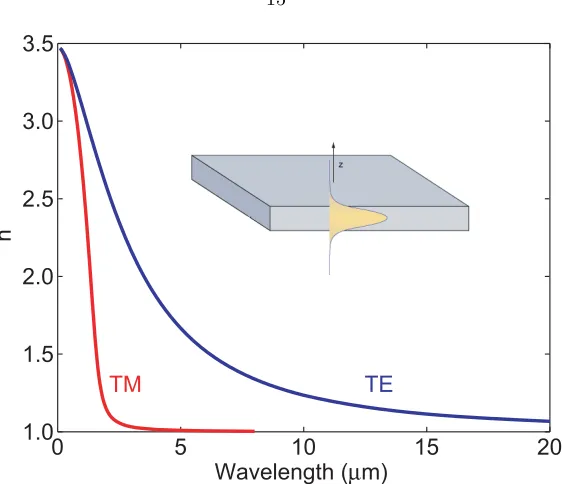
2.2 Effective slab index, ¯n, for a 215 nm thick Si microdisk. The TE slab index (blue curve) extends farther to long wavelengths versus the TM
slab index (red curve) because the TE mode is the fundamental mode
and possesses no cut-off frequency. . . 15
2.3 Analytic dispersion diagram for a 5μm radius, 215 nm thick Si microdisk against angular momentum. Shown in black are light lines at the disk
edge for air and bulk silicon. Thick blue and red lines are light lines at
the disk edge using the effective slab indices of refraction. Frequencies
outside the testable range (1400−1600 nm) have been made slightly
transparent. . . 17
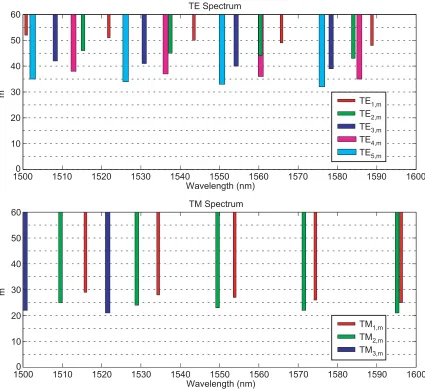
2.4 Analytic mode spectra for a 5μm radius, 215 nm thick Si microdisk for the 1500 nm wavelength band. Bars have been drawn from an arbitrary
maximum m number and drop down to mimic the mode’s predicted
coupling characteristics in a transmission spectrum . . . 19
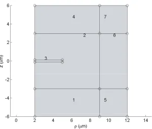
2.5 Geometry plot from Femlab 3.1 for a 5 μm radius, 250 nm thick Si microdisk. . . 21
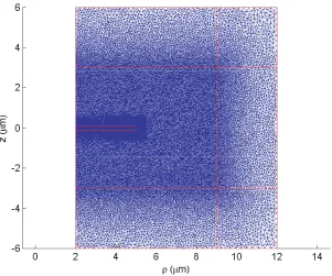
2.6 FEM mesh for a highly resolved 5μm radius, 250 nm thick Si microdisk. Mesh elements are at most 1/25 a wavelength in the material and have been refined by a factor of 2 around the disk edge periphery. Maximum
element size is 0.3 μm in PML, but nearest neighbor mesh points are specified to differ in size by <5% . . . 23 2.7 Zoomed-in view of the FEM mesh in Fig. 2.6 for a highly resolved 5μm
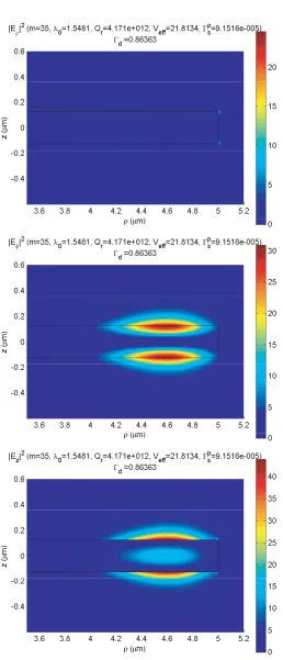
2.8 Plot of 10∗log10(|E|2) for the TM
1,35 mode atλ0 = 1548.1 nm using the
mesh shown in Fig. 2.6 for a 5 μm radius, 250 nm thick Si microdisk. . 24 2.9 Plot of Eρ, Eφ, Ez for the TM1,35 mode at λ0 = 1548.1 nm using the
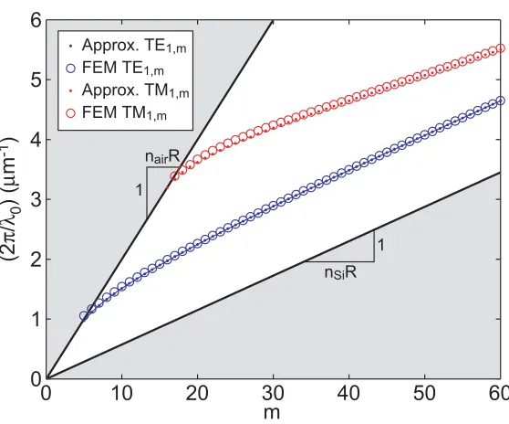
mesh shown in Fig. 2.6 for a 5 μm radius, 250 nm thick Si microdisk. . 25 2.10 Comparison of the approximate versus the FEM dispersion diagram for
a 5 μm radius, 215 nm thick Si microdisk. The blue dots and circles represent the resonance locations for the TE1,m family, solved via the
approximate and finite-element methods, respectively. Similarly, the red
dots and circles represent the resonance locations for the TM1,m family,
solved via the approximate and finite element methods, respectively. . 27
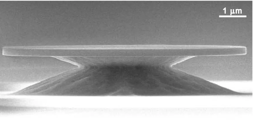
3.1 SEM micrograph of an undercut 9 μm diameter microdisk made from an SOI wafer. . . 30
3.2 Schematic illustration showing an SOI microdisk after device layer
dry-etching. . . 32
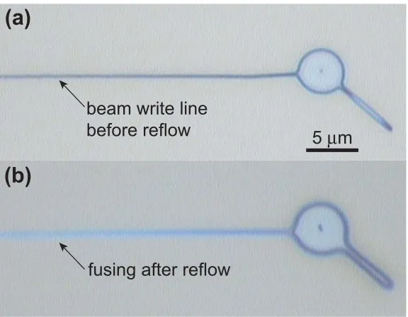
3.3 (a) 100×magnification optical microscope image of electron-beam resist
after develop. Shown is a region where electron beam rests for a short
period and then tracked to the left of the image resulting in a very
narrow gap in the ZEP resist. (b) Optical microscope image of the same
region taken at same magnification after reflowing the resist at 160◦C
for 5 minutes. . . 35
3.4 (a) 100×magnification optical microscope image of electron-beam resist
after develop and reflow at 160◦C for 5 minutes. Shown is a 10μm radius microdisk etch pattern. . . 36
3.5 SEM micrograph of a 5 μm radii microdisk after mask reflow and low bias voltage ICP/RIE etching. (a) The optimized etch using 12.0 sccm each of C4F8 and SF6. (b) An unoptimized etch using 14.5 sccm C4F8
and 12.0 sccm SF6, resulting in heavy polymerization on the sidewalls. 37
3.6 (a) SEM micrograph of a 5 μm radii microdisk after mask reflow and low bias voltage ICP/RIE etching with ZEP mask still in place. (b)
and HF undercut. . . 41
3.8 SEM micrograph of an undercut 5 μm radius microdisk. (a) Top view highlighting highly circular definition. (b) Side view of the same disk on
the same scale to show the detail of the silica pedestal. . . 43
4.1 Electric field components for the HE11 mode of a silica fiber taper with
a = 0.5 μm at λ0 = 1550 nm. The direction of propagation is assumed
to be in the y-direction, and the parity is such that the largest field component is in the vertical direction labeled as z. . . 47
4.2 Plot of the propagation constant βf of the HE11 mode versus the fiber
radius, a. The wavelength was held fixed at λ0 = 1550 nm. The index
of refraction inside the core and cladding was assumed to be 1.45 and 1.0, respectively. . . 48
4.3 Digital photographs of the custom taper pulling apparatus. Part (a)
shows the torch and fiber mounts on motorized stages. Also shown is
the arcylic enclosure used to stabilize the air currents inside the rig. (b)
Close-up view of the fiber mounts and hydrogen “hush” tip used to draw
the fiber preform gently. . . 50
4.4 Schematic drawing of the optimal placement of the fiber taper within the
hydrogen torch flame. The reaction zone of hydrogen fuel and ambient
oxygen is labeled at the “hot zone” in blue. . . 51
4.5 An approximately 1.5μm diameter fiber taper after dimpling and sub-sequent re-tensioning. . . 52
4.6 Acrylic enclosure used for testing optical devices with its front lid raised.
On the left is the micropositioning system holding the fiber taper probe,
and on the right are the x-y motorized stages that move the samples
laterally. The ultra-long working distance objective lens and zoom barrel
4.7 Optical image taken while testing a non-undercut 5μm radius microdisk with a ∼ 1.5 μm diameter dimpled fiber taper. Dimple extends down into focus from this view. . . 54
4.8 (a) Acquired “wave out” voltage from the Velocity laser versus time since
initiating the sweep through GPIB. (b) A close-up view of the software
triggering region. . . 55
4.9 (a) Acquired waveform generator voltage output used to control the
Ve-locity laser’s fine frequency piezo-stack. (b) Hysteresis curve generated
from fiber-based Mach-Zehnder interferometer. . . 56
4.10 Spectral dependence of the input power loss channels for the doublet
model with unequal standing wave linewidths assuming equal coupling
rates. Blue and green lines are the fraction of power that was transmitted
and reflected, while red and cyan dashed lines are the dissipated power
from the symmetric and anti-symmetric standing waves, Pc = γc,i|ac|2
and Ps = γs,i|as|2. Purple dashed line shows the sum of the four loss
channels, indicating power conservation. . . 61
4.11 Oscillatory dependence on the φ component of the integrand in Eq. (4.11) for a traveling wave withm = 25 coupled to a fiber with propaga-tion constant 4.8 μm−1. Shown in white is a hypothetical 5 μm radius microdisk. . . 63
4.12 Analytic dispersion diagram for a 5μm radius, 215 nm thick Si microdisk against angular momentum. Shown in black are light lines at the disk
edge for air and bulk silicon. Thick blue and red lines are light lines at
the disk edge using the effective slab indices of refraction. Frequencies
outside the testable range (1400−1600 nm) have been made slightly
nm. (a) Normalized transmission minimum as a function of taper-disk
gap with undercoupled and overcoupled regions are highlighted. (Inset)
High-magnification optical image taken with fiber taper 2μm from edge of microdisk. (b,c) Selected high-resolution transmission scans taken
from the undercoupled and overcoupled regime, as indicated by colored
astericks in (a). . . 67
5.1 SEM micrographs of a R= 2.5μm Si microdisk: (a) side-view illustrat-ing SiO2 undercut and remaining pedestal, (b) high-contrast top-view of
disk, and (c) zoomed-in view of top edge showing disk-edge roughness
and extracted contour (solid white line). . . 76
5.2 Fiber taper measurements of a TM1,44 WGM of a microdisk with R =
4.5 μm. (a) Lorentzian full-width half-maximum (FWHM) linewidth versus taper-microdisk gap. (inset) Taper transmission showing high-Q doublet. (b) Resonant transmission depth versus taper-microdisk gap.
(inset) loading versus taper-microdisk gap. . . 78
5.3 Plot of extracted contour versus arc length. . . 80
5.4 Autocorrelation function of the microdisk contour and its Gaussian fit. 80
5.5 Schematic representation of a fabricated silicon microdisk. (a) Top view
showing ideal disk (red) against disk with roughness. (b) Top view
close-up illustrating the surface roughness, Δr(s), and surface reconstruction, ζ. Also shown are statistical roughness parameters, σr and Lc, of a
typ-ical scatterer. (c) Side view of a fabricated SOI microdisk highlighting
idealized SiO2 pedestal. . . 83
5.6 Taper transmission versus wavelength showing a high-Q doublet mode for theR= 30μm disk. Qc ≡λ0/δλc andQs ≡λ0/δλs are the unloaded
quality factors for the long and short wavelength modes, respectively,
where δλc and δλs are resonance linewidths. Also shown is the doublet
5.7 Normalized doublet splitting (Qβ) versus disk radius. (inset) Taper
transmission data and fit of deeply coupled doublet demonstrating 14
dB coupling depth. . . 86
5.8 Measured intrinsic quality factor, Qi, versus disk radius and resulting
breakdown of optical losses due to surface scattering (Qss), bulk doping
and impurities (Qb), and surface absorption (Qsa). . . 88
5.9 Plot showing absorbed power versus intra-cavity energy for a R= 5 μm disk to deduce linear, quadratic, and cubic loss rates. (inset) normalized
data selected to illustrate bistability effect on resonance. . . 90
5.10 Composite of surface-sensitive thin-disk optical resonance. (a) SEM
micrograph of a 5 μm radius SOI microdisk. (b) Zoomed-in view of disk edge showing a TM polarized whispering gallery mode (WGM)
solved via the finite-element method, emphasizing large electric field in
air cladding. (c) Plot of energy density of the same WGM, emphasizing
that 78% of the energy remains in the silicon for future opto-electronic
integration . . . 96
5.11 Normalized spectral transmission response of a 5 μm radius microdisk resonator with the fiber taper placed 0.6±0.1 μm away from the disk edge and optimized for TM coupling. The spectrum was normalized to
the response of the fiber taper moved 3 μm laterally away from the disk edge. Classification of the modes is done via the notation{p, m}wherep and m are the number of antinodes radially and azimuthally, respectively. 99
5.12 (a) Normalized high-resolution scan of the TM1,31 mode at λ = 1459
nm in Fig. 5.11. Δλ and δλ indicate the CW/CCW mode splitting and individual mode linewidth, respectively. (b) Electric energy density
ter each chemical treatment and accompanying schematic of chemical
treatment. (a) Initial fabrication, illustrating surface roughness and
ab-sorption loss mechanisms. (b) Triple Piranha/HF cycle described in
Table 5.3 removes damaged material and partially passivates surfaces
states. (c) Single Piranha/HF cycle followed by an additional Piranha
allowing controlled measurement of Piranha oxide. (d) HF dip to remove
chemical oxide from previous treatment and restore passivation. . . 104
5.14 (a) Schematic representation of testing apparatus. (b) Examples of
power-dependent transmission versus wavelength data used to separate
the absorption from the total loss using the thermal bistability effect. . 112
5.15 Plot of normalized nonlinear absorption versus relative electric-field
cav-ity energy along with a linear fit. . . 113
5.16 (a) Plot of thermally-induced wavelength shift (Δλth) versus relative
dropped power (Pd) along with nonlinear and linear absorption model
fits. (inset) Global slope, Δλth/Pd, versus Pd for the same dataset. (b)
Wavelength dependent intrinsic linewidth for a family of high-QWGMs, along with the measured delineation between scattering loss and linear
absorption. Note that the fit shown in (a) was used to generate the data
point at 1447.5 nm in (b). . . 116 5.17 Summary of best linewidths after selected processing steps for 5−10
μm radii disks fabricated with a stoichiometric SiNx encapsulation layer
and forming gas anneal. . . 119
5.18 Summary of best linewidths after selected processing steps for 5−10
μm radii disks fabricated with a thermal oxide encapsulation layer along with various annealing trials. . . 121
5.19 (a) Summary of best linewidths after selected processing steps for 5−10
μm radii disks fabricated without an initial protective cap. This sample also had a thermal oxide encapsulation layer but no FGA. (b)
6.1 Schematic depiction of two-photon absorption (TPA) and the resulting
free-carrier absorption (FCA). . . 126
6.2 Broad OSA scan of reflected power from a R= 15 μm silicon microdisk showing reflected pump and stimulated Raman line. . . 128
6.3 (a) Narrow OSA scan with resolution bandwidth of 0.08 nm of Raman emission showing resonantly enhanced behavior, (b) similar narrow scan
of aR= 5μm disk illustrating decrease in density of modes as compared to (a), (inset to (b)) Raman power, PR versus input power, Pi, for the R = 5 μm disk. . . 128
6.4 Multiplet energy levels for erbium-doped oxides for the
telecommunica-tions relevant ∼ 1550 nm signal band with a ∼ 1480 nm pump. The
green dots represent Er3+ ions in a highly inverted distribution. . . 131
6.5 Assumed Er3+ spectrally varying absorption and emission cross sections,
σa(λ) and σe(λ) used throughout this work (adapted from [1, 2]). . . . 133
6.6 FEM simulations of TE polarized Er-doped cladding laser modes at
1550 nm for various buffer layer thermal oxidation times. Starting disk
parameters were: R = 20 μm radius, hSi = 195 nm, hEr = 300 nm,
tBOX = 3 μm. (a) Spatial dependence of |E(ρ, z)|2 for ΓSi= 0.28
(high-lighted by gray bar in (b)). (b) Fraction of electric energy in each
dielec-tric component versus buffer layer thickness (and equivalent remaining
silicon core). . . 139
6.7 FEM simulations of TM polarized Er-doped cladding laser modes
at 1550 nm for various buffer layer thermal oxidation times. Starting
disk parameters were: R = 20 μm radius, hSi = 195 nm, hEr = 300
nm, tBOX = 3 μm. (a) Spatial dependence of |E(ρ, z)|2 for ΓSi =
0.30(highlighted by gray bar in (b)). (b) Fraction of electric energy in each dielectric component versus buffer layer thickness (and equivalent
thickness (and equivalent remaining silicon core) for λ0 fixed at 1550
nm. Starting disk parameters were: R = 20 μm radius, hSi = 195 nm,
hEr = 300 nm, tBOX = 3 μm. . . 141
6.9 SEM micrograph of an early erbium-doped cladding silicon microdisk
after FIB cross-sectioning. Top image was taken with a 30 kV
accel-erating voltage for best resolution, while the bottom image was taken
with a 5 kV accelerating voltage for best material contrast (note: 2 nm
buffer layer is present but not discernable). . . 142
6.10 SEM images of rings after the final chemical treatments and 30 nm
thermal oxidation. (a) Top-view of a 20μm diameter, 2μm width ring. (b) Side view showing smooth ring sidewalls and a slight BOX undercut
due to the final chemical treatment. . . 145
6.11 Transmission spectrum of a high-Q mode at λ0 = 1428.7 nm on a 80
μm diameter, 2 μm width ring after final chemical treatments and 30 nm thermal oxidation. . . 147
6.12 SEM micrographs of silicon rings after chemical treatments, 30 nm
ther-mal oxidation, and 300 nm erbium-cladding deposition. (a) 20 μm ra-dius, 1 μm width ring. (b) 2 μm width ring after FIB cross-sectioning. (c) Higher magnification view of cross section where silicon core, thermal
oxide and erbium oxide are clearly visible. . . 148
6.13 Test setup used to resonantly pump the silicon microresonators and
collect the emitted light. “SP”(“LP”) refers to a short (long) pass edge
filter. The top optical image was taken with a long working distance
lens and CCD camera during testing. The dimpled fiber taper and 20
μm radius fully-oxidized microdisk with Er-doped cladding are shown. The bottom plot is an OSA power scan at the output of the two-stage
filter at maximum input power showing that only erbium emission is
6.14 Normalized transmission spectra of a 10 μm radius silicon microdisk after a 60 nm thermal oxidation and 300 nm erbium-doped glass
depo-sition. The blue scan was taken at 0.14 μW of input power, while the green scan was taken at 45 μW. The black dots indicate transmission minima for 50 intermediate powers. The red curve is a doublet fit to the
lowest power scan, and fit parameters are listed in red. . . 152
6.15 (a) Total linewidth for the resonance described in Fig. 6.14 as a function
of stored pump photons. The data was taken from a 10 μm radius silicon microdisk after a 60 nm thermal oxidation and 300 nm
erbium-doped glass deposition. (b) OSA scan of saturated emission. (Resolution
bandwidth was 0.1 nm and sensitivity was 12 pW.) . . . 155 6.16 Loss characterization for a single family of modes in a 20μm radius fully
oxidized microdisk after 300 nm of Er-doped cladding was deposited.
Blue dots represent total “cold” decay rate and red dots represent
mea-suredγpaat each wavelength for below-threshold data. (Inset) Threshold dropped powers needed to obtain lasing versus wavelength. Lasing was
always single mode at 1560.2 nm, regardless of pump wavelength. Red curve in inset is a model for expected dropped power threshold using
cross sections plotted in Fig. 6.5 and assuming γs = 1.3 Grad/s. . . 156
6.17 Broad external pump laser scan of an undercoupled fully oxidized 20
μm radius microdisk. Scan speed was 10 nm/s, and input power was 670μW. (a) Undercoupled broad-scan transmission spectrum (b) Corre-sponding photoluminescence excitation spectrum. Starred mode shows
highest external efficiency. . . 159
6.18 (a) Composite spectrum of a fully oxidized 20μm radius microdisk. 1400 nm spectrum is normalized external pump laser scan, with taper position
optimized for critical coupling to 1477.1 nm resonance. Red curve is normalized collected photoluminescence while pumping on 1477.1 nm resonance. Green dashed lines indicate the laser’s family. 1560 nm
responding photoluminescence excitation spectrum, plotted on an
ar-bitrary logarithmic scale (max peak to min peak is approximately two
orders of magnitude). Green dashed lines indicate laser’s family (seen
only in PLE). . . 162
6.20 Unidirectional photoluminescence spectrum, pumped at 1477.1 nm with 600 μW of input power. (Resolution bandwidth was 0.1 nm and video bandwidth was 60 Hz). . . 162
6.21 Swept piezo spectra of a fully oxidized 20 μm radius microdisk after 300 nm erbium-doped glass deposition. (a) Selected normalized
trans-mission spectra for 0.1 to 38 μW of input power. The black asterisks indicate transmission minima. The red curve is a doublet fit to the
lowest power scan, and fit parameters are listed in red. (b) Selected
corresponding photoluminescence excitation spectra, along with black
asterisks marking the “on-resonance” condition. . . 164
6.22 Total linewidth for the resonance described in Fig. 6.21 as a function
of stored pump photons. The data was taken on a fully oxidized 20 μm radius microdisk after 300 nm erbium-doped glass deposition. Red curve
is a saturable absorption fit using Eq. (6.17) for the below threshold data
(Mp <3000). . . 166
6.23 Pump gain (gp ≡γp−γtot,p) for the resonance described in Fig. 6.21 as a
function of stored pump photons. The data was taken on a fully oxidized
20 μm radius microdisk after 300 nm erbium-doped glass deposition. Black curve is a full rate equation fit using Eqs. (6.19a - 6.19c). . . 168
6.24 Collected signal power for the resonance described in Fig. 6.21 as a
function of stored pump photons. The data was taken on a fully oxidized
20 μm radius microdisk after 300 nm erbium-doped glass deposition. Red curve is collected lasing mode emission PL = (γext/2)(MLωL), and
green curve is collected spontaneous emission Px = (γext/2)(Mxωx)
6.25 (a) Collected signal power for the resonance described in Fig. 6.21
as a function of absorbed power, Pabs = p(Mpωp). The data was
taken on a fully oxidized 20 μm radius microdisk after 300 nm erbium-doped glass deposition. Red curve is collected lasing mode emission
PL = (γext/2)(MLωL), and green curve is collected spontaneous
emis-sion Px = (γext/2)(Mxωx) from all other modes. Black curve is total
collected powerPs =PL+Px. (b) logarithmic version of (a) to emphasize
low-power region. . . 172
6.26 (a) High-power data showing collected signal power for the resonance
de-scribed in Fig. 6.21 as a function of dropped power. The data was taken
on a fully oxidized 20 μm radius microdisk after 300 nm erbium-doped glass deposition. (Inset) Normalized transmission versus wavelength for
several input powers. (b) Zoomed-in view of the low power end of the
dataset. Red dashed curve is a linear fit to all above threshold data,
and green curve is a linear fit to above threshold data for Pd<20μW. 175
6.27 Transmission and OSA spectra used for a stepped piezo L-L curve. (a)
Blue curve is a swept piezo scan taken immediately prior to stepping the
piezo voltage (red dots) down the resonance for a fixed input power. An
∼ 1 pm drift caused by small temperature shifts between sample and external laser over the course of the stepped scan. (b) A representative
OSA spectrum for each stepped piezo voltage. The specific scan was
chosen to be near laser threshold and is marked with a star in (a). . . . 178
6.28 L-L curve for data extracted from stepped piezo scans. Blue dots
rep-resent laser mode’s photon population while green circles reprep-resent a
typical strongly coupled but nonlasing mode at 1556.3 nm. Red curve is the same fit as used in Fig. 6.24 except for a slightly modified γext
to account for slightly different taper positions. (b) Linear scale of (a)
with inset of threshold region. . . 180
B.1 Comparison of approximate form of ¯us(ˆz) and total ¯us calculated using
List of Tables
5.1 Summary of theoretical and measured mode parameters forR= 2.5 and 4.5 μm Si microdisks. Theoretical surface-scattering values for Qss and
Δλ±m are shown in parentheses. . . 77
5.2 Summary of TM1,31 characteristics after various chemical treatments . 105
Glossary of Acronyms
DEMUXDemultiplexed
BOX Buried oxide layer for SOI wafers
FCA Free-carrier absorption
FEM Finite-element method
ICP/RIE Inductively-coupled plasma / reactive ion etching
MUX Multi-plexed
OSA Optical spectrum analyzer
Q Quality factor
PECVDPlasma-enhanced chemical vapor deposition
PL Photoluminescence
PLE Photoluminescence excitation
PVDPhysical vapor deposition
SEMScanning electron microscope
SOI Silicon-on-insulator
TPATwo-photon absorption
Preface
Being a part of Oskar Painter’s group, I had many opportunities to work on one of his
passions, photonic crystals, as did both of my contemporaries, Kartik Srinivasan and
Paul Barclay. Photonic crystals represent the ultimate in control over light because of
their unique ability to lithographically control the group velocity photons experience
as a function of space. While this absolute control is necessary in some photonic
applications, the proper design and fabrication of these structures is a formidable
un-dertaking. Numerical simulations of photonic crystals require slow three-dimensional
finite difference solvers, and high quality fabrication requires extensive lithography
calibrations and etch optimizations. My brilliant friends Kartik and Paul, bravely
chose to begin their research in photonic crystals and made significant contributions
in that field, of which I played a small part. Over the years, my research gravitated
towards high-index contrast whispering-gallery modes, partly because I did not feel
optimistic in competing with Kartik and Paul and partly because my heart searched
for a path of less resistance. I believe that it is the most elegant of solutions that
produce the most utility for many reasons. An elegant solution is easily taught during
a technology’s maturity from initial idea to mass-produced widget, giving it an
ad-vantage in applied physics. As a corollary, fabrication and experiment will inevitably
become derailed many times (as mine has done time and time again!) when
attempt-ing to prototype a technology. However, by definition the elegant solution lives in
a smaller parameter space, always making it possible to rediscover the proper path
quickly. Learning to have fortitude is one of the great lessons that my advisor and
colleagues have taught me during graduate school. I would like to believe that I may
have also impressed upon them that the desire for simplicity is not always a weakness
Chapter 1
Introduction
In 1985, Richard Soref and others proposed that single-crystal silicon could be used as
an optical waveguide material [3, 4]. Inspired by silicon’s tranparency at the
telecom-munication wavelengths, 1300 and 1550 nm, they believed that silicon could be used
to add optical functionality to microelectronics applications. Their seminal papers
calculated that crystalline silicon could guide light on a chip with losses less than 0.01 dB/cm for lightly doped wafers. In addition, the guided light could also be switched
at high speeds by electronically changing the local free-carrier density. During the
next twenty years, the economies of scale present in lithographic fabrication allowed
the microelectronics industry to grow to a $160 billion dollar industry. As a
con-sequence, the vast amounts of money spent on engineering silicon as an electronic
material overshadowed Soref’s early contributions. Today the gate oxide thickness of
modern transistors is roughly five atomic layers, with eight metal wire layers required
to transport all the signals within a microprocessor. The reduced-dimension of these
metal wires amid increasing clock-speeds is beginning to cause significant cross-chip
signal latencies. To make matters worse, “Moore’s Law” scaling of transistor cost and
density is predicted to saturate in the next decade [5]. Thus, silicon-based
micropho-tonics is once again being explored for the routing and generation of high-bandwidth
signals. Optical microprocessor interconnects offer the promise of decreased
laten-cies, reduced power consumption, and immunity to electromagnetic interference. The
relatively large pitch of the top global interconnects makes the optical waveguide
an interesting alternative to exisiting copper interconnects. In May of 2004, a large
intercon-They concluded that in conjunction with wavelength division multiplexing, optical
interconnects offer a low latency alternative to existing metallic wire technologies for
global signaling.1 These optical interconnects would need to be high-index contrast
to achieve small footprints and tight waveguide turning radii. Optical losses of the
waveguides and potential on-chip laser sources would need to be kept to a minimum
for power-efficiency and heat management. Wavelength division multiplexing (WDM)
would be essential to cost effectively use all of the available bandwidth in each optical
waveguide. On-chip modulators and detectors would also be crucial for transducing
the information between optical and electronic carriers. Most importantly, the
fabri-cation processes would need to maintain CMOS compatibility in order to leverage the
near half-century of processing development in the microelectronics industry [7, 8].
At the same time, research groups around the world were making revolutionary
advances in Si optoelectronics. The first major achievement was the demonstration
of an Si optical modulator working in excess of 1 Gbit/sec [9], a 50 fold improvement
over prior art. Based on the concepts that Soref suggested 20 years prior, fast optical
modulation was achieved with free-carrier dispersion in a MOS structure. Subsequent
refinements to this technique realized modulation rates of 10 Gbit/sec [10]. Then an
all-optical high-speed switch was created [11]. Using free-carriers generated from
two-photon absorption (TPA), this work managed to switch light in less than 500
ps using light pulses with energies as low as 25 pJ. Within a year, the same group
demonstrated compact all-optical gigabit modulation with control powers of 4.5 mW [12, 13]. Photonic crystal versions using thermal bistabilities and then free-carrier
dispersion reported on similar performance with drastically reduced switching energies
[14–16]. These high-Q photonic crystal cavities were based on small perturbations to photonic crystal waveguides along with exquisite fabrication [17–22]. Around the
same time, researchers at UCLA and Intel reported the first demonstrations of a
pulsed [23, 24] and then CW silicon laser [25] based on the Raman effect.
Aiding in these and previous developments of integrated optical and electronic
Si circuits is the availability of high-index contrast silicon-on-insulator (SOI) wafers.
SOI provides the tight optical confinement of light necessary for high-density
opto-electronic integration and nonlinear optics. In addition, the high-quality underlying
thermal oxide provides simultaneous exceptional photonic and electronic isolation. As
Si microphotonic device functionality and integration advances, and light is more often
routed into the Si, it will be important to develop low-loss Si microphotonic circuits in
addition to the already low-loss glass-based planar lightwave circuits (PLCs) [26, 27].
One key element in such circuits is the microresonator. Microresonators allow light
to be distributed by wavelength or localized to enhance nonlinear interactions.
This thesis details several advances in optical design and silicon
microfabrica-tion that have allowed for the creamicrofabrica-tion of SOI-based microdisk and microring optical
resonators with extremely smooth high-index-contrast etched sidewalls [28]. These
microdisks and microrings provide tight optical confinement down to radii of 1.5μm, while maintaining the low loss of the high-purity crystalline silicon. Resonant mode
quality factors as high as Q ∼ 5×10⁶ are measured, corresponding to an effective
propagation loss as small as α ∼ 0.1 dB/cm. Inspired by the ultra-smooth glass microspheres [29, 30] and microtoroids [31] formed under surface tension, this work
uses an electron-beam resist reflow technique [32] and low DC-bias etch [33] to
signif-icantly reduce surface imperfections at a resonator’s edge. A fiber-based, wafer-scale
probing technique was also developed to rapidly and non-invasively test the optical
properties of these fabricated devices. This fiber taper probe allowed for a
compre-hensive analysis and in some cases reduction of the different optical loss mechanisms
in SOI microdisks, including the absorption of the surface-states at the edge of the
disk (for smaller microdisks) and the bulk Si free-carrier absorption due to ionized
dopants (for larger microdisks).
After carefully studying the properties of all-silicon microcavities, we sought to
create silicon optical waveguides and resonators in a hybrid material environment
capable of displacing a significant fraction of the energy from the silicon into an
en-gineered cladding while maintaining the best qualities of silicon as an opto-electronic
material. The cladding of the hybrid silicon-on-insulator (HySOI) waveguide could
be functionalized in a variety of ways for applications that benefit from large field
functional-many research groups around the world are also developing similar technology, the
methodology described in this thesis presents several technological advantages. The
basic concept is the following: in order to effectively use the engineered cladding, the
optical field of the mode must cross a silicon boundary. However, the optical
engi-neer is free to choose which silicon surface will be exposed to large field intensities.
Through chemo-mechanical polishing, the top surface of the SOI wafer can be made
to be of epitaxial quality. In contrast, the etched sidewalls of Si waveguides and
mi-crocavities will always possess significantly worse surfaces by comparison. Thus, we
optimized our mode profiles for maximum overlap with a top cladding as opposed to
a lateral cladding.
Through a combination of theory and simulation, we designed and fabricated
de-vices of predominantly TM polarization (dominant component of the electric field
polarization perpendicular to the top surface of the SOI). We found that the use
of TM modes enhanced the energy overlap with the active material around the top
silicon layer while decreasing the sensitivity to fabrication-induced imperfections in
the vertical sidewall. Upon testing, it became clear that the newly designed
mi-croresonators possessed extreme sensitivity to the top silicon surface. As a result,
surface treatments and thin encapsulation layers had to be developed in order to
preserve the quality factor upon deposition of the functionalized cladding [34, 35]. As
an initial example of the power of this technique, erbium-doped glass cladding was
deposited over the optimized structures. Through resonant optical pumping with
the fiber probe, efficient single-mode microlasers with thresholds below a microwatt
were demonstrated. In addition, resonant pumping permitted a detailed laser
perfor-mance characterization, and many key parameters were extracted from gain curves
and Light in–Light out measurements. With further engineering, these microlaser
designs will hopefully provide the first high-volume-manufacturing ready SOI optical
sources that are electrically tunable while being capable of delivering technologically
1.1
Thesis Organization
This thesis is separated into the five basic components needed to create a silicon
microlaser: microcavity theory, fabrication, optical coupling, loss minimization, and
laser realization. Chapter 2 lays the mathematical and optical physics framework
upon which this thesis is based. Beginning from some basic microcavity terminology
and the Maxwell equations, this chapter unfolds a set of results that will be useful
in understanding the later experimental observations and interpretations. Chapter 3
provides a basic but detailed fabrication recipe that is common to all of the devices
presented in this thesis. Chapter 4 not only describes the method and apparatus used
to test the microcavities, but also includes a theoretical description of how to interpret
the acquired transmission spectra. Doublet modes, evanescent coupling, and phase
matching considerations are presented in the final section of this chapter. Chapter 5
provides a more or less chronological account of our journey that was required to make
high-Q devices that were suitable for engineered claddings. Much of the later work in this chapter was done in conjunction with my colleague Thomas Johnson. The
final chapter, Chapter 6, provides a brief overview of previous work on silicon-based
lasers before taking a detailed look at Raman and erbium-doped glass lasers. The
majority of the chapter is devoted to the proper design, fabrication, and modeling
of an erbium-doped cladding laser on silicon. The appendices provide supporting
Chapter 2
Microdisk Optical Resonances
[image:35.612.252.397.296.496.2]2.1
Introduction
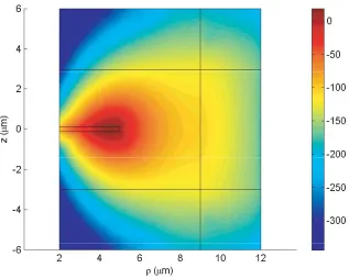
Figure 2.1: The south face of St. Paul’s Cathedral in London
In the early 20th century, a quirk of the top gallery in St. Paul’s Cathedral, shown
in Fig. 2.1, allowed whispers to be audibly heard evenly around the perimeter of
the gallery. Many top physicists including Lord Rayleigh and Raman posited
expla-nations for this effect. Subsequent testing for the next several decades showed that
Lord Rayleigh’s observations were the most telling. In describing the problem of the
whispering gallery, he wrote, “the whisper seems to creep round the gallery
horizon-tally, not necessarily along the shorter arc, but rather along that arc towards which
the whisperer faces” [36]. While these experiments were done with sound waves, the
hard walls of the gallery proves to be the same mental picture for their optical
coun-terpart. When properly excited, optical waves can be coerced to circulate around
the periphery of a circular material with high index of refraction. By optimizing
the lithographic etching, these devices can support modes that hold onto packets of
light for hundreds of thousands of round-trips before escaping to the environment.
This chapter serves as an introduction to optical microcavities, with special attention
paid to whispering-gallery modes (WGM) of silicon microdisks. After discussing the
essential microcavity terminology, the master equation for these resonances will be
outlined. Then approximate and numerically exact solutions of the master equation
will be described in great detail.
2.1.1 Quality Factor, Photon Lifetime, and Loss
Much of this thesis is concerned with maximizing the quality factor, Q, of silicon microcavities. The definition of the quality factor extends well beyond that of
mi-crophotonics and is generally defined for all resonant elements as [37, 38]
Q≡ ω·Uc Ploss
, (2.1)
where ω is the frequency of the oscillation, Uc is the stored energy in the resonator,
and Ploss is the power dissipated by the resonator. In words, Q is defined as 2π
times the ratio of the time-averaged energy stored in the cavity to the energy loss
per cycle. From conservation of power, this definition immediately implies that the
time-dependence for the decay of energy inside the resonator is given by
Uc(t) =U0e−ωt/Q, (2.2)
in the absence of further sourcing of the cavity. By a simple Fourier transform, the
quality factor can also be measured spectrally rather than by the “ring down” of the
previous equation according to
Q= ω
also measure the quality factor by wavelength according toQ=λ0/δλ, provided the
resonance is very low loss. Another common term in optical microcavity research is
the photon lifetime, τ. The photon lifetime is the time required for the energy to decay to e−1 its original value and is given by τ ≡ Q/ω. The quality factor can be related to standard absorption coefficients, α, via the group velocity of the optical energy, such that α=ω/(Qvg).1
Q is the single most important parameter to optimize for silicon microlasers be-cause the loss in a microcavity must be overcome by the gain in the microcavity. To
date, there are few high-gain materials that can be placed in the near field of a silicon
microcavity. Therefore one must create a laser through extraordinary Q’s. High-Q cavities are also important for narrowband filtering, as well as the observation of large
nonlinear and cavity QED effects.
2.1.2 FSR and Group Velocity
The free-spectral range (FSR) is defined as the frequency spacing (δωFSR) or
wave-length spacing (δλFSR) between the modes of an optical cavity. Generally speaking,
the FSR always increases as the physical size of the resonator is shrunk. The FSR
is important for both technological and scientific reasons. From a technology
stand-point, a large FSR permits the development of single-mode and high-efficiency lasers
from materials with broadband gain. A large FSR also allows for narrowband
fil-tering for dense wavelength division multiplexing (DWDM) applications without the
risk of channel cross-talk (assuming a constant Q). From a scientific perspective, the FSR provides an indirect measure of the speed of propagating packets of light inside
the resonator, otherwise known as the group velocity, vg ≡ ∂ω/∂β [37, 39]. For the
case of azimuthally symmetric resonators, the wavevector, β, changes as a function of radius within an optical mode. However, the angular wavevector, m, is always a well-defined quantity and can be used to find the linear momentum2 of the photons
in the material at any radius, ρ, according to β = m/ρ. This relation can then be
1All of the above relations are somewhat arbitrary and circular, but one should be careful to maintain a set of
self-consistent definitions.
2From this point on, I shall use the term “momentum” and “angular momentum” interchangeably with
used to relate group velocity to FSR for the case of whispering-gallery modes:
vg ≡ ∂ω ∂β =
δωFSR
m+1
ρ −
m ρ
=ρ δωFSR. (2.4)
For all but the smallest of microdisks, vg is approximately constant across the optical
mode and is given by
vg ≈R δωFSR=
2πR τrt
, (2.5)
whereτrt is an optical packet’s round-trip time. Defining the group index in terms of
the speed of light in vacuum, ng ≡ c/vg, allows connection to standard Fabry-Perot
resonators by rewriting the last equation asδνFSR =c/(2ngπR).
2.1.3 Finesse
The two previous sections have laid the ground work to describing the oftentimes
huge cavity build-up of photons inside the resonator proportional to a quantity called
the finesse, F. The finesse of a cavity is defined by [37]
F ≡ δωFSR
δω , (2.6)
and for azimuthally symmetric modes can be quickly calculated by F = Q/m. In this thesis, F can be as high as 7×10⁴, among the highest reported values of finesse
to date in semiconductor resonators. A simple argument based on the previous two
sections can put the finesse into a physically intuitive context. In steady-state, the
average number of round-trips a photon makes before leaving the cavity is given by
τ /τrt = F/(2π). Assuming a linear relationship between dropped power, Pd, and
stored cavity energy implies that the circulating power is F/(2π)Pd. Consequently,
hundreds of watts can be made to circulate inside a microcavity by dropping only
The volume an optical mode occupies is an essential but nebulous quantity to define
in microphotonics. A mode’s volume is crucial in relating the number of photons that
reside in a mode to any nonlinear effect that those photons could produce. Thus, a
common use of mode volume is in a relation such as
I = λ0 2πng
Q V
Pd, (2.7)
whereI is the optical intensity of the field inside the resonator. One way to calculate the mode volume would be to calculate the mode’s FWHM for each spatial direction
and multiply them together. A more common definition of mode volume is
V =
n2(r)|E(r)|2dV
max [n2(r)|E(r)|2]. (2.8)
By comparing the above definition to Eq. (2.7), it becomes clear that this definition of
mode volume relates dropped power to themaximum intensity inside the microcavity.
This mode volume is thus a lower bound for the volume that a mode “occupies.”
In some instances, this definition makes sense as is the case in optimally placed
quantum dots [40–42], or if one is trying to avoid nonlinearities in the cavity. However,
usually one wishes to know the spatially averaged behavior of the resonator, so a
more accurate mode volume would replace the denominator of Eq. (2.8) with an
average energy density instead of a maximum energy density. Fortunately, all of
these definitions give similar results for most cavity geometries.
2.1.5 Overlap Factors
Many physical process, including gain and loss rates, depend upon not the volume of
the optical mode, but the energy distribution throughout the mode. Whether it be
a volume or a surface, the impact that a specfic region has on the loss or gain rate
of energy for a mode depends upon the fraction of electric-energy in the region, as
Γ =
δV n
2(r)|E(r)|2
dV
n2(r)|E(r)|2dV . (2.9)
An important example of the utility of this definition is in determining the modal gain
or loss rate of a homogeneous dielectric region based on its material characteristics.
Sometimes, these regions cannot be accurately described as a volume because they
are just monolayers thick [43]. As described in Section 5.4, surface chemistries
of-tentimes simply terminate dangling bonds or allow for energetically favorable dimer
formations. In addition, high-temperature anneals of Si/SiO2 interfaces have
imper-ceptable volumetric effects but demonstrably account for large changes in optical loss
due to surface reconstructions. Thus for surface regions of interest (δA), the best modal parameter to use is
Γ =
δAn
2(r)|E(r)|2
dA
n2(r)|E(r)|2dV . (2.10)
As most surface effects occur at regions of dielectric and field discontinuity, the
arith-metic average of each side of the discontinuity is used in calculating the above surface
integral. Γ can always be related back to a volumetric energy fraction by assuming
some physical depth to the surface, ts, and writing Γ = Γts.
2.2
Master Equation for Systems with Azimuthal Symmetry
In 1865, J. C. Maxwell predicted that the light around us was an electromagnetic
phe-nomenon and that “light” of all frequencies could be produced using a symmetrized
form of the once static laws of electricity and magnetism [38]. In the absence of free
charges or currents, these equations become
∇ ·D(r, t) = 0 ∇ ×E(r, t) = −∂B(r, t) ∂t ∇ ·B(r, t) = 0 ∇ ×H(r, t) = ∂D(r, t)
∂t ,
(2.11)
where D(r, t) = (r)E(r, t) and H(r, t) = μ1
oB(r, t) are the linear constitutive
rela-tions.3 Without free charges or currents, the only solutions to Eqs. (2.11) are
to give
∇ ·D(r) = 0 ∇ ×E(r) =iωB(r) ∇ ·B(r) = 0 ∇ ×H(r) =−iωD(r),
(2.12)
where, the real physical fields are given by[E(r, t)],[B(r, t)], etc. Taking the curl of the top right equation, representing Faraday’s Law, gives the master equation for
the electric field,
∇ × ∇ ×E(r)−k02n2(r)E(r) = 0, (2.13)
where k0 = ω/c, c2 = 1/(μ00), and n2(r) = (r)/0. Equation (2.13) (or the
sim-ilar version for the magnetic field) can be viewed as the most general of eigenvalue
equations for the optical modes of a microcavity. This work will focus on a
par-ticular simplification of the master equation where the index of refraction possesses
an azimuthal symmetry so that n2(r) = n2(ρ, z), working in cylindrical coordinates.
Another useful form of Eq. (2.13) can also be derived from the Maxwell equations
according to
∇2E+∇
1
n2(ρ, z)E(r)· ∇n 2(ρ, z)
+k20n2(ρ, z)E(r) = 0, (2.14)
where the relation∇·E =−(1/)E·∇was used [38]. This form of the master equation provides additional insight into the nature of whispering-gallery modes, because the
equation directly reduces to the vector wave equation for a piecewise homogeneous
material. Whenever a curvilinear translational symmetry is assumed to the Maxwell
equations, a reduction in the equation space takes place. This is because Eq. (2.14)
can always be separated into solving for just the transverse electric fields, just the
transverse magnetic fields, or just the two longitudinal fields [44].
2.3
Analytic Approximation for the Modes of a Microdisk
At this point, it is useful to make a few rather large approximations which allow us to
arrive at approximate but analytic solutions to the still general Eq. (2.14).
Assum-ing a piecewise homogeneous medium, Eq. (2.14) can be reduced to the Helmholtz
equation
∇2F+k2 0n
2(ρ, z)F(r) = 0, (2.15)
where F = {E,H}. Explicitly writing out the Laplacian operator in cylindrical coordinates,
∂2
∂ρ2 +
1 ρ ∂ ∂ρ + 1 ρ2 ∂2
∂φ2 +
∂2
∂z2 +k 2 0n
2
(ρ, z)
F(r) = 0. (2.16)
In a semiconductor microdisk, the vertical confinement restricts the movement of
the photon to travel in a plane rather than in three dimensions, effectively reducing
the problem to a two-dimensional one. As long as the vertical thickness is not smaller
than half a wavelength in the material, the optical mode’s field distribution becomes
quite simple. In this case, there are two dominant polarizations labeled as TE (E field parallel to the disk plane) and TM (E field perpendicular to the disk plane), where Eq. (2.16) becomes scalar in the ˆz direction. As a consequence,Fz corresponds
to Hz(Ez) for TE(TM) modes. For ρ < R, where R is the disk radius, separation of
variables can be used to rewrite Eq. (2.16) as
1 W
∂2W
∂ρ2 +
1 ρ ∂W ∂ρ + 1 ρ2
∂2W
∂φ2
+ 1
Z d2Z
dz2 +k 2
on
2
(ρ, z) = 0, (2.17)
where Fz =W(ρ, φ)Z(z). Thus we have two differential equations,
∂2W ∂ρ2 +
1 ρ ∂W ∂ρ + 1 ρ2
∂2W ∂φ2
+k20n¯2(ρ)W = 0 (2.18) d2Z
dz2 +k 2 0
n2(z)−¯n2Z = 0, (2.19)
to self-consistently solve for the free-space wave vector, k0 and the effective index,
¯