Thesis by
James Franklin Buckwalter
In Partial Fulfillment of the Requirements
for the Degree of
Doctor of Philosophy
California Institute of Technology
Pasadena, California
2006
2006
James Franklin Buckwalter
All Rights Reserved
Some materials previously published in IEEE publications and copyright is owned by IEEE.
Professor Ali Hajimiri has been a great friend as well as an advisor, and I have been
fortunate to collaborate with him at Caltech. Ali has taught me much beyond research and
I appreciate the time and effort he has put into my thesis work. His dedication to his
students is inspiring, and I am proud to be a branch on the Hajimiri family tree.
I give special thanks to Dr. Behnam Analui. He was a wonderful collaborator, and I
was very lucky to share three years of my Ph.D. with him. His patience, dedication, and
intelligence helped keep me motivated, and it was always great to brainstorm with
Behnam over Koobideh. Since his graduatation, we have all missed his presence.
I would like to thank Professor David Rutledge for his guidance over the last decade!
As an undergraduate advisor, he helped me get into a laboratory and get my hands dirty
with RF electronics. He has always been there to talk: politics or research. I thank him for
his time and patience while serving on my candidacy and thesis committees.
I am indebted to Dr. Mehmet Soyuer from IBM Research for making the trip to
Caltech twice to be a part of my candidacy and thesis committee. I also thank Professor
Sander Weinreb for serving on my thesis committee as well as Professor P. P.
Vaidyanathan for help with my candidacy committee.
The members of the Caltech High-Speed Integrated Circuit Group were always patient
and willing to make suggestions and comments regarding this work. In particular, I would
like to thank Abbas Komijani, Arun Natarajan, Professor Hossein Hashemi, Ehsan
Afshari, Professor Donhee Ham, Dr. Roberto Aparicio, Dr. Xiang Guan, Dr. Chris White,
Professor Hui Wu, and Aydin Babakhani. Special thanks to Sam Mandagaran for sharing
his curiosity with me and to Michelle Chen, who kept our lab together. Additionally, much
particular, Naveed Near-Ansari, John Lilley, Linda Dosza, Veronica Robles, Heather
Jackson, Lyn Hein, and Janet Couch have all been very helpful.
I also thank Professor Robert York at the University of California at Santa Barbara.
Professor York was a great advisor and stimulated my interest in coupled oscillator arrays.
I appreciate the years I spent in Santa Barbara. Additionally, Paolo Maccarini was a
wonderful colleague and friend at Santa Barbara.
I am grateful to IBM for awarding me with an IBM Ph.D. Fellowship which included
the wonderful Thinkpad on which this thesis was written. I want to recognize the
contribution of IBM Research in Yorktown Heights, New York. In particular, Drs. Mounir
Meghelli, Alexander Rylyakov, Sergei Rylov, John Bulzachelli, Jose Tierno, Dan
Friedman, and Sudhir Gowda were great colleagues during my summer internship at IBM.
Additionally, Dr. Micheal Beakes, Troy Beukama, Dr. Mark Ritter, Dr. Mehmet Soyuer,
and Dr. Modest Oprysko all helped make my summer productive and enjoyable.
I thank IBM Research for supplying us with fabrication technology for our integrated
circuits. Additionally, Rogers Corporation contribution of Duroid is also appreciated.
To my friends, East and West coast, I thank you for your understanding and support
throughout my Ph.D: Lauren, Tara, Gabe, and Sully in New York; Bryn, Matt, and Tracy
in PA; Reni and Rik in Columbus, OH; Tim, Mark, Karl, Jesse, and Justin in Santa
Barbara; and Lisa, Ian, Molly, Noah, and Vandana in Pasadena. Special thanks to the
Kollmeier family: Mama, Alexa, Marisa, Michelle, and Brett and Vicky. I’ve been
fortunate to spend so many holidays with you.
Finally, I have been lucky to share these years with my Grandparents, Rachel and
Franklin Buckwalter, in Reading, PA, and Levi and Phyllis Arehart, in Augusta, KS.
You’ve been asking me “how much longer?” for so many years and now I have an answer.
To my parents, Brian and Marcia, who have supported me throughout graduate school. I
always had quiet place to work at home. My sister, Amy, gets special thanks for putting up
Abstract
The past decade has witnessed a drastic change in the design of high-speed serial links.
While Silicon fabrication technology has produced smaller, faster transistors, transmission
line interconnects between chips and through backplanes have not substantially improved
and have a practical bandwidth of around 3GHz. As serial link speeds increase, new
techniques must be introduced to overcome the bandwidth limitation and maintain digital
signal integrity. This thesis studies timing issues pertaining to bandwidth-limited
interconnects. Jitter is defined as the timing uncertainty at a threshold used to detect the
digital signal. Reliable digital communication requires minimizing jitter.
The analysis and modeling presented here focuses on two types of deterministic jitter.
First, dispersion of the digital signal in a bandwidth-limited channel creates
data-dependent jitter. Our analysis links data sequences to unique timing deviations
through the channel response and is shown for general linear time-invariant systems. A
Markov model is constructed to study the impact of jitter on the operation of the serial link
and provide insight in circuit performance. Second, an analysis of bounded-uncorrected
jitter resulting from crosstalk induced in parallel serial links is presented.
Timing equalization is introduced to improve the signal integrity of high-speed links.
The analysis of deterministic jitter leads to novel techniques for compensating the timing
ambiguity in the received data. Data-dependent jitter equalization is discussed at both the
receiver, where it complements the operation of clock and data recovery circuits, and as a
phase pre-emphasis technique. Crosstalk-induced, bounded-uncorrected jitter can also be
compensated. By detecting electromagnetic modes between neighboring serial links, a
transmitter or receiver anticipates the timing deviation that has occurred along the
Demands of wireless communication and the high speed of Silicon Germanium transistors
provide opportunities for unique radio architectures for submillimeter integrated circuits.
Scalable, fully-integrated phased arrays control a radiated beam pattern electronically
through tiling multiple chips. Coupled-oscillator arrays are used for the first time to
subharmonically injection-lock across a chip or between multiple chips to provide phase
Table of Contents
Acknowledgments...iii
Abstract ... vi
List of Figures ...xiii
List of Tables ... xxi
Chapter 1
Introduction
1
1.1 Background: The Evolution of Serial Communications ... 41.2 Organization ... 7
Chapter 2
Signal Integrity in Broadband Communications
10
2.1 Shannon’s Theorem... 112.1.1 Signal Power ... 11
2.1.2 Noise Power... 13
2.1.3 Bandwidth... 13
2.1.3.1 High-Speed Serial Links ... 14
2.1.3.2 Optical Links ... 16
2.1.4 Capacity ... 18
2.2 High-Speed Signal Integrity... 19
2.2.1 Bit Detection ... 19
2.2.2 Voltage and Timing Margins... 20
2.2.3 Modeling of Intersymbol Interference and Data-Dependent Jitter... 21
2.2.4 Random Noise and Jitter in Bit Error Rate ... 25
2.2.5 Jitter and Clock Recovery... 29
2.3 Definitions of Jitter ... 34
2.4 Sources of Jitter in Communication Links... 35
2.4.1 Transmitter Jitter... 38
2.4.2 Channel Jitter ... 41
2.4.3 Receiver Jitter ... 43
2.5 Summary ... 44
Chapter 3
Analysis of Data-Dependent Jitter
46
3.1 Introduction ... 463.2 Analysis of Data-Dependent Jitter ... 47
3.2.1 First-Order Response ... 48
3.2.3 Experimental Results for First- and Second-order Filters. ... 56
3.2.4 Experimental Results for Transmission Lines ... 60
3.3 Data-Dependent Jitter in 4-PAM... 62
3.4 Duty Cycle Distortion ... 64
3.5 Markov Sampling of Threshold Crossing Times ... 67
3.5.1 Time Domain: Cycle-to-Cycle Behavior ... 68
3.5.2 Frequency Domain Interpretation: Jitter Power Spectral Density ... 72
3.5.2.1 Rising and Falling Edges Sensitivity ... 73
3.5.2.2 Rising Edges Only... 74
3.5.2.3 Jitter Power Spectral Density Simulations ... 75
3.5.3 Circuit Implications: Hogge Phase Detector ... 77
3.6 Summary ... 78
Chapter 4
Equalization of Data-Dependent Jitter
80
4.1 Introduction ... 804.2 DDJ Equalization ... 81
4.2.1 Eye Improvement with DJE in a First-Order Channel ... 85
4.2.2 Comparison to Decision Feedback Equalization... 85
4.3 Circuit Implementations... 87
4.3.3 DJE and CDR (DJE CDR)... 87
4.3.4 CMOS DJE ... 90
4.4 Results ... 92
4.4.5 DJE CDR ... 94
4.4.6 CMOS DJE ... 97
4.4.7 Trade-off between DDJ Compensation and RJ. ... 100
4.5 Summary ... 102
Chapter 5
Phase Pre-emphasis Techniques
103
5.1 Introduction ... 1035.2 Analysis of One-Tap Transmit Pre-Emphasis ... 105
5.3 Power and Signal Integrity in Bandwidth-Limited Channels ... 107
5.4 Phase Pre-emphasis ... 111
5.5 Circuit Implementation ... 116
5.6 Results ... 121
5.7 Summary ... 126
Chapter 6
Crosstalk-Induced Jitter
128
6.1 Introduction ... 1286.2 Crosstalk in Transmission Lines ... 129
6.3.1 Experimental Measurements of Time of Flight ... 136
6.3.2 Effect of Timing Offset Between Victim and Aggressor... 137
6.4 Crosstalk Jitter in M-PAM ... 139
6.4.1 2-PAM... 139
6.4.2 4-PAM... 141
6.5 Summary ... 143
Chapter 7
Crosstalk-Induced Jitter Equalization
144
7.1 Introduction ... 1447.2 M-PAM Crosstalk-Induced Jitter Equalization ... 145
7.2.1 2-PAM... 145
7.2.2 4-PAM... 146
7.3 Circuit Implementation ... 147
7.4 Results ... 151
7.5 Summary ... 155
Chapter 8
Subharmonic Coupled Oscillators Arrays
156
8.1 Introduction ... 1568.2 Coupled Oscillators ... 158
8.3 Scalable 2D Oscillator Array ... 160
8.3.1 Interconnections... 160
8.3.2 Frequency Doubler ... 162
8.3.3 Oscillator Injection Locking ... 166
8.4 Results ... 167
8.5 Summary ... 174
Chapter 9
Conclusions
175
9.1 Thesis Summary... 1759.2 Future Investigation ... 178
Appendix A First-Order Threshold Crossing Times
181
A.1 Threshold Crossing Times and Mean and Variance... 181A.2 Cycle-to-nth Cycle Jitter ... 183
List of Figures
Chapter 1 Introduction
Figure 1.1 An overview of the applications for high-speed communication cir-cuits. Server photo courtesy of Caltech’s Center for Advanced Computing Research...3 Figure 1.2 A basic communication link demonstrating the transmitter and receiver functions...4
Chapter 2 Signal Integrity in Broadband Communications
Figure 2.1 A basic communication link demonstrating the transmission of a 2-PAM signal over a broadband channel and the receiver recovery of the signal...10 Figure 2.2 Power spectral density of the NRZ data sequence and white noise...12 Figure 2.3 Bandwidth for butterworth filters with different roll-offs. ...14 Figure 2.4 FR4 backplane with peripheral boards and connectors for serial
com-munication. ...15 Figure 2.5 Signal attenuation for a commercial FR4 material and for a shielded
cable. ...16 Figure 2.6 The Shannon capacity as a function of bandwidth. ...18 Figure 2.7 Digital regeneration through sampling of the analog signal in a compar-ator. ...19 Figure 2.8 Illustration of the analog signal as a data eye and signal integrity defini-tions...20 Figure 2.9 The reduction of voltage and timing margins due to ISI and DDJ in a
first-order system as a function of bandwidth. ...22 Figure 2.10 Cumulative distribution function for BER for DDJ and ISI in the
absence of random noise. The margins are the gap in the center of each bathtub. ...23 Figure 2.11 The data-dependent jitter generated over RG-58 cable at 10Gb/s and
jitter histograms. ...24 Figure 2.12 Random noise and jitter distributions and their relationship to the data
margins and timing margins are represented by gap in the center of the data eye. ...28 Figure 2.14 Two-dimensional plot of the BER. The color contours follow the trajec-tories of the signal...28 Figure 2.15 Phase-locked loop for clock and data recovery. Any jitter on the data is transferred to the recovered clock...29 Figure 2.16 Linear model of a charge-pump PLL...30 Figure 2.17 BER under the influence of sampling uncertainty. The transition edges
and sampling uncertainty are governed by different random pro-cesses. ...33 Figure 2.18 Definitions for (absolute) jitter and cycle-to-cycle jitter. ...34 Figure 2.19 Categorization of different jitter sources of total jitter ...36 Figure 2.20 A basic model for the accumulation of jitter through a communication
link. ...37 Figure 2.21 Phase-locked loop for clock multiplication. A low-phase noise crystal
oscillator is used to reduce the phase noise of a 10GHz VCO. ...38 Figure 2.22 Chain of buffers and line driver in transmitter. Each stage contributes
additional random jitter due to thermal sources in the MOS devices and resistors. ...40 Figure 2.23 Thermal noise of terminations also adds random jitter. The bandwidth
limitation of the channel impacts the variance of the additional jit-ter. ...42
Chapter 3 Analysis of Data-Dependent Jitter
Figure 3.1 The generation of the transmitted data sequence into DDJ through a bandwidth-limited channel. ...47 Figure 3.2 Normalized threshold crossing time with respect to the bit rate and sys-tem bandwidth for the first-order syssys-tem and different bit sequence lengths. ...50 Figure 3.3 Data-dependent jitter mean and conditioned mean for determining the
average probabilistic behavior. ...52 Figure 3.4 Threshold crossing time with respect to the bit rate and system
band-width for second-order system. The intersection of the dashed lines demonstrates the data-dependent jitter minimization. ...54 Figure 3.5 Hypothetical pulse response that minimizes jitter in a second-order sys-tem. ...55 Figure 3.6 Comparison of the first-order response DDJ prediction with
Figure 3.7 Data eyes for first-order response at (a) α = 0.1 and (b) α = 0.31 from Figure 3.6. ...57 Figure 3.8 Comparison of second-order prediction and measured DDJ on the left
axis and corresponding rms jitter on the right axis. ...58 Figure 3.9 Threshold crossing eye diagram with superimposed histogram at
nor-malized bit rate of (a) 2 and (b) 2.9 from Figure 3.8. ...58 Figure 3.10 Received pulse response at the point of the jitter minimization and the
measured waveform. ...59 Figure 3.11 FR-4 transmission line experimental set-up. ...60 Figure 3.12 S-parameters and step response for transmission lines constructed in
Figure 3.11. ...60 Figure 3.13 Data-dependent jitter measured in FR4 coupled transmission line. ....61 Figure 3.14 Data eye for 4-PAM signal transmission. ...62 Figure 3.15 Normalized threshold crossing time for 4-PAM with respect to system
bandwidth...64 Figure 3.16 The effect of a voltage threshold offset is to introduce additional timing ambiguity in the data eye. ...65 Figure 3.17 The state space progression for the threshold crossing times where k = 3. The fast events are highlighted in dark blue while the slow states are highlighted in light blue. ...68 Figure 3.18 The cycle-to-nth cycle and cycle-to-cycle behavior of the first-order
response with and without a voltage threshold offset. ...71 Figure 3.19 The cycle-to-nth cycle and cycle-to-cycle behavior of the first-order
response for rising edge sensitivity. ...71 Figure 3.20 Autocovariance for data transition phase in a first-order system. ...74 Figure 3.21 Jitter power spectral density for first-order response with rising and
falling edge sensitivity. ...76 Figure 3.22 Jitter spectral density for first-order response with rising edge
sensitiv-ity. ...76 Figure 3.23 Modifications to a Hogge phase detector to rejection jitter. The original phase detector is sensitive to rising and falling edges. The modified circuit is only sensitive to rising edges. ...77
Chapter 4 Equalization of Data-Dependent Jitter
Figure 4.1 Definition for tails of pulse response for DDJ equalization. ...82 Figure 4.2 The block diagram for the DJE and the extension, shown in gray, for
Figure 4.4 Opening a closed data eye with the use of only DDJ compensation. ..85
Figure 4.5 Theoretical timing and voltage margin improvement for first-order channel with DJE. ...86
Figure 4.6 Chip microphotograph of the DJE CDR.The circuit includes an on-chip loop filter...88
Figure 4.7 The circuit diagram for the DJE CDR. ...89
Figure 4.8 Chip microphotograph of the CMOS DJE...90
Figure 4.9 Schematic for the CMOS DJE. Inset includes schematic for low-power CML AND gate and delay cell. ...91
Figure 4.10 Testing schemes for generating DDJ. ...92
Figure 4.11 Eyes with variable amounts of DDJ for testing. ...93
Figure 4.12 Phase noise of the recovered clock under various test conditions. ...94
Figure 4.13 Typical eye and recovered clock from the DJE CDR with no DDJ...95
Figure 4.14 Timing jitter of the recovered data (top) and the recovered clock (bot-tom) for the DJE CDR. ...96
Figure 4.15 Bathtub curve of sampling time and sampling voltage before and after equalization for DJE CDR. ...96
Figure 4.16 Data eyes demonstrating compensation of different edges and the jitter statistics associated with each edge. ...98
Figure 4.17 Bathtub curve before and after equalization in CMOS DJE...100
Chapter 5 Phase Pre-emphasis Techniques Figure 5.1 Block diagram for pre-emphasis driver. ...105
Figure 5.2 Pulse response curves for different pre-emphasis gains (fc=0.1fb). ..109
Figure 5.3 Variation of signal integrity with pre-emphasis gain. ...110
Figure 5.4 Constrained power contour for channel with first-order response (fc=0.2fb). ... 111
Figure 5.5 Data eye showning the contribution to data-dependent jitter of previous transitions...112
Figure 5.6 Phase pre-emphasis operation and truth table...113
Figure 5.7 Operation of phase and amplitude pre-emphasis. ...114
Figure 5.8 Power consumption as a function of bit rate for various channel cutoff frequencies with and without the use of phase pre-emphasis. ...115
transmits the current data bit, while the pre-emphasis multiplexer, in gray, is cross-coupled to transmit an inverted replica of the previ-ous data bit. ...117 Figure 5.11 Phase pre-emphasis implementation. The logical gates calculate the
existence of transitions in the data sequence for the past four bits. The multiplexers adjust the clock phase. ...118 Figure 5.12 Delay introduction and clock duty cycle operation. Four clock phases
are individually adjusted for the DDJ compensation and then ANDed to create the appropriate duty cycle...119 Figure 5.13 Delay generation schematic. Detailed schematics are presented for the
delay cell, clock amplifier, and DCD compensation circuits...120 Figure 5.14 Chip microphotograph of two breakout sites. Top site does not have
phase pre-emphasis. Bottom site features phase pre-emphasis. ..121 Figure 5.15 Data eyes at 6Gb/s and 10Gb/s demonstrating amplitude and phase
pre-emphasis. The first row shows the amplitude pre-emphasis at 6Gb/s as a function of pre-emphasis current. The second row illus-trates the phase pre-emphasis as a function of the compensation code. Finally, the last row shows the operation of the transmitter at 10Gb/s. ...122 Figure 5.16 Total and data-dependent jitter versus phase pre-emphasis codes for the first previous transition. The variation in DDJ can be used to calcu-late the time delay variation...123 Figure 5.17 Performance on 96” of RG-58 cable. The uncompensated eye is shown in a) while phase pre-emphasis is introduced in b) and c)...124 Figure 5.18 Performance on 16” of FR-4 backplane with connectors. The
uncom-pensated eye is closed in a). In b), amplitude pre-emphasis opens the eye and phase pre-emphasis improves the DDJ in c). ...125 Figure 5.19 Power consumption per bit rate as a function of bias current...126
Chapter 6 Crosstalk-Induced Jitter
Figure 6.1 The crosstalk jitter generated in the data eye due to the influence of a neighboring signal...128 Figure 6.2 Lossless coupled transmission line model consisting of the self
capaci-tance and induccapaci-tance and mutual capacicapaci-tance and induccapaci-tance. ...130 Figure 6.3 Electromagnetic modes that occur between the coupled transmission
line during binary digital communication...130 Figure 6.4 Comparison of calculated and measured inductances and capacitances
predicted mutual inductance and capacitance are compared to an
ADS transient simulation...137
Figure 6.6 Timing offset between the aggressor and victim data at 5Gb/s does not dramatically affect the rms and peak-to-peak jitter...138
Figure 6.7 2-PAM data eyes at 10Gb/s shown with and without the aggressor. .140 Figure 6.8 4-PAM data eyes at 10Gb/s shown with and without the aggressor. .143 Chapter 7 Crosstalk-Induced Jitter Equalization Figure 7.1 Schematic of a two-channel crosstalk-induced jitter equalization. The circuit detects the difference in the data on adjacent channels to determine the electromagnetic mode. ...145
Figure 7.2 Schematic of a two-channel 4PAM crosstalk-induced jitter equaliza-tion. ...146
Figure 7.3 Chip microphotograph of the crosstalk-induced jitter equalizer...147
Figure 7.4 Implemented version of two-channel CIJ equalizer. ...148
Figure 7.5 Schematic and operation of the mode multiplexer...149
Figure 7.6 Schematic of the delay cell. The sizing of the two differential pairs con-trols the relative delay variation that can be achieved. ...150
Figure 7.7 Transient and analytic delay variation. ...151
Figure 7.8 Data eyes at 10Gb/s before and after equalization. ...152
Figure 7.9 Data eyes at 5Gb/s before and after equalization. ...153
Figure 7.10 Bathtub curve resulting before and after equalization at 10Gb/s...154
Figure 7.11 Bathtub curve resulting before and after equalization at 5Gb/s...155
Chapter 8 Subharmonic Coupled Oscillators Arrays Figure 8.1 Coupled oscillator approach for fully integrated phased-array transmit-ter. Each oscillator drives a transmit chain with a DAC controlled phase shifter, power amplifier, and antenna...157
Figure 8.2 Unilateral injection scheme and relationship between frequency and phase detuning. ...158
Figure 8.3 Implemented coupled oscillator topology. The oscillators are coupled along two dimensions. The coupling network operates at one-third the carrier frequency. ...160
Figure 8.4 Interconnect structure with severed bathtub to prevent coupling to inte-grated antenna. ...161
Figure 8.5 Measured interconnect S-parameters over 1mm of interconnect. ...162
Figure 8.7 Current injected at oscillator frequency and subharmonic. ...165 Figure 8.8 S-parameters for coupled transmission lines in VCO...166 Figure 8.9 Chip microphotograph for complete 60GHz transmitter with coupled
oscillator array...168 Figure 8.10 Tuning range for each oscillator in 2x2 array. The difference between
the natural frequencies of each oscillator is greatest near the bottom of the tuning range. ...168 Figure 8.11 Phase noise of reference, injection locked oscillator, and unlocked
oscillator...169 Figure 8.12 Locking range for the VCO as a function of injected power. ...170 Figure 8.13 Phase noise of each oscillator in 2x2 single chip array without (Top)
and with (Bottom) injection locking. ...171 Figure 8.14 Phase of each oscillator in array across locking range. ...172 Figure 8.15 Phase noise of NW oscillator as a function of frequency detuning. ..172 Figure 8.16 Phase noise of oscillators across a 1x4 array with 2 chips. ...173 Figure 8.17 Oscilloscope waveforms for 20GHz injection across 1X4 array. ...173
Chapter 9 Conclusions
List of Tables
Chapter 2 Signal Integrity in Broadband Communications
Table 2.1: Recently Recorded Transmitter Jitter in SONET Transceivers...40
Chapter 3 Analysis of Data-Dependent Jitter Table 3.1: Calculated and Measured DDJ for FR4 Coupled Microstrip ...61
Chapter 4 Equalization of Data-Dependent Jitter Table 4.1: DDJ generated from coupled wires scheme (Vsignal = 750mV) and an-ticipated CDR jitter. ...93
Table 4.2: DDJ introduced in the load amplifiers of CMOS DJE. ...97
Table 4.3: DDJ improvement at 10Gb/s (ps) for CMOS DJE. ...97
Table 4.4: Data-dependent jitter contribution at 10Gb/s for CMOS DJE...99
Chapter 6 Crosstalk-Induced Jitter Table 6.1: Crosstalk-Induced Jitter in 2-PAM. ...141
Table 6.2: Crosstalk-Induced Jitter in 4-PAM. ...142
Chapter 7 Crosstalk-Induced Jitter Equalization Table 7.1: Improvement of Crosstalk-Induced Jitter at 5 and 10Gb/s. ...154
Appendix A First-Order Threshold Crossing Times Table A.1: List of Threshold Crossing Times in a First-order Response, k = 4. .181 Table A.2: Possible Transitions for Cycle-to-nth Cycle Jitter (Rising and Falling Edges) ...184 Table A.3: Possible Transitions for Cycle-to-nth Cycle Jitter (Rising Edge Only)...
Chapter
1
Introduction
The rapid expansion of communication technologies is profoundly impacting our
society. In the past hundred years, information exchange, once limited to letters and
telegraphs, moves near the speed of light and is accessible to the general public. With
estimates of the number of households in the United States subscribing to cable and
direct-subscriber lines (DSL) data services topping 25 million in 2005, broadband access
is indispensable [1]. Our society, once satisfied with telephony, creates more information
and services to take advantage of the growing information capacity. This trend drives the
demand for data communication, which has superseded the original role of telephony
networks for voice communication. Business and consumer demands encourage future
investment in communication technologies. Integrated circuit technologies for high-speed
communication are central to the development of new networks.
Since the development of Arpanet, the first computer network for military applications
in the 1960s, high-speed data communication technologies have proliferated throughout
society. Several factors have contributed to this proliferation. First, computers became
available to consumers and not just to businesses. This established the requisite
infrastructure within which low-cost modems and, later, ethernet cards would provide
network access to home users. Second, academic institutions, businesses, and
governments discovered the advantages of organizing information on computer servers.
Ethernet and TCP/IP standards provided seamless interoperability between these
information servers and home internet users. Finally, telephone companies as well as cable
companies have competed to lower the cost of equipment, routing, and data transmission,
A major force behind this movement has been cost. Silicon integrated circuits (ICs)
have been tremendously successful as a fabrication technology for consumer electronics.
Both computers and network equipment have become affordable due to the high yield,
volume, and low cost of Silicon manufacturing processes. In this thesis, high-speed
communication ICs, the hardware that makes networking and information servers viable,
is studied.
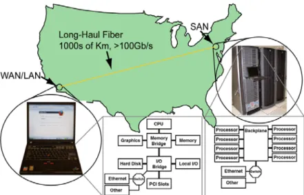
Modern high-speed communication is grouped primarily among wireless and wireline
channels. Wireless communication is currently comprised of cellular communication for
mobile telephony and broadband data communications using standards such as IEEE
802.11b/g [2]. Wireless data communications are expected to grow through the
deployment of WiFi networks and data services over cellular communication. While the
focus of recent investment and consumer demand has accelerated the development of
wireless infrastructure, the workhorse of data communication remains wireline
technology. Wireline networking is comprised of local area networks (LAN), storage area
networks (SAN), wide-area networks (WAN), and long-haul communication. These
divisions are focused on the distance and speed of the network.
Wireline communications are typically designed to support the highest data rates over
a physical channel. Optical fiber is the backbone of telecommunications networks around
the world. Optical fiber features extremely low loss over great distances and large
bandwidths. Protocols such as the Synchronous Optical Network (SONET) have
benchmarked the progression of optical communication networks [3]. Fiber-to-the-home
(FTTH) technologies extend this broadband access directly to the consumer, providing
data rates over 1Gb/s [4]. Current barriers for FTTH are economic, requiring bundling
data, voice, and video communication for consumers [5]. However, hardware costs, both
optical and electrical, account for a fifth of the installation cost [4].
Computing and communication circuit design have traditionally been treated
computational systems in SANs. Computer networking has stimulated data rate demands
in serial communication. Several different communication demands exist in computers.
First, the processor must communicate with peripheral RAM and other chips through the
memory bus as shown in Figure 1.1. As processor speeds have increased dramatically
over the past decades, more emphasis has been placed on the data rates of the serial link.
Chip-to-chip communications require data rates of nearly 1Gb/s over several centimeters.
While the serial link transceiver circuits have kept pace with the increase in processor
speed, the physical interconnect between the devices has changed very little. New bus
standards such as peripheral component interconnect (PCI) express have been adopted to
meet future bus needs in personal computers [8].
Larger computers such as servers and supercomputers consist of hundreds of parallel
processors. Blade cards have become prominent in server applications [6]. Midplane and
backplane serial communication connects the processors and cards in a rack mounted box
[7]. While these servers currently operate at 2.5Gb/s, backplane rates of nearly 10Gb/s
over distances of a meter are anticipated. Backplane interconnects have become the focus
of serial link research, as higher speeds are needed. However, signal attenuation,
dispersion, and connector reflections limits the bandwidth of these links. Recent protocols
that support high-speed backplane communication such as InfiniBand, Gigabit Ethernet,
and FibreChannel have been adapted to consider the signal integrity issues in high-speed
backplanes [9][10].
This thesis studies how timing issues, specifically deterministic jitter, can be overcome
so as not to impede high-speed wireline communication. Opportunities for developing
more sophisticated equalization for bandwidth-limited channels have not been fully
realized. In particular, understanding the generation of jitter in serial links provides means
for predicting the signal integrity problems that occur in wireline channels. Through the
analysis and modeling of jitter in bandwidth-limited interconnects, I develop methods for
determining bit-error rate (BER) performance as well as new types of equalization to
overcome bandwidth limitations.
1.1
Background: The Evolution of Serial
Communications
The role of serial communication is to transmit and receive information over a
channel. High-speed serial links are the input/output (I/O) interconnect between two
chips. Because of space and size constraints, the number of parallel serial links is often
limited, and the goal of circuit designers is to increase the speed at which each link
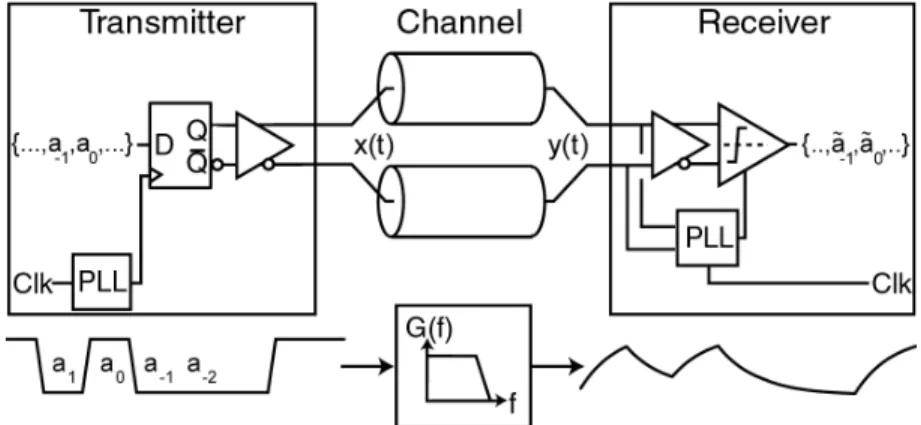
operates. The basic communication link is demonstrated in Figure 1.2. A transmitter takes
several parallel data paths and multiplexes them into a single serial data stream. The
transmit phase-locked loop (PLL) re-times each bit and drives them electrically or
optically over a fixed channel. At the receiver, two operations must be performed. First,
the signal must be amplified and detected to determine the appropriate transmitted bit.
Second, a receiver PLL must generate a sampling clock to determine when the bit
detection occurs. The serial stream is then demultiplexed into parallel data.
In the past, the channel environment could be, for the most part, ignored. The loss and
dispersion introduced by electrical interconnects was negligible because the bandwidth far
exceeded the data rates and, consequently, the data rates of high-speed links were limited
primarily by the speed of devices in a standard Silicon technology.
Early serial interfaces provided noise immunity through current integration [11]. As
rate demands increased, multiplexing was introduced to create a serial stream [12]. The
burden of these architectures was generating low jitter clock phases. These phases
oversampled the received data and detected the transition boundaries. More attention was
concentrated on the problems of timing jitter and circuits that produced low jitter while
providing time delay [13].
Delay-locked loop (DLL) circuits have favorable jitter attenuation properties [14] and
were enhanced using injection locking [15]. Interest in DLLs was spurred by limitations of
PLLs used for clock and data recovery (CDR) of optical signals. Jitter was reduced
through combining DLL and PLL circuits [16]. CDR designs for optical communication
were steadily taking advantage of new processes to reach the SONET rates [17]-[19].
Oversampling receivers migrated into new circuit technologies to reach the bandwidth
limitations (4Gb/s) of process technology [20]. However, the electrical interconnect in
these systems is not ideal and has a limited bandwidth. Once link speeds increased beyond
3Gb/s, circuit designers were forced to consider new techniques for managing signal
integrity in bandwidth-limited channels. Equalization was introduced to serial links both
in the transmitter and receiver to compensate for data degradation due to attenuation and
Pre-emphasis equalization amplifies the high-frequency signal components that are
attenuated by the channel. As link speeds became channel-limited, several integrated
circuit designs were proposed that introduced one- and two- tap amplitude pre-emphasis
[21]-[23]. However, amplitude pre-emphasis was limited by the need for some adaptation
for the channel behavior. Recent work has demonstrated backchannel adaptation through a
low frequency signal transmitted over the common mode of the differential lines [24].
This common mode technique is also referred to as “phantom” mode communication and
was proposed to reduce the wiring constraints of serial links [25].
In the receiver, new schemes implementing decision feedback equalization (DFE)
were introduced [26]. These schemes were adapted from early work on echo cancellation
caused by dispersion in optical fiber communications [27]. DFE designs have expanded to
allow for compensation over several bit periods and included adaptation schemes
[28][29].
Additionally, the data rate demand has increased interest in signaling beyond two-level
pulse amplitude modulations schemes (2-PAM). In particular, the use of quaternary
modulation such as four-level pulse amplitude modulation (4-PAM) was demonstrated in
[30][31]. These schemes sacrifice signal-to-noise ratio in integrated environments where
voltage scaling occurs with process migration. However, 4-PAM can achieve twice the
data rate with roughly the same bandwidth. A general description of serial link design for
channel-limitations and M-PAM communication is provided by Stojanovic [33].
The past decade has seen new approaches to the characterization of jitter through
measurement techniques. Early studies of jitter focused on digital transmission through
long haul fiber-optic networks [34][35]. Additionally, jitter became critical in the
performance of high-speed sampling circuits, in particular analog-to-digital conversion
[36]. In communication testing, the relationship between behavioral models of jitter and
measurement needed to be established accurately for low BER. Li and Wilstrup discussed
Subsequently, they established limitations on the accuracy of this jitter separation
[38][39]. The result of these new modeling efforts has been a jitter standard for
FibreChannel [40]. Currently, modeling work has attempted to refine the analysis of
sources of deterministic jitter [41] as well as to link jitter to the performance of frequency
references [42]-[45].
Advancing data rates requires attention to equalization techniques to handle the
bandwidth limitations of the channel. In this thesis, the effect of bandwidth limitation on
deterministic jitter characteristics is modeled and analyzed. The development of
equalization techniques for deterministic jitter promises to enhance the signal quality of
the communication over these channels while offering low power implementations.
1.2
Organization
This thesis describes timing jitter in high-speed communication links. In Chapter 2
signal integrity is discussed in the context of bandwidth limited systems. Bandwidth
limitation introduces strong deterministic impairments to the data sequence that are
compounded by random noise sources. The predicted bit errors due to timing and voltage
errors are demonstrated, and the sources of random jitter in modern high-speed links are
discussed. Additionally, the relationship between the deterministic jitter and the
performance of high-speed PLLs is discussed.
In Chapter 3 deterministic timing deviations correlated to the data sequence
[data-dependent jitter (DDJ)] are analyzed, and expressions for the threshold crossing
times are derived for several different types of linear time-invariant (LTI) channels.
Additionally, DDJ in quaternary signaling is discussed. The general expression of the
threshold crossing times is useful for introducing a Markov model for the progression of
the threshold crossing times and calculating time domain behavior such as cycle-to-cycle
Chapter 4 introduces a novel technique for compensating the data-dependent jitter
introduced in bandwidth-limited channels. This equalizer leverages the unique
relationship between the data sequence and the threshold crossing time to reposition the
transition edge. Two circuits are presented in this chapter to correct DDJ. The first is built
into a clock and data recovery circuit. The second compensates rising and falling edges
individually in situations where the signal response is not linear.
The use of data-dependent jitter equalizers is not restricted to the receiver, and Chapter
5 discusses the design and implementation of a phase pre-emphasis scheme that can
augment the performance of amplitude pre-emphasis. Phase pre-emphasis introduces a
timing deviation to the data edge before the signal is transmitted, with the assumption that
the channel response will correct the timing. This technique is particularly interesting
because phase pre-emphasis is not subject to error propagation in the receiver and does not
require large power consumption.
In Chapter 6 the role of crosstalk on jitter is introduced. Crosstalk couples unwanted
energy between adjacent serial links. The relationship between crosstalk and deterministic
signal jitter is discussed and compared for different data modulation schemes. Chapter 7
employs the derived relationship between the crosstalk-induced jitter and the occurrence
of signal transitions on neighboring lines to remove this source of jitter. Hardware results
are presented for a complementary metal-oxide semiconductor (CMOS) process, and the
testing demonstrates that a crosstalk-induced jitter equalizer can drastically improve the
timing margins of the data eye.
Finally, Chapter 8 introduces a new architecture for submillimeter integrated radios.
The technology scaling in Silicon Germanium (SiGe) has pushed device speeds into
submillimeter frequencies. Consequently, the integration of entire radios including signal
generation, a power amplifier, and an antenna is possible on a single chip. Furthermore,
the small wavelengths at submillimeter frequencies provides a unique opportunity to
discusses the frequency generation and distribution problems for fully integrated
submillimeter phased array transmitters. The design uses a coupled oscillator array which
places oscillators at each element of the array. To generate a coherent phase, each
oscillator is locked to a neighboring oscillator. Driving the array with a low-phase noise
external master reduces the phase noise across the entire array. Hardware results in a SiGe
Chapter
2
Signal Integrity in
Broadband
Communications
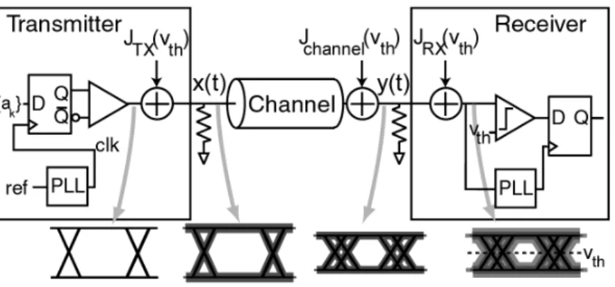
Signal integrity is a metric for discussing the achievable bit error rate (BER) of a communication link. This chapter discusses signal integrity and the impact of timing jitter.
The architecture of a broadband communication system involves three principle components as illustrated in Figure 2.1. The first component is a transmitter that generates
a data signal. The signal at the output of the transmitter is denoted x(t). Typically, the transmitted digital signal consists of two amplitude levels, generally called two-level pulse
amplitude modulation (2-PAM), representing the one or zero bit, ak. When the bits are transmitted for one bit period, 2-PAM is referred to as a non-return-to-zero (NRZ) signal.
The second component is a communication channel over which the data propagates. This channel can be wireless or wireline. For broadband signal transmission over wireline
channels, the channel bandwidth has the low-pass response, G(f), shown in the figure. After the signal has passed through the channel, it is distorted by the channel and is
denoted y(t). Finally, the third component is a receiver that detects the data signal and recovers the transmitted bits. Each block is designed to operate in a particular channel
environment. In this chapter we describe the operation and jitter generation of each of these blocks.
2.1
Shannon’s Theorem
Claude Shannon formalized the ultimate limit of capacity in communication channels
in his seminal paper [46]. The implications of this work directed communication theory and formed the foundations of information theory by establishing a relationship between
signal-to-noise ratio (SNR), channel bandwidth, and communication capacity. The Shannon limit is given by the channel capacity, C, and is
, (2.1)
where BW describes the bandwidth of the channel, Psignal is the signal power, and Pnoise is the noise power. The channel capacity in (2.1) assumes that the communication channel is
linear and that the noise is additive. The ratio of the signal and noise power is referred to as the signal-to-noise ratio (SNR). For large SNR, the capacity is much greater than the
channel bandwidth.
In practice, designing high-speed circuits that operate at data rates much greater than
the channel bandwidth is difficult. Shannon’s Theorem demonstrates the communication capacity, while circuit designers must develop clever methods to realize this capacity.
Examining conventional digital communication schemes builds appreciation of these challenges.
2.1.1 Signal Power
For NRZ signals, each binary symbol is transmitted over a bit period, T. For an uncoded data sequence, each symbol is uncorrelated to adjacent symbols. Therefore, the
data symbol, ak, satisfies the convolution property, [47]. Consequently, the autocorrelation of the NRZ signal is expressed as
C BW log2 1 Psignal
Pnoise
---+
⎝ ⎠
⎜ ⎟
⎛ ⎞
⋅ =
an⊗a
, (2.2)
where Vs is the signal swing. The power spectral density (PSD) for this autocorrelation is calculated with the Fourier transform:
. (2.3)
In Figure 2.2, the PSD of (2.3) is illustrated. The plot of Sxx(f) indicates that the power is concentrated at frequencies below 1/T. The total power that reaches the receiver is limited by the low-pass bandwidth of the channel. For a low-pass transfer function, G(f), with bandwidth, BW,
. (2.4)
This result gives the power of the signal at the receiver required to determine (2.1).
Rxx( )τ Vs2 1
τ
T
---– T>τ≥–T
0 τ≥T,τ<–T
⎩ ⎪ ⎨ ⎪ ⎧ =
Sxx( )f ℑ{Rxx( )τ } Vs2T sin(πfT)
πfT
---⎝ ⎠
⎛ ⎞2
= = V
2
Hz
---Figure 2.2 Power spectral density of the NRZ data sequence and white noise.
Psignal 2 Sxx( )f G f( )2df
0
∞
∫
2.1.2 Noise Power
Noise is inevitable in any electronic system and exhibits a different PSD than the signal. For an additive white noise source, the autocorrelation of the noise is
, (2.5)
demonstrating that the noise is uncorrelated. Therefore, the noise PSD is
. (2.6)
The noise PSD is superimposed with the signal PSD in Figure 2.2. The noise power is
cal-culated by integrating (2.6):
. (2.7)
Returning to (2.1), the signal and noise power are functions of the bandwidth. The
inte-grated power of the noise increases linearly with bandwidth while the inteinte-grated signal power in (2.4) falls off. Finally, the SNR is
. (2.8)
The SNR can be evaluated with a model of the communication channel transfer function.
2.1.3 Bandwidth
The bandwidth directly improves the capacity in (2.1) and affects the SNR in (2.8). Bandwidth is useful for limiting noise in the link, but, more recently, data rates in
high-speed serial links are restricted by the bandwidth. While the bandwidth in optical communication systems is tailored to maximize (2.8), bandwidth in serial links is fixed by
frequency dependent attenuation and reflections in the transmission line and connectors.In
Rnn( )τ No
2 ---δ τ( ) =
Snn( )f No
2 ---= V 2 Hz
---Pnoise No G f( )2df
0
∞
∫
[ ]V2=
SNR Psignal Pnoise
--- Vs
2
No
---2T sin(πfT)
πfT
---⎝ ⎠
⎛ ⎞2
G f( )2df
0
∞
∫
G f( )2df
Figure 2.3, ideal low-pass responses are plotted. The higher-order filters approach the
limit of the “brick-wall” filter, ideal for filtering the noise PSD demonstrated in Figure 2.2. Once the signal PSD falls below the noise PSD, the response should attenuate
the noise to maintain the SNR. In optical receivers, the bandwidth of the receiver is often chosen to be around 70% of the bit rate [53]. Higher bandwidths become noise-limited,
while lower bandwidths reduce the signal energy. In the following sections, bandwidth limitations of high-speed optical and electrical channels are reviewed.
2.1.3.1 High-Speed Serial Links
Currently, data rates in high-speed serial links are impeded by bandwidth-limitation. High-speed serial links are designed with transmission line channels that connect the
input/output (I/O) between different chips. A shielded cable is a simple serial link. In servers and parallel computers, a backplane, shown in Figure 2.4, provides I/O between
different boards. Two peripheral boards are connected to the backplane through high-speed connectors. The differential transmission line starts at one chip and is routed
through the peripheral boards and backplane. The transmission lines have vias created by fabricating the transmission lines from one layer to another layer. Thus, the backplane link
contains the impedance discontinuities introduced by the vias and connector. Complete
shielding is not possible due to the routing density and several serial links run in parallel.
Shielded transmission lines are limited by skin-effect losses and dielectric losses. Skin
effect arises from non-uniform electric field in conductors. Consequently, the resistance of the wire increases and is accompanied by an effective internal inductance [51]. The skin
loss can be expressed as
, (2.9)
where l is the wire length, µ is the permeability, and σ is the conductivity. The loss is a
function of frequency, which is why it is generally referred to as a frequency-dependent
loss. The phase shift and amplitude attenuation are identical for skin effect.
Additionally, the dielectric material of the FR4 material causes loss:
, (2.10)
where εr is the dielectric constant and tanδ is the loss tangent of the material. A thorough
discussion of the skin and dielectric losses in modern materials is given by Deutsch [52].
Gskin( )f = e–(1+j)l πµσf
Figure 2.4 FR4 backplane with peripheral boards and connectors for serial communication.
Gdielectic( )f e
l εrtanδ c
---f
–
The via stubs and connectors cause signal reflections at gigahertz frequencies. These
reflections also cause dispersion and, consequently, intersymbol interference in the link. In Figure 2.5, the FR-4 frequency response features bumps that are attributable to these
reflections. Finally, the connectors and parallel transmission lines in the backplane can generate crosstalk between neighboring lines. The crosstalk also limits the bandwidth.
For modern backplanes, these loss and dispersion mechanisms limit the bandwidth of interconnects to around 3GHz. Consequently, the bandwidth is fixed, and the challenge for
circuit designers is to reach higher data rates through equalization, different modulation schemes, and coding.
2.1.3.2 Optical Links
Optical fiber represents broadband channel that may replace electrical interconnects. The loss of fiber is low over a wide range of optical frequencies. At the 1.55µm
wavelength, the loss of 0.2dB/km extends over 10THz. In principle, this window could support a data capacity of 4 Tb/s [54]. However, in long-haul fiber-optic communication
dispersion limits the modulation frequency and the optical bandwidth is split into 10Gb/s
channels using wavelength-division-multiplexing (WDM). Reaching 40Gb/s is possible if fiber dispersion is controlled.
The origins of dispersion depend on the fiber [55]. Initially, fibers were designed with large fiber diameters (50-100µm). As light propagates down the fiber, it reflects off the
fiber walls randomly. The different path lengths cause modal dispersion given by the range of arrival time for the optical signal, ∆T:
, (2.11)
where L is the fiber length, c is the speed of light, and ncore and ncladare the index of refraction of the cladding and the core. Over 1km of fiber, this dispersion is greater than
100ps. In response, fiber manufacturers developed single mode fiber with a narrower core (8-10µm).
Next, the modulated signal suffers from a group-velocity dispersion, characterized by the variation in the group velocity variation, D. The amount of dispersion depends on the modulation bandwidth and, hence, the data rate. Group velocity dispersion is given by
, (2.12)
where the modulation bandwidth is the range of wavelengths, ∆λ.
Finally, optical bandwidth is limited by polarization mode dispersion. The modulated
light is composed of two polarizations that propagate at different speeds. This causes a statistical spread in the arrival time due to the time-varying coupling between modes:
, (2.13)
where Dpmdis the polarization mode dispersion.
Tremendous optical bandwidth exists, but the design of optical transceivers above
10Gb/s must consider the use of electronic as well as photonic equalization techniques for lightwave communication [56].
∆T ncore–nclad
8c n⋅ core
---⎝ ⎠
⎜ ⎟
⎛ ⎞2
L
=
∆T = D ⋅∆λ⋅L
2.1.4 Capacity
In Figure 2.6, the channel capacity is plotted against the bandwidth of the Butterworth filters in Figure 2.3. The NRZ PSD is constant, i.e., the bit rate is fixed. Increasing or
decreasing SNR shifts the capacity curves vertically. Notably, most of the capacity improvement occurs when using a second-order response over a first-order response. The
channel capacity typically reached in high-speed systems is shown for comparison. Here the (3dB) cut-off frequency, fc, is 70% of the bit-rate, fb. The margin between the achievable capacity and the actual data rate is lost to preserve simplicity in system and circuit design. Shannon provided a limit for communication capacity. However, this
theory does not offer insight into how to design circuits for a communication link. As high-speed serial links are increasingly bandwidth-limited, communication theory
suggests appropriate modulation schemes and equalization techniques to reach the channel capacity limit [47]. For instance, maximum-likelihood sequence estimation can
ideally recover an extremely distorted or bandwidth-limited signal. In high-speed integrated circuit design, the possible implementations are curtailed dramatically, and
circuit designers must rely on a subset of the signal processing tools to maximize data rates. The computational power required by many equalization techniques is unrealizable
both from the standpoint of power as well as circuit speed. Early equalization of
bandwidth-limited channels focused on data transmission over the legacy Bell telephone network [50]. In the following section the signal integrity of communication in the
bandwidth-limited region is discussed. The impact of the bandwidth limitation on the signal motivates the analysis of deterministic effects and equalization techniques
introduced in later chapters.
2.2
High-Speed Signal Integrity
2.2.1 Bit Detection
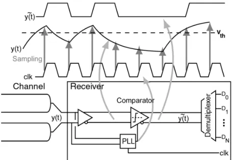
A common receiver scheme is to detect the digital data stream through sampling the input analog signal as illustrated in Figure 2.7. First, the input signal, y(t), is amplified and filtered. Next, the comparator makes a decision about the value of the analog signal by comparing the value to a voltage threshold, vth. This decision is made with the sampling clock signal, clk. Once the comparator samples the analog data signal, the result, , is interpreted as the digital symbol, either 0 or 1 for 2-PAM.
Hence, the analog signal must surpass the voltage threshold at the sampling time to detect the bit without error. The actual implementation of a comparator places more
Figure 2.7 Digital regeneration through sampling of the analog signal in a comparator.
restrictions on the analog signal swing. The comparator has metastability issues for small inputs and, consequently, the signal swing must typically significantly surpass the voltage
threshold for proper operation. Additionally, for small signal swings, the comparator needs a certain amount of hold time during which the analog signal remains above the
voltage threshold to generate the proper digital value. The comparator requires a minimum voltage and timing margin on the signal to operate without generating additional errors.
To gauge the average voltage and timing margins, the signal is folded every bit period to create an overlapping set of possible signal voltages. This is a data eye, so called
because the center of the plot is open, determining the voltage and timing margins with respect to the sampling clock. The data eye facilitates calculating the bit-error rate (BER)
from the signal. Consequently, the data eye will provide qualitative and quantitative definitions for the signal integrity of the analog signal. An example of a data eye is shown in Figure 2.8 for a first order system. The voltage margin is ∆V and the timing margin is ∆T. Each is respectively defined at a sampling time and voltage threshold.
2.2.2 Voltage and Timing Margins
In this section the deterministic effects of bandwidth limitation on eye closure are discussed. Lowering the bandwidth or increasing the bit rate reduces the eye opening,
aggravating the detection of digital symbols from the analog signal. Since bit-by-bit signal detection requires a sampling clock and a voltage threshold, signal integrity is defined as
the relationship of the voltage and timing margins of the data eye to a bit-error rate (BER).
The threshold crossing time at which the analog signal passes the voltage threshold is
denoted, tc, i.e. y(tc)=vth. Part of the contribution of this thesis is the analysis of the threshold crossing time deviations, which will be discussed in the next chapter. For LTI
responses, the voltage threshold occurs where the timing margins are the greatest. The fastest edge on the left and right side of the eye data are identical, and the timing margin is
. (2.14)
The optimal sampling time is chosen to minimize errors. The timing margin given by
(2.14) determines the sampling time. Equally spacing the sampling time between the slowest and fastest edges gives
. (2.15)
Now, the voltage margin is defined from this sampling time. Alternatively, the voltage margin could be maximized to determine the sampling time:
. (2.16)
Equations (2.14) and (2.15) are worst-case definitions of the voltage and timing margins.
In many cases, the worst-case is too severe in communication applications because a small BER might be acceptable. Finding the margins for a given BER is possible by studying the
probability for the deterministic features of the signal.
2.2.3 Modeling of Intersymbol Interference and Data-Dependent Jitter
Intersymbol interference (ISI) reduces the voltage margins of the data eye from the
maximum swing. The voltage margins achieved in (2.16) are a subset of the actual logical values. If the maximum voltage swing is 2Vs, the peak-to-peak reduction due to ISI is
. (2.17)
∆T = T–(tc slow, –tc fast, )
ts tc slow, ∆T
2
---+ T
2
--- tc slow, +tc fast, 2
---+
= =
∆V = vs max, –vs min,
Since the margins depend on the precise sampling time, the ISI is only meaningful for a
particular sampling time. The deterministic reduction in the timing margins due to
band-width is peak-to-peak data-dependent jitter (DDJ) and from (2.14) is
. (2.18)
The definition for jitter is only meaningful at a particular voltage threshold. The
peak-to-peak reduction in the timing and voltage margins is shown in Figure 2.9 as a func-tion of the bandwidth of a first-order channel. The eye opening is normalized both in the
voltage domain as well as the timing domain. At larger bandwidths the ISI is the dominant constraint. As the bandwidth reaches about fc=0.3fb, the DDJ increases and the timing margins become restrictive. Once fc = 0.11fb, the eye becomes completely closed for a first-order system and the voltage and timing margins go to zero. Therefore, in extremely
bandwidth-limited situations, understand the timing and voltage degradation is important.
To understand the relationship of ISI and DDJ on non-zero BER, modeling the
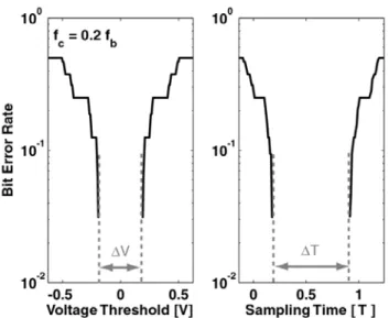
worst-case trajectories predicts probabilistically how often these margins are reached. A “bathtub” curve is the BER cumulative-distribution function (CDF) and is shown in
Jpp DDJ, = T–∆T
Figure 2.10, where a data eye is scanned at different voltage thresholds and sampling
times and the bit-errors are counted.
Since signal integrity is defined for a specific BER, a distinction between peak-to-peak
performance and the performance at a given BER is necessary. If we were satisfied with an error of 10-1, the margins would be expanded significantly. In serial links errors are
tolerable, if they ever occur. Typically, we are ultimately interested in the signal integrity for 10-12 BER. In practice, simulating the response for 1012 bits is difficult and, hopefully,
unnecessary. For deterministic effects, the worst-case scenarios occur more regularly. Simulating n-bit sequences captures the relevant deterministic reduction in the BER if the reduction in the margins occurs with n bits.
The CDFs in Figure 2.10 suggest modeling the ISI and DDJ with an ad hoc probability density function (PDF). The step gradient along the bathtub edges suggest modeling the PDFs for ISI and DDJ as a combination of dirac delta functions:
, (2.19)
Figure 2.10 Cumulative distribution function for BER for DDJ and ISI in the absence of random noise. The margins are the gap in the center of each bathtub.
PDFISI( )vs 1
2k
--- δ(vs–vi) and PDFDDJ( )tc 1
2k–1
--- δ(tc–ti)
i= 1 2k–1
∑
=
i =1 2k
∑
where the sampled voltage, vs, and threshold crossing time, tc, occur at each delta function located at voltages, vi, and threshold crossing times, ti, which are determined by the partic-ular data sequence that is k bits long. The number of peaks in (2.19) depends on k. Notably there are 2k-1 threshold crossing times, but 2k voltages. Bandwidth limitations tend to
increase the number of dominant PDF peaks. In many cases several threshold crossing time delta functions overlap into a single DDJ peak, providing a more compact the PDF
than in (2.19). The simplest form of DDJ occurs when two peaks are present:
. (2.20)
This PDF is sometimes called the absolute jitter since it is compared to an ideal reference. The purpose of Chapter 3 is to investigate the location of these peaks. Given the DDJ PDF,
we can analyze some statistical properties. We can calculate the mean, mDDJ, and vari-ance, (σDDJ)2, of (2.20). From measurements, the root-mean-square (rms), Jσ, is σDDJ, and we use J to imply jitter. The rms jitter will be used in subsequent sections to calculate BER. Jpp gives the absolute range for the transition arrival. From (2.20), the rms and peak-to-peak DDJ is
. (2.21)
pdfDDJ( )tc 1
2
--- δ tc–t
o
( ) δ tc–t
o–tc DDJ,
( )
+
[ ]
=
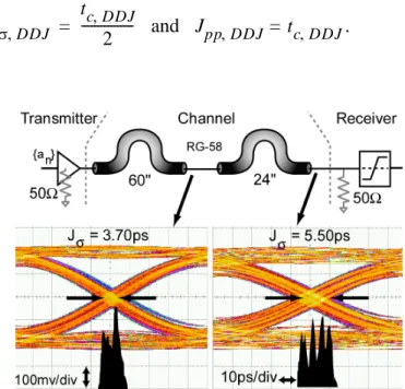
Figure 2.11 The data-dependent jitter generated over RG-58 cable at 10Gb/s and jitter histograms.
Jσ,DDJ tc DDJ,
2
--- and Jpp DDJ, = tc DDJ,
To illustrate the impact of DDJ on a real data eye, Figure 2.11 demonstrates a 10Gb/s data sequence transmitted over RG-58 cable. The cable bandwidth reduces with increasing
length. After 60” of cable, the data suffers from both ISI and DDJ. The total rms jitter is 3.70ps after 60” and increases to 5.50ps after transmission over an additional 24”. The
additional length reduces the bandwidth of the link and increases the jitter. Qualitatively, the DDJ in the two eyes justifies the delta function model. In the first plot the jitter has two
dominant peaks. In the second plot four distinct peaks appear. However, these peaks are obscured by random jitter which we will now discuss.
2.2.4 Random Noise and Jitter in Bit Error Rate
This section discusses the impact of random, or non-deterministic, sources of noise on the link performance. Noise is an inevitable feature of any electronic system. Johnson and
Nyquist determined that the thermal noise resulting from a resistance behaves as uniform power spectral density (PSD) [48][49]. Heffner demonstrated that any resistance resulted
in a PSD that was essentially flat to 80THz [57].The PSD for a resistance is
, (2.22)
which resembles our noise PSD assumption in (2.6). Uhlenbeck and Ornstein
demon-strated that any bandlimited thermal process is modeled with a Gaussian PDF [58]. In electrical interconnects we assume that bit detection is limited by Gaussian noise
pro-cesses. A general Gaussian PDF describing the voltage noise is given as
, (2.23)
where . Random noise increases the probability of error. The voltage noise is added to the signal, creating a possibility that the bit is detected incorrectly. The
probabil-ity of an error is expressed as the combination of the probabilprobabil-ity that the signal will be detected as a one when a zero was transmitted and vice versa [47]:
Sr( )f = 4kTR V
2
Hz
---PDFn( )v 1
2πσn2 ---e
v2
2σn2
---⎝ ⎠ ⎜ ⎟ ⎛ ⎞
–
=
. (2.24)
In most situations, Pr(0)=Pr(1)=1/2, and the PDF is expressed with (2.23):
. (2.25)
To express the BER, (2.25) is multiplied by the rate at which bits are transmitted, which is 1/T for NRZ transmission. In high-speed digital communication, the finite rise and fall times introduce timing jitter. Random jitter can be described as a translation of the voltage noise into timing deviations through the signal slope [59]:
. (2.26)
The threshold crossing time deviation, RJ, due to voltage noise is also a random variable. This expression relies on an implicit relationship between the slope “near” the threshold crossing time and the actual threshold crossing time. The perturbation due to noise is
assumed to be small. This type of random timing jitter in digital signals is clearly a bounded distribution since the rise and fall time of the transition is finite while the voltage
noise is unbounded. Nevertheless, the analysis of random jitter will be approached as the
Pr error( ) = Pr(1 0)Pr( )0 +Pr(0 1)Pr( )1
Pr error( ) 1
2 --- 1
2πσn2 --- e
v+vs
( )2
2σn2 ---⎝ ⎠ ⎜ ⎟ ⎛ ⎞ – v d vth ∞
∫
ev–vs
( )2
2σn2 ---⎝ ⎠ ⎜ ⎟ ⎛ ⎞ – v d ∞ – vth
∫
+ ⎝ ⎠ ⎜ ⎟ ⎜ ⎟ ⎜ ⎟ ⎜ ⎟ ⎛ ⎞ =Figure 2.12 Random noise and jitter distributions and their relationship to the data eye.
RJ t( )c n t( ) x′( )to