Abstract- This paper deals with the design and analysis of folded cascode operational transconductance amplifier in different regions of operations: strong, weak and moderate inversion region. The folded cascode OTA consists of cascode OTA and cascode gain boosting technique. By using 0.35µm technology, the simulation shows DC gain of 78.42dB with a unity gain bandwidth of 446.07 MHz and power consumption of 412.77µW in strong inversion mode. The moderate inversion mode has a DC gain of 93dB and it provides unity gain bandwidth of 75.64MHz with a power consumption of 23.72µW. In weak inversion mode, it has 76.84dB DC gain with a unity gain bandwidth of 19.46 MHz and a power consumption of 0.1µW.
Keywords:Operational Transconductance Amplifier, CMOS analog integrated circuits
1. Introduction
The operational transconductance amplifier is an op-amp without an output buffer so it can drive only loads .It is also called as voltage controlled current source (VCCS) because its differential input voltage produces an output current. OTA is the important building block in analog circuits. It faces many difficulties in low voltage design providing low power consumption and high gain [2]. To improve the gain, cascoding of transistors is not possible for low voltage design due to its output swing limitation. The current equation of OTA signifies that the transconductance of OTA strongly depends on the bias current [3] and is given by
Io = Gm {V (+) – V (-)} (1)
Besides, there are also other methods to enhance the OTA gain, e.g. a use of replica amplifier and positive feedback. Among all these methods gain boosting technique is used in the paper as it provides high gain and high unity gain bandwidth with low power consumption [3] as compared to other methods.
2. Folded Cascode OTA Architecture
2.1.Input Stage
The input stage is a differential input that converts the input voltage to current. As NMOS devices have greater mobility so here NMOS differential pair is taken as input source [1].
2.2. Analysis of folded cascode OTA architecture
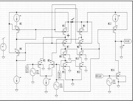
The basic configuration of each circuit consists of operational amplifier. The Fig.1 shows the folded cascode OTA (the name folded cascode OTA comes from folding down p-channel cascode active loads of a differential pair and changing the MOSFETs to n-channels. There are many configurations of OTA’s but folded cascode op-amp is opted because of its high bandwidth and large gain. Also this OTA has good PSRR compared to the two stage op-amp since the OTA is compensated with active loads [1].
Figure 1: Folded Cascode OTA architecture
The operation of folded cascode consists of one differential pair consisting of NMOS transistors M1 and M2.MOS transistors M3 and M4 provide the DC bias voltage to M5, M6, M7, M8 transistors [1]. The gain of the folded cascode OTA is given by
Vout/Vin =Gm1R0 (2)
GBW= Gm1/CL (3)
Where, Gm1 is the transconductance of the transistor M1 and R0 =(R looking into drain of M10)//(R looking into drain
of M8).
3. Design Procedure of Folded Cascode OTA by using Gm1/ID Technique
The folded cascode op-amp is characterized by performances like DC gain, unity gain bandwidth, noise and power [2]. These measures are fixed by various parameters like transistor biasing, bias current, supply voltage and other values. 3.1. Design flow
The Gm/ID technique consists of different steps from which the high DC gain and high bandwidth can be achieved. The
formulation of design flow clarifies a top-down synthesis methodology for CMOS folded cascode OTA architectures in Fig.2 [1].
Figure 2: Design flow of folded cascode OTA [1] 3.2. Design in Strong Inversion Region
In this region of operation Gm/ID ratio decreases as a function of current. It is concluded that the sizes found in
strong inversion region are more important than other regions; this can be explained by using high current values towards other regions [2]
.
After applying the design strategy clarified previously, the design parameters in strong inversion region can be summarized in Table 1.Table 1: Design parameters in strong inversion region.
Parameters Values ID(µA) 55 W1,2(µm) 3.5 W9,10,11,12(µm) 3.5 W3,4(µm) 8.75 W5,6,7,8(µm) 8.75 W13(µm) 29.99 W14(µm) 17.75
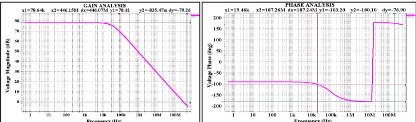
The folded cascode OTA has a gain of 78.42dB with a unity gain bandwidth of 446.07 MHz and phase margin of 76.96deg with power consumption of 412.77µW as shown in fig .3.
Figure 3: Folded Cascode OTA’s gain & phase curve in strong inversion region
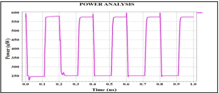
The curve described the dynamic power consumed by the circuit is shown in fig. 4.
Figure 4: Power Consumption in strong inversion region
The folded cascode OTA consumes average power of 412.77 µW. The maximum and minimum power consumed by the folded cascode OTA is 598.22 µW and 226.51 µW respectively.
3.3. Design in Weak Inversion Region
Even with smaller current values, weak inversion region presents higher Gm/ID values. The design parameters found are
represented in Table 2 for weak inversion region. The bias current used in weak inversion region is only 0.1µA.
Table 2: Design parameters in weak inversion region.
Parameters Values ID(µA) 50nA-0.1µA W1,2(µm) 6.25 W9,10,11,12(µm) 3.5 W3,4(µm) 12.625 W5,6,7,8(µm) 15.625 W13(µm) 27.99 W14(µm) 6.25
After applying the design strategy we obtain the results of gain, unity gain bandwidth, and transconductance and power consumption as described in Table 3.
Table 3: Results for weak inversion region.
Specifications Values AV(dB) 76.84 GBW(MHz) 19.46 Transconductance(µS) 5.15 CL(fF) 10 Channel length(µm) 0.35 Power consumption(µW) 0.1088
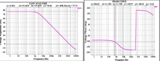
The folded cascode has a gain of 76.84dB with unity gain bandwidth of 19.46MHz with a supply voltage of 1V are plotted in fig.5.
Figure 5: Folded cascode OTA’s gain & phase curve in weak inversion region
The curve described the dynamic power consumed by the circuit in weak inversion region is shown in fig.6.
Figure 6: Power consumption in weak inversion region
The folded cascode OTA consumes average power of 0.1088µW. The maximum and minimum power consumed by the folded cascode OTA is 89.6533 µW and 0.1914 µW respectively.
3.4. Design in Moderate Inversion Region
In weak inversion region even with very low power consumption improved performance has been achieved and in order to further improve unity gain bandwidth, the folded cascode OTA circuit in moderate inversion region [1-2] is analyzed. The design parameters of moderate inversion region are given in Table 4.
Table 4: Design parameters in moderate inversion region.
Parameters Values ID(µA) 4µA W1,2(µm) 3.5 W9,10,11,12(µm) 3.5 W3,4(µm) 10.5 W5,6,7,8(µm) 10.5 W13(µm) 30.99 W14(µm) 3.5
gain of 93dB with unity gain bandwidth of 75.64MHz with a supply voltage of 2V as shown in fig.7
Table 5: Results for moderate inversion region.
Specifications Values AV(dB) 93 GBW(MHz) 75.64 Transconductance(µS) 74.12 CL(pF) 0.1 Channel length(µm) 0.35 Power consumption(µW) 23.72
Figure 7: Folded cascode OTA’s gain & phase curve in moderate inversion region
The curve described the dynamic power consumed by the circuit in moderate inversion region is shown in fig.8.
Figure 8: Power consumption in moderate inversion region
The folded cascode OTA consumes average power of 23.721140 µW. The maximum and minimum power consumed by the folded cascode OTA is 40.2857 µW and 7.1624 µW respectively.
4. Comparison of Results
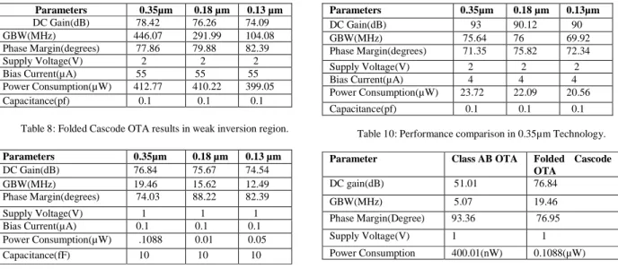
After discussing various parameters in different regions of operation, we compare our results study with other technology nodes i.e. 0.18µm and 0.13µm. The comparisons are given in Table 7, 8 and 9. It is clearly seen that with folded cascode OTA architecture, low power and high gain has been achieved.
5. Conclusions
Design of OTA is important in integrated continuous time filters. A folded cascode operational amplifier is designed and optimized in 0.35 µm CMOS technology. The transistor channel widths are optimized to get high unity gain
Parameters 0.35µm 0.18 µm 0.13 µm DC Gain(dB) 78.42 76.26 74.09 GBW(MHz) 446.07 291.99 104.08 Phase Margin(degrees) 77.86 79.88 82.39 Supply Voltage(V) 2 2 2 Bias Current(µA) 55 55 55 Power Consumption(µW) 412.77 410.22 399.05 Capacitance(pf) 0.1 0.1 0.1
Table 8: Folded Cascode OTA results in weak inversion region.
Parameters 0.35µm 0.18 µm 0.13 µm DC Gain(dB) 76.84 75.67 74.54 GBW(MHz) 19.46 15.62 12.49 Phase Margin(degrees) 74.03 88.22 82.39 Supply Voltage(V) 1 1 1 Bias Current(µA) 0.1 0.1 0.1 Power Consumption(µW) .1088 0.01 0.05 Capacitance(fF) 10 10 10 Parameters 0.35µm 0.18 µm 0.13µm DC Gain(dB) 93 90.12 90 GBW(MHz) 75.64 76 69.92 Phase Margin(degrees) 71.35 75.82 72.34 Supply Voltage(V) 2 2 2 Bias Current(µA) 4 4 4 Power Consumption(µW) 23.72 22.09 20.56 Capacitance(pf) 0.1 0.1 0.1
Table 10: Performance comparison in 0.35µm Technology.
Parameter Class AB OTA Folded Cascode
OTA DC gain(dB) 51.01 76.84 GBW(MHz) 5.07 19.46 Phase Margin(Degree) 93.36 76.95 Supply Voltage(V) 1 1 Power Consumption 400.01(nW) 0.1088(µW) References
[1] Daoud Dammak.H, Bensalem.S , Zouari.S and Loulou.M, “Design of Folded Cascode OTA in Different Regions of Operation through gm/ID” , World Academy of Science ,Engineering and Technology,pp28-33 2008.
[2] Soni.H, Dhavse.N, “Design of Operational Transconductance Amplifier using 0.35µm technology”, International Journal of Wisdom Based Computing vol 1, pp28-31, 2011.
[3] Razavi.B, “Design of Analog CMOS Integrated Circuits”, publisher McGraw-Hill, 2000.
[4] Luzzi.R, Pennisi.S, Scotti. G, Trifiletti.A, “2V CMOS Current Operational Amplifier with high CMRR”, European conference on Circuit Theory and Design, vol1, pp1/27-1/30, 2005.
[5] Bouzerara. L, Belaroussi. M.T, “Low Voltage, Low Power and High Gain CMOS Operational Tansconductance Amplifier ”,IEEE International
Symp. on Circuits and Systems,vol1,pp1325-1328, 2002.
[6] Daoud.H, Salem.S.B, Zouari.S, Loulou, “Folded Cascode OTA Design for Wide Band Applications”, International Conference on Design and
Test of Integrated Systems in Nanoscale Technology, pp437-440, 2010.
[7] Soni.P, Singh.B.P, Bhardwaj, “Design of OTA based Floating Inductor”, International Conference on Devices and Communications,pp1-4, 2008.
[8] Hasan.S.A , Hall.S, Marsland. J.S, “A Proposed Sub-threshold OTA-C Filter for Hearing Aids”, IEEE Conference on New Circuit and System conference, pp414-417, 2011.
[9] Suadet. A, Thongleam.T, Kasemsuwan.V, Vichienchom.K, “A 0.5 Volt Rail to Rail CMOS Pseudo-Differential OTA Using Simple Feed-
forward Technique”, International Conference on ECTI-CON, pp106-109, 2011.
[10] Li.Y.L.Han. K.F.Tan.X. Yan.N. Min.H, “Transconductance enhancement method for operational transconductance amplifiers, vol.46, No.19, pp1321-1323,2010.
[11] Antreich. K.J, Graeb.H.E, Wieser.C.U, “Circuit analysis and optimization driven by worst-case distances”, IEEE Trans. Computer Aided DesignVol.13,No.1,pp57-71,2002
[12] Dharchoudhury.A, Kang. S.M “Worst-case analysis and optimization of VLSI circuit performances,” IEEE Trans. Computer Aided Design