Arm Balancing Control and Experimental
Validation of a Grid Connected MMC with
Pulsed DC load
M. Jankovic,
Member, IEEE, A. Costabeber,
Member, IEEE,
A. Watson,
Member, IEEE, and J. C. Clare,
Senior Member, IEEE
Abstract—This paper focuses on the operation of a grid connected Modular Multilevel Converter (MMC) supplying a pulsed DC load. The goal is to achieve minimum AC power fluctuation despite the high power fluctuation present on the DC side. The MMC has been selected for its inherent ability to decouple AC and DC current controllers. How-ever, if no additional provisions are taken, the pulsed load causes imbalance of cell capacitor voltages between upper and lower arm in each phase. The paper presents the the-oretical analysis of the imbalance problem, and proposes a simple arm balancing controller to enable the operation of the converter under pulsed DC load. The effectiveness of the controller has been successfully verified on a 7kW
MMC experimental prototype with a 3kApulsed DC load.
Index Terms—Arm balancing control, Grid-connected converter, Modular Multilevel Converter, Pulsed power.
I. INTRODUCTION
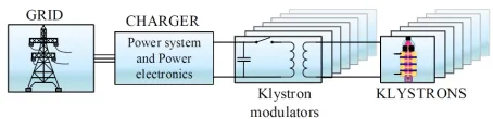
Modular Multilevel Converters (MMCs) have been increas-ingly used in medium and high voltage applications, with the most common application being in HVDC transmission [1]. The MMC offers high efficiency, high modularity and good AC waveform quality [2]. A three phase MMC is presented in Fig. 1. Each phase has two arms, comprised of the series connection of an arm inductor and a defined number of half bridge submodules (forming a chainlink). In this paper the MMC is the grid interface for a number of klystron modulators [3], [4] used in the next generation linear accelerator under feasibility studies at CERN [5].
Klystron modulators generate the high-voltage, short-duration pulses required by klystron accelerators, by discharg-ing an input capacitor bank [6]. The simplified diagram of this application is shown in Fig. 2, where the MMC is used as a charger for the capacitor bank. Therefore, a DC link capacitor is present even though one of the benefits of the MMC is the absence of DC link capacitors [2]. This capacitor has not been added to the system but is embedded into the load.
Manuscript received November, 2016; revised March, 2017; accepted May, 2017. This work has been funded and it was a part of a collabora-tion with the European Organizacollabora-tion for Nuclear Research (CERN).
M. Jankovic, A. Costabeber, A. Watson and J. C.
Clare are with the Electrical and Electronic
Engineer-ing Department, University of Nottingham, Nottingham,
UK (e-mail: [email protected],
[email protected], [email protected],
SM
SM
SM
SM
vDC
vconA
iA
iDC
iAcirc
vsA
Lph
Larm
Larm
vAup
vAdn
SM
SM
SM
SM
SM
SM
SM
[image:1.612.323.542.224.445.2]SM
Fig. 1. Modular Multilevel Converter.
Fig. 2. Grid interface to the klystron modulators.
During operation, the klystron modulators draw from the DC link input capacitor high current 140µs long pulses at a repetition rate of 50Hz. As a result, the DC voltage will have a 50Hzripple component [7]. Consequently, a defined amount of DC power fluctuation is present [4] and the converter should act as a firewall, limiting the AC power fluctuation below 2%
(for specifications refer to [4]). The current pulses are periodic, with the same period as the grid voltages, with an arbitrary position within the grid voltage period.
[image:1.612.323.550.480.535.2]AC current distortion [7], [10]. This makes arm balancing controllers necessary to achieve low AC power fluctuation.
In general, multi-cellular converters require cell capacitor voltages balancing, i.e. a mechanisms for keeping the capacitor voltages at the correct levels. This can be achieved with different methods and at different levels of the control archi-tecture. Usually the problem of capacitor voltage balancing relate to balancing capacitor voltages within one arm, which is achieved by exploiting modulation methods and tightly related to the switching frequency [1], [11]–[13]. In addition, balancing controllers are also used to maintain the energy stored in the converter phases or in the entire converter while the modulation methods ensure the correct energy distribution within chainlinks [7], [14], [15]. Arm balancing mechanisms reported in literature are used to compensate for the converter asymmetries and transient imbalance. Often, the modulation signal for each cell is derived to provide balancing within the arm and also amongst arms [9], [16], [17]. In other methods arm balancing is achieved by manipulating the circulating current reference to control the absorbed arm powers [7], [15], [18].
The control algorithm proposed in this paper belongs to the second group and it is based on the DC voltage ripple characteristics. Since the pulsed load is a constant source of imbalance among converter arms, the arm balancing controller has to be capable of achieving zero error in the steady state, which is typically guaranteed by PI based controllers, such as those used in [7], [15], [19].
In the next section the decoupled AC and DC side control is revisited and the overall control strategy is discussed. The third section analyses the pulsed load effects on the average arm powers and suggests an analytical solution for the circulating current reference to achieve balancing. The fourth section presents the simulation results and their comparison with the analytically derived expectations on a 400kV AC/20kV
DC/16.6MWconverter (full scale rating [3]). The fifth section presents the experimental results from a laboratory scale prototype rated at 7kW, for 225V AC voltage and 400V
DC voltage.
II. CONTROLALGORITHM
MMC control methodologies with decoupled AC and DC controllers have been proposed in [9], [17], [20]. The decou-pled control is based on the converter AC and DC side models, used to control phase current and circulating currents, respec-tively. In this paper, the termcirculating current indicates the contribution of each phase to the total DC current. On a per-phase basis, the circulating current is the arithmetic average between upper and lower arm currents. The analysis proposed in this section neglects the impact of submodule capacitor ripple on the operation of the converter. As shown later in the experimental validation, the proposed arm balancing control is not affected. The AC side controller is based on the AC side equation, that can be derived from Fig. 1 (phase A only) as:
vAdn−vAup
2 =vsA−Leq·
diA
dt =vA (1)
where Leq = Lph+ Larm2 is the equivalent phase inductor
andvA is a control variable corresponding to the differential
mode component of the arm voltages in phase A. This control variable has the grid voltage as feed-forward term and another term compensating for the voltage drop acrossLeq.
Similarly the DC side controller is based on the DC side equation, given by:
vAdn+vAup=vDC+ 2·LarmdiAcirc
dt =vADC (2)
where vADC is a control variable corresponding to twice
the common mode component of the arm voltages. This control variable has a DC voltage feed-forward term and a compensation for the voltage drop across two arm impedances. It should be noted that vADC is purely DC only in the ideal
case. The need for suppressing the second harmonic circulating current and the injection of a circulating current reference for arm balancing, adds AC components to this control variable.
Based on previous model, the upper and lower arm voltages are defined by the two control variables as:
vAup=
1
2vADC−vA (3)
vAdn= 1
2vADC+vA (4)
If the modulation strategy ensures that arm voltages follow their reference, by neglecting the switching ripple, the arm voltages can be described by the AC and DC side control references:
vAup=vAupref =
1
2vADC
ref−v
Aref (5)
vAdn=vAdnref =
1
2vADC
ref +v
Aref (6)
In that case the AC and DC side controllers are fully decoupled and the power fluctuation on the DC side does not cause increased power fluctuation on the AC side.
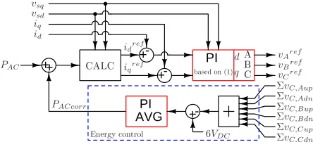
The MMC used as grid interface to klystron modulators requires the control of the AC active and reactive powers and the DC voltage, to recharge the capacitor bank before the next pulse. The proposed concept of the controller is presented in Fig. 3. The AC power references are used to compute the d, q current references for the PI phase current controllers [21] based on (1). The MMC has distributed energy storage, and the overall energy stored in the converter must be actively maintained. In [17] the energy stored in each phase is controlled by varying the circulating current reference and this approach is typical when the MMC is used as an inverter, e.g. drives. In the application analysed in this paper, the DC power is imposed by the load and the energy control loop can only act on the AC active power reference (Fig. 3). NamingPACcorr,
as the active power component used for energy control, the relation between the sum of all cell capacitor voltages vtot
(stored energy) andPACcorr is approximated by:
PACcorr=Ccell VDC
N dvtot
dt (7)
where N is the number of submodules per arm and VDC
Energy Control AC Power Control Phase Current Control Circulating Current Control ref q d i , ref C B A
v , ,
AC current reference AC voltage reference DC Voltage Control Phase Balancing ref Acirc i ref ADC v Circulating Current reference DC voltage reference Normalisation Arm Balancing
CAdnref Adn Aup C ref Aup v v v v , ,
Modulation and Cell Balancing Cell Capacitors
[image:3.612.73.280.56.281.2]Gate signals
Fig. 3. AC and DC side control strategies for the MMC supplying klystron modulators.
under the assumption that the cells within converter arms are well balanced and the average cell voltages of all arms are close to the nominal cell voltage VDC
N . A PI controller can
be designed to ensure thatvtotfollows the reference, equal to
6·VDC. The controller is an outer loop to the phase currents
controller, and its bandwidth has to be significantly lower. The AC side control diagram is shown in Fig. 4, where reactive power is set to zero for simplicity;AV Gindicates a periodical average filter with a period of 20msto remove voltage ripple; and signals entering PI controllers indicate errors if from comparison nodes, feed-forward terms otherwise.
The DC side control diagram is presented in Fig. 5, for phase A. The DC voltage controller generates the DC current reference which contributes to circulating current references (one third of the DC current). The controller is a slow PI acting on the average DC voltage, thus providing a constant DC cur-rent reference. Each circulating curcur-rent reference is corrected in order to provide phase and arm balancing. Similarly to [16] where the total phase energy is controlled, a PI controller can be set to ensure that the average of the sum of cell capacitors is the same in all three phases. Each phase balancing loop will output a DC offset for the circulating current reference.
PI + + -++ PI AVG +-PAC PACcorr CALC iq id
idref
iqref
vsd vsq d q A B C
vAref
vBref
vCref
6VDC
ΣvC,Aup ΣvC,Adn ΣvC,Bup ΣvC,Bdn ΣvC,Cup ΣvC,Cdn
basedon(1)
[image:3.612.325.549.59.227.2]Energyontrol
Fig. 4. AC side control diagram.
vC,Aup
vC,Adn
dn up jABC i ij C v ,, , , 3 1 DC V DC v ref A v
vC,Aup
vC,Adnref Acirc I ref Acirc I
Aup Adn
Acirc i i
i
[image:3.612.60.282.611.712.2]2 1 ref Acirc i ref ADC v ref Acirc i 50 PI AVG +-++ Phase Balancing +- PI 3 1 +++ CALC +-PI Based on (2) A i PI AVG +-Arm Balancing Feed-forward
Fig. 5. DC side control diagram - Phase A of the MMC.
Naming∆IAcircas the phase A circulating current correction,
the relation between the sum of the phase A cell capacitor voltages,vAtot, and the current correction is approximated by:
∆IAcirc= Ccell
N
dvAtot
dt (8)
The previous approximation is valid under the same assump-tions as the one of (7). The sum of the offset components is zero, guaranteeing that there is no DC offset in the DC current. The arm balancing controller requires a 50Hz component in the circulating current [7], [15], [18] which ensures zero average arm powers, enabling capacitor balancing. A pulsed DC load with a repetition rate of 50Hz is a source of imbalance for the arms and it will be discussed in the following sections.
The PI controller for DC current regulation, based on equation (2), tracks constant references with zero steady-state error. In this case the reference is not constant because of the 50Hz components. Also, the controller has to suppress the second harmonic current induced by capacitor ripple. If a high bandwidth controller is used, acceptable tracking errors are possible, as shown later in the simulation results. If perfect tracking is required, a proportional-resonant controller can be designed [22]. In any case, a DC voltage feed-forward is provided to attenuate the impact of the DC voltage ripple on the current control.
The modulation algorithm produces the gate signals for all the cells based on the arm references (5, 6). The modulation adopted in this paper is a level-shifted carrier-based algorithm with sorting of the cell capacitor voltages considering dynamic allocation of the carriers to the specific cells [1], [14], [23] also known as nearest level control with pulsed width modulation (NLC+PWM) [24]. In the given algorithm only one cell in an arm performs PWM at a time and the balancing of the cells is guaranteed by the sorting algorithm.
III. PULSEDLOADEFFECTS AND THENEED FORARM
BALANCING
currents of all the six converter arms are different, leading to different average arm powers and causing their imbalance. If arm balancing is not applied, i.e. if the circulating current reference is constant, the sum of all capacitor voltages of upper and lower arms (the overall available arm voltage) start diverging. This is illustrated for the case of an MMC rated at 20kVDC voltage and 16.6MW power, under pulsed load conditions, by showing the sum of all capacitor voltages of the phase A upper and lower arms together with the corresponding voltage references in Fig. 6. At 0.35s overmodulation occurs in the lower arm, causing low frequency distortion of the waveforms that leads to an increased AC power fluctuation, manifested with the low frequency region distortion [7], [10]. In order to analyse the imbalance, average upper and lower arm powers have to be computed. In ideal conditions, when the AC waveforms contain only the fundamental component, DC current is constant and the arm balancing is not applied, only the mean value, VDC, and the 50Hz component vDC50
of the DC voltage are relevant for power balance:
vDC=VDC+vDC50 (9)
The average upper arm power during one period of the fundamentalPAup=pAup is given by:
PAup=−vAup·iAup
=−VDC·IAcirc
2 −
vDC50·iA
4 +
vA·iA
2
(10)
where the products of a DC quantities and 50Hzquantities are neglected since they do not contribute to the average power. Note that due to the constant circulating current reference the DC side control variable was approximated as vADC = vADCref =vDC. If equal AC and DC powers are assumed,
i.e. PAC = 3·vA·iA =PDC =VDC·IDC, the upper and
lower arm powers become:
PAup =−
vDC50·iA
4 PAdn=
vDC50·iA
4 (11)
The previous equations imply that with non-zero 50Hz com-ponent in the DC voltage, there will be an imbalance between upper and lower converter arm average powers. This causes capacitor voltage drift, which will stop only when overmod-ulation is reached. The effect is present in all the phases but
0 10 20
Upper arm volt. [kV]
0 0.2 0.4 0.6 0.8 1
0 10 20
Lower arm volt. [kV]
Time [s]
[image:4.612.78.266.575.702.2]Available Reference
Fig. 6. Phase A upper (top) and lower (bottom) arm modulation signals and total cell capacitor voltages without arm balancing with the converter operating according to the ratings in Table II for the pulse position of
0.534rad.
varies depending on the phase shift between phase current and the DC voltage 50Hzripple.
The only way to balance the arm powers with the proposed control architecture and modulation strategy described by (5 and 6), is to act on the current references. To guarantee low AC power fluctuation, the AC reference should remain unchanged, and therefore the modification of the circulating current ref-erences is necessary. As previously discussed, the frequency components of the arm currents and voltages that contribute to the absorbed arm powers are dominated by DC and 50Hz, and therefore those are assumed to be added to the circulating current. A DC offset in the circulating current affects both arm powers in the same way and therefore it can be used as a tool to maintain the energy stored in the converter phase (phase balancing) [17]. Adding a 50Hzcomponent to the circulating current affects upper and lower arm powers in an opposite way, and therefore it can be used for the purpose of arm balancing [7], [15], [18]. In this case, the circulating current modification is based on average energy/power evaluation. Assuming that the circulating current has a generic 50Hz component, used for arm balancing, it can be represented for phase A as:
iAcirc=IAcirc+iAcirc50 (12)
whereIAcirc is the DC component andiAcirc50 is the 50Hz
component of phase A circulating current reference. In this case, based on (2), the vADCref can not longer be
approxi-mated with vDC, but must be written as:
vADCref =vDC+ 2Larm· d
dtiAcirc50 (13)
Average upper and lower arm powers are described by:
PAup=−vDC50
·iAcirc50
2 −
vDC50·iA
4
−Larm· d
dtiAcirc50· iA
2 +vA·iAcirc50
(14)
and
PAdn=−
vDC50·iAcirc50
2 +
vDC50·iA
4
+Larm· d
dtiAcirc50· iA
2 −vA·iAcirc50
(15)
From the equations, the only way both upper and lower arm powers can be equal to zero at the same time, is if:
vDC50·iAcirc50
2 = 0 (16)
Equation (16) is true only if the 50Hz DC voltage ripple and the 50Hz circulating current reference are phase shifted by π2. In that case, based on the amplitudes and phase angle of all variables from (14, 15) the amplitude of the 50 Hz component of the circulating current (IAcirc50, for phase A)
TABLE I
AMPLITUDE AND PHASE ANGLE OF50HzCOMPONENTS.
Signal Amplitude label Phase label
iA Im φAi
vA Vm φAv
vDC50 VDC50 φDC50
iAcirc50 IAcirc50 φAcirc50
When the phase angle of the circulating current is fixed to
φAcirc50=φDC50−π2, the amplitude of the 50Hzcomponent
of the circulating current reference is:
IAcirc50= N U MDENAA
= VDC50
·Imcos(φDC50−φAi)
4
Vmcos(φDC50−π2−φAv)−LarmωIm
cos(φDC50−φAi)
2
(17)
where ω is the grid frequency. As shown in Fig. 7 for phase A, an arm balancing controller can be designed for each of the three phases to provide the 50Hz component of the circulating current reference in order to compensate for the arm imbalance induced by the pulsed DC load. The amplitude and phase of the 50Hzcurrent reference component are provided as feed-forward terms, calculated using (17) and knowing the operating point of the converter. A correction to the amplitude is provided by a PI controller which ensures equal energy stored in the upper and lower arms in each phase. The difference between upper and lower arm average powers
∆PAarm, based on (14) and (15), is described by:
∆PAarm(t) =
Ccell·VDC N
d∆vAarm(t)
dt (18)
where∆vAarm is the difference between the sums of upper
and lower arm cell capacitor voltages and should be controlled to zero for arm balancing. To provide the difference in power needed for arm balancing, a corresponding amplitude of the 50Hzcurrent IAcirc50 is given by:
IAcirc50=
Ccell·VDC N·DENA
· d∆vAarm
dt (19)
Using (19) as the control plant, a PI controller can be designed to add a closed loop correction term toN U MAand
ensure that the two arms store an equal amount of energy. From (17), the circulating current amplitudes in the different
CALC
PI S/H 20ms
+-AVG 20ms
++
A
i
A
v 50
DC
v
0
Aarm
V
X /
A
NUM
A
DEN
Aarm
P
50
Acirc
CALC
50
Acirc
I iAcirc50ref
DC cell
A
V C s
DEN N
Adn C Aup C Aarm
v v
v
[image:5.612.54.296.595.720.2], ,
Fig. 7. Proposed arm balancing controller.
phases depend on the phase shift between the 50HzDC link voltage ripple and the corresponding AC voltages and currents. Considering this, a net amount of 50Hz component will be generally present in the total DC current, even if the DC current reference from the DC voltage controller is constant. This will increase the DC power fluctuation, but the AC power fluctuation will be maintained at a low level.
A similar balancing algorithm with a 50Hz circulating current component aligned with the AC voltage reference of each phase is suggested in [18], where only a proportional controller is used to cope with transient arm imbalances. In [15] a PI based arm balancing method with a 50Hzcomponent in the circulating current suggested that either arm balancing can be provided by controlling the amplitude when the angle of the current is fixed or by controlling the angle when the amplitude is fixed. Furthermore, it has been suggested that the arm balancing with the lowest current amplitudes is provided if the 50Hzcirculating current is aligned with the grid voltage of the corresponding phase.
In the method proposed in this paper, the same phase angle (π2rad) is used for all circulating currents and it is defined by the DC voltage ripple phase. This method does not guarantee minimum amplitude of the 50Hzbalancing current, but enables an arm balancing control that is decoupled from the phase energy controller. In fact, forcing (16) in (14, 15) means that a change in the 50Hzbalancing current does not affect the total phase power.
IV. SIMULATIONRESULTS
Simulation results from a PLECS model of the converter are proposed to validate the overall controller and the proposed arm balancing method on an MMC rated for 20kV DC and 16.6MW. The converter and load parameters used in the simulation are given in Table II. The converter passives are sized according to [25]. The load is emulated with an ideal rectangular pulse current source with given amplitude, duration and repetition rate. The bandwidth and phase margin (PM) of the controllers used in the simulation model are presented in Table III.
Based on (17),DEN and the amount of 50Hzcirculating currents can be computed for a given 50HzDC voltage ripple. As shown in Fig. 8, the denominators of all three phases have two zero crossings and in those positions the computation of the circulating current amplitude is not possible, meaning that the arm balancing control cannot be implemented with the
−3 −2 −1 0 1 2 3
−10 −5 0 5 10
φDC50[rad]
Denominator amplitude [kV]
[image:5.612.335.545.625.715.2]phase A phase B phase C
Fig. 8. The denominator values vs. the 50HzDC voltage ripple phase
TABLE II
CONVERTER AND LOAD PARAMETERS USED IN THE SIMULATION MODEL AND EXPERIMENTAL RIG.
Description Simulation Experiments Rated power 16.6MW 7kW
DC voltage 20kV 400V
AC voltage 10.5kV 225V
Number of cells per arm 20 4 Nominal cell voltage 1kV 100V
Phase inductance 3.5mH 3mH
Arm inductance 1.8mH 1.5mH
Cell capacitance 13.8mF 3.3mF
DC link capacitance 8.3mH 8.5mF
DC voltage droop 2kV 40V
Pulse frequency 50Hz 50Hz
Pulse duration 140µs ≈150µs
Peak pulse current 118.57kA 3.3kA
TABLE III
CONTROLLER GAINS USED IN SIMULATION AND EXPERIMENTAL IMPLEMENTATION.
Controller Simulation Experiments Bandwidth PM Bandwidth PM Phase Current 2000rad/s 87◦ 2670rad/s 86◦ Circ. Current 3750rad/s 89◦ 5000rad/s 89.4◦
Energy 10rad/s 87◦ 8.8rad/s 71◦ DC voltage 12.7rad/s 52◦ 14.2rad/s 86◦ Ph. balancing 20rad/s 88◦ 120rad/s 89.9◦ Arm balancing 8rad/s 38◦ 10.5rad/s 87.3◦
proposed approach. The phase angle of the DC link voltage ripple depends on the position of the load pulse with respect to the phase A grid voltage positive gradient zero crossing. Assuming the converter phases are symmetric, it is enough to analyse the pulse positions between grid voltage phase A and phase B zero crossings (i.e. from 0 to 2·3πrad). The converter has been simulated for 21 equally spaced pulse positions. Amplitude and duration of the pulse are constant.
Fig. 9 presents the AC and DC power fluctuations as a function of pulse position. In two out of 21 observed pulse positions, balancing is not possible because one of denomina-tors is close to zero. In those positions, AC power fluctuation is beyond 2%specification. In the other19pulse positions, the achieved AC power fluctuation is about 0.2%even in the cases when the DC power fluctuation is 80%. It is worth mentioning that DC power fluctuation increases when approaching the zero crossings of one of the DEN, because the amplitude of the 50Hz circulating current needed for balancing increases rapidly.
The amplitudes of the three circulating current references in the different pulse positions are presented in Fig. 10. The first critical point (pulse position of 0.105rad close to grid voltage phase A zero crossing) corresponds to the DENA
zero crossing, while the second critical position (1.152rad) corresponds to theDENC zero crossing.
From the theoretical analysis and from simulation results
0 0.5 1 1.5 2
0.15 0.2 0.25
AC power fluctuation [%]
Pulse position [rad]
0 0.5 1 1.5 2
10 20 30 40 50 60 70 80
DC power fluctuation [%]
[image:6.612.316.556.59.278.2]Pulse position [rad]
Fig. 9. AC and DC power fluctuation for different pulse positions.
0 0.5 1 1.5 2
−200 −100 0 100 200 300
Circ. curr. 50Hz amplitude [A]
Pulse position [rad] phase A
[image:6.612.67.283.314.412.2]phase B phase C
Fig. 10. Amplitudes of the 50Hzcirculating currents for different pulse
positions.
it can be seen that the sum of the three 50Hz circulating current components will generally result in a non-zero DC current ripple at 50Hz, with an amplitude dependent on the pulse position.
Based on (17), the expression for the resulting 50Hz DC current ripple component can be found as a function of the DC voltage ripple angle and amplitude. Knowing the expression for the DC current, the load current (50Hz component) and the DC link capacitance, the DC voltage ripple amplitude can be computed for an arbitrary DC voltage angle. In addition, the voltage ripple phase angle is π2radshifted from the load and DC current, and if ideal pulse is assumed, the relation between pulse position in radians and the DC voltage ripple 50Hzcomponent angle can be derived:
φDC50=π−P P −ω
Tpulse
2 (20)
whereP P stands for pulse position in radians andTpulse for
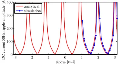
pulse duration. The obtained amplitude of the DC current rip-ple using the analytical model and by simulation is presented in Fig. 11.
In the considered application, the pulse can be synchronised to the grid voltages and therefore a pulse position where all the denominators are far from their zero crossings can be
−3 −2 −1 0 1 2 3
0 100 200 300 400
φDC50[rad]
DC current 50Hz ripple amplitude [A]
[image:6.612.334.530.620.726.2]analytical simulation
selected. The following simulation results relate to a fixed pulse position of 0.534rad. Fig. 12 presents the AC and DC side currents and voltages. The obtained AC currents are sinusoidal with a THD of 0.19%. The selected pulse position corresponds to a relatively low 50Hz component in the DC current ripple (0.6%). In the AC converter phase voltages (vconAin Fig. 1) there are no visible signs of distortion since
the overmodulation is not present. The DC voltage has a 2kV
voltage droop occurring approximately 1.7ms after phase A current zero crossing. The obtained AC power fluctuation is 0.22% while the obtained DC power fluctuation is 12.1%.
Fig. 13 shows the action of the arm balancing controller on the 50Hzcirculating current references. Fig. 14 presents phase A upper and lower arm reference and available voltage (the sum of all cell capacitor voltages of an arm). Arm balancing is successful and the reference voltage is always lower than the available arm voltage, avoiding the overmodulation that was present in Fig. 6.
Fig. 15 (top) shows the energy controller dynamics, by observing the average sum of all cell capacitor voltages in two cases, when arm balancing is applied and when it is not. Att= 1.5 sthe load peak current is reduced by 20%and the energy controller dynamics are not affected by the presence
−1000 0 1000
Currents [A]
Phase A Phase B Phase C
800 850
DC current [A]
−10 0 10
Voltages [kV]
Phase A Phase B Phase C
1.8 1.81 1.82 1.83 1.84 1.85 19
20 21
DC voltage [kV]
[image:7.612.336.533.59.193.2]Time [s]
Fig. 12. From top to bottom: Phase currents, DC currents, Phase
voltages and DC voltage.
−50 0 50
Circulating current
50Hz ref. [A]
Phase A Phase B Phase C
1.8 1.81 1.82 1.83 1.84 1.85 200
300 400
Phase A circ. current [A]
Time [s]
[image:7.612.332.529.261.385.2]Reference Actual
Fig. 13. Phase A, B and C 50Hzcirculating current references
gener-ated by the arm balancing controller (top plot) and phase A circulating current and its reference (bottom plot).
0 10 20
Upper arm volt. [kV]
0 0.2 0.4 0.6 0.8 1
0 10 20
Lower arm volt. [kV]
Time [s]
Available Reference
Fig. 14. Phase A upper (top) and lower (bottom) arm modulation signals and total cell capacitor voltages with arm balancing with the converter operating according to the ratings in Table II for the pulse position of
0.534rad.
120 130 140 150
Average sum [kV]
No arm balancing Arm balancing
0 0.5 1 1.5 2 2.5 3
−100 −50 0 50
Circ. cur. amplitude [A]
Time [s]
Ph. A Ph. B Ph. C
Fig. 15. The average of the sum of all cell capacitor voltages (top) and amplitude of the circulating currents used for arm balancing (bottom) during load power transient.
of the arm balancing controller whose dynamics are presented in the bottom of Fig. 15.
V. EXPERIMENTAL RESULTS
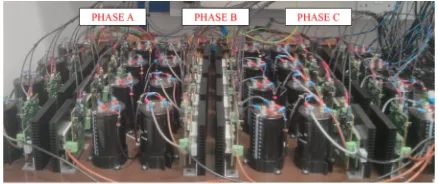
A small scale prototype has been built to validate the behaviour of the grid connected MMC under pulsed DC load conditions with the proposed arm balancing controller. A 4 cell per arm, 7kW converter has been designed by scaling both voltages and currents with the same scaling factor. A picture of the experimental converter is shown in Fig. 16. A thyristor controlled resonant circuit has been designed to emulate the pulsed DC load, which generates a 3.3kA current pulse in a shape of half a sinusoid (Fig. 17). Table II lists the converter and the load parameters. The resonant load parameters are designed to provide the same average current (16.5A) as the ideal rectangular pulse. Table III lists the bandwidth and PM of all controlled used in the experimental implementation.
[image:7.612.71.269.359.554.2] [image:7.612.65.272.603.706.2]Fig. 16. Three phase MMC with 4 cells per arm.
MMC
CDC Cload, RC Rload
Lload, RL Qload
iload IDC
[image:8.612.319.559.58.159.2]vDC vout
Fig. 17. Resonant load circuit.
350 400 450
DC voltage [V]
−0.8 −0.6 −0.4 −0.2 0 0.2 0.4 0.6 0.8 0
1 2 3
Load current [kA]
Time [ms]
Fig. 18. DC voltage and load current during the pulse.
This is due to the non fully symmetrical converter arms and to the errors in the acquisition system. Therefore some arm balancing is necessary even with no-load or resistive DC load conditions.
Experimental results consider the same pulse position range discussed in simulation. Fig. 19 presents the AC and DC power fluctuation measured through the HPI on the experimental prototype for various pulse positions. The AC power fluctua-tion is not significantly affected by the pulse posifluctua-tion, being always between 1.4 and 1.7%, while the DC power fluctuation increases with the increase of the DC current ripple in a similar way as in simulation results. Here the critical regions are extended only beacuse the maximum circulating current 50Hzcomponent amplitude is limited to 3Ain order to avoid tripping the converter due to the high arm currents. Fig. 20 presents obtained amplitudes of the circulating current 50Hz
component references captured though the HPI for various pulse positions. The obtained dependence is in agreement with the one seen in simulation.
The converter phase currents measured with the oscilloscope in steady state conditions for the pulse position of 0.534rad
are presented in Fig. 21. The currents are well balanced with the low harmonic spectrum not exceeding 0.4% of the fundamental and the THD of approximately 2%.
Captured converter AC and DC side waveforms under
0 0.5 1 1.5 2
1.46 1.48 1.5 1.52 1.54 1.56 1.58 1.6
AC power fluctuation [%]
Pulse position [rad]
0 0.5 1 1.5 2
10 15 20 25 30 35 40
DC power fluctuation [%]
[image:8.612.82.265.193.248.2]Pulse position [rad]
Fig. 19. AC and DC power fluctuation for different pulse positions
obtained by experiment.
0 0.5 1 1.5 2
−3 −2 −1 0 1 2 3
Circ. curr. 50Hz amplitude [A]
[image:8.612.338.529.205.308.2]Pulse position [rad] phase A phase B phase C
Fig. 20. Amplitudes of the circulating currents for different pulse posi-tions obtained experimentally.
0 0.01 0.02 0.03 0.04 −30
−20 −10 0 10 20 30
Phase currents [A]
Time [s]
Phase A Phase B Phase C
Fig. 21. Converter/grid phase currents under steady-state conditions.
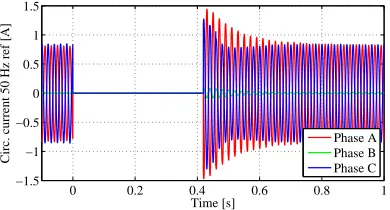
steady state conditions for the position of 0.534radare shown in Fig. 22. The droop in the DC voltage occurs approximately 1.7ms after phase A current zero crossing. The amplitude of 50Hzcomponent in the DC current ripple is similar as in the case of simulation - 0.6%of the nominal DC current. Fig. 23 presents the sum of cell capacitor voltages of upper and lower arms obtained through the HPI. Initially the arms are perfectly balanced and the arm balancing controllers are operational. At
t= 0 sthe arm balancing controllers are disabled and the cell
capacitor voltages of the upper and lower arms start diverging. Att= 0.4 sthe arm balancing controllers are re-enabled, and the sum of capacitor voltages of the upper and lower arms start converging. The selected pulse position has a more significant effect to phases A and C, while they almost do not cause any imbalance in phase B.
The circulating current 50Hz component references ob-tained through the HPI corresponding to the transient are presented in Fig. 24. For this pulse position, in the steady state, the sum of the three references is close to zero.
VI. CONCLUSION
[image:8.612.72.268.299.416.2] [image:8.612.330.534.353.442.2]−20 0 20
Ph. A current [A]
−200 0 200
Ph. A voltage [V]
10 15 20
DC current [A]
0 0.01 0.02 0.03 0.04 350
400 450
DC voltage [V]
Time [s]
Fig. 22. From top to bottom: Phase A current, DC current, phase A voltage and DC voltage.
350 400 450
Ph. A sum [V]
∆vC,Aup
∆vC,Adn
350 400 450
Ph. B sum [V]
∆vC,Bup
∆vC,Bdn
0 0.2 0.4 0.6 0.8 1
350 400 450
Ph. C sum [V]
Time [s]
∆vC,Cup
∆vC,Cdn
Fig. 23. Sum of the phase upper arm and lower arm cell capacitor voltages under steady state conditions, when arm balancing controller is disabled and re-enabled.
0 0.2 0.4 0.6 0.8 1
−1.5 −1 −0.5 0 0.5 1 1.5
Circ. current 50 Hz ref [A]
Time [s]
[image:9.612.70.269.57.262.2]Phase A Phase B Phase C
Fig. 24. Circulating current reference 50Hzcomponent used for arm
balancing under steady state conditions, when arm balancing controller is disabled and re-enabled.
pulsed load is representative of the klystron modulators used in the next generation linear particles accelerator under study at CERN. The MMC has been selected for its decoupled AC and DC control capability, allowing the suppression of the DC power fluctuation from the AC side.
The repetition rate of the pulsed load is 50Hz, causing imbalance of the cell capacitor voltages between upper and lower arms in each phase. Without suitable provisions, over-modulation occurs in one arm of each phase, leading to distorted AC waveforms and large AC power fluctuation. The proposed arm balancing method is based on the addition of 50Hz components in the circulating current references, orthogonal to the 50HzDC voltage ripple. Detailed analysis of the proposed method has been developed and the balancing controller has been design accordingly. The proposed method is sensitive to pulse position, and balancing is not possible for 6 pulse positions within the grid voltage period. However, if the klystron modulators are synchronised with the grid, the pulse position within the grid period can be controlled, avoiding the critical regions.
Simulation results provide a first validation of the behaviour predicted by the analytical model. In addition, the proposed controller has been validated on a 400VDC/7kW experimen-tal prototype. The obtained AC power fluctuation for pulse positions outside the critical regions is approximately 1.6%. The success of the arm balancing method is proven and the required circulating current references are in agreement to those obtained by simulation.
REFERENCES
[1] M. Saeedifard and R. Iravani, “Dynamic performance of a modular multilevel back-to-back HVDC system,”IEEE Transactions on Power Delivery, vol. 25, no. 4, pp. 2903–2912, Oct. 2010.
[2] R. Marquardt, “A new modular voltage source inverter topology,” in European Power Electronics Conference (EPE), Sep. 2003.
[3] M. Jankovic, A. Watson, J. Clare, P. Wheeler, and D. Aguglia, “Optimal power system and grid interface design considerations for the CLICs klystron modulators,” in2014 IEEE International Power Modulator and High Voltage Conference (IPMHVC), pp. 83–88, Jun. 2014.
[4] D. Aguglia and E. Sklavounou, “Klystron modulators capacitor chargers design compromises for ac power quality increase of the compact linear collider (CLIC),” in International Symposium on Power Electronics Power Electronics, Electrical Drives, Automation and Motion, pp. 1535– 1541, Jun. 2012.
[5] D. Dannheim, P. Lebrun, L. Linssen, D. Schulte, and S. Stapnes, “Clic e+e- linear collider studies - input to the snowmass process 2013,” in Snowmass on the Mississippi CSS, Aug. 2013.
[6] F. C. Magallanes, D. Aguglia, P. Viarouge, C. de Almeida Martins, and J. Cros, “A novel active bouncer system for klystron modulators with constant ac power consumption,” in2013 19th IEEE Pulsed Power Conference (PPC), pp. 1–6, Jun. 2013.
[7] M. Jankovic, A. Costabeber, A. Watson, and J. Clare, “Control of a grid connected modular multilevel converter under pulsed dc load,” inIECON 2015 - 41st Annual Conference of the IEEE Industrial Electronics Society, pp. 002 526–002 531, Nov. 2015.
[8] S. Norrga, L. ¨Angquist, K. Ilves, L. Harnefors, and H. P. Nee, “Decou-pled steady-state model of the modular multilevel converter with half-bridge cells,” in6th IET International Conference on Power Electronics, Machines and Drives (PEMD 2012), pp. 1–6, Mar. 2012.
[9] M. A. P´erez, R. L. F., and J. Rodr´ıguez, “Decoupled current control of modular multilevel converter for HVDC applications,” in2012 IEEE International Symposium on Industrial Electronics, pp. 1979–1984, May. 2012.
[10] A. Lachichi and L. Harnefors, “Comparative analysis of control strate-gies for modular multilevel converters,” in2011 IEEE Ninth Interna-tional Conference on Power Electronics and Drive Systems, pp. 538– 542, Dec. 2011.
[image:9.612.72.268.313.474.2] [image:9.612.72.267.533.638.2][12] W. van der Merwe, P. Hokayem, and L. Stepanova, “Analysis of then
-cell single phase mmc natural balancing mechanism,”IEEE Journal of Emerging and Selected Topics in Power Electronics, vol. 2, no. 4, pp. 1149–1158, Dec. 2014.
[13] A. Hassanpoor, L. ¨Angquist, S. Norrga, K. Ilves, and H. P. Nee, “Tolerance band modulation methods for modular multilevel converters,” IEEE Transactions on Power Electronics, vol. 30, no. 1, pp. 311–326, Jan. 2015.
[14] M. A. Perez, S. Bernet, J. Rodriguez, S. Kouro, and R. Lizana, “Circuit topologies, modeling, control schemes, and applications of modular multilevel converters,”IEEE Transactions on Power Electronics, vol. 30, no. 1, pp. 4–17, Jan. 2015.
[15] S. Fan, K. Zhang, J. Xiong, and Y. Xue, “An improved control system for modular multilevel converters with new modulation strategy and voltage balancing control,”IEEE Transactions on Power Electronics, vol. 30, no. 1, pp. 358–371, Jan. 2015.
[16] M. Hagiwara, R. Maeda, and H. Akagi, “Control and analysis of the modular multilevel cascade converter based on double-star chopper-cells (MMCC-DSCC),” IEEE Transactions on Power Electronics, vol. 26, no. 6, pp. 1649–1658, Jun. 2011.
[17] M. Hagiwara and H. Akagi, “Control and experiment of pulsewidth-modulated modular multilevel converters,”IEEE Transactions on Power Electronics, vol. 24, no. 7, pp. 1737–1746, Jul. 2009.
[18] J. Pou, S. Ceballos, G. Konstantinou, V. G. Agelidis, R. Picas, and J. Zaragoza, “Circulating current injection methods based on instanta-neous information for the modular multilevel converter,”IEEE Transac-tions on Industrial Electronics, vol. 62, no. 2, pp. 777–788, Feb. 2015. [19] M. Jankovic, A. Watson, A. Costabeber, and J. Clare, “Control of a modular multilevel converter with pulsed dc load,” in2016 IEEE Energy Conversion Congress and Exposition (ECCE), pp. 1–8, Sep. 2016. [20] W. Yang, Q. Song, and W. Liu, “Decoupled control of modular multilevel
converter based on intermediate controllable voltages,”IEEE Transac-tions on Industrial Electronics, vol. 63, no. 8, pp. 4695–4706, Aug. 2016.
[21] A. Yazdani and R. Iravani, Grid-Imposed Frequency VSC System: Control in dq-Frame, pp. 541–. Wiley-IEEE Press, 2010. [Online]. Available: http://ieeexplore.ieee.org/xpl/articleDetails. jsp?arnumber=6739414
[22] R. Teodorescu, F. Blaabjerg, M. Liserre, and P. C. Loh, “Proportional-resonant controllers and filters for grid-connected voltage-source con-verters,”IEE Proceedings - Electric Power Applications, vol. 153, no. 5, pp. 750–762, Sep. 2006.
[23] E. K. Amankwah, J. C. Clare, P. W. Wheeler, and A. J. Watson, “Multi carrier PWM of the modular multilevel vsc for medium voltage applications,” in 2012 Twenty-Seventh Annual IEEE Applied Power Electronics Conference and Exposition (APEC), pp. 2398–2406, Feb. 2012.
[24] M. Rejas, L. Mathe, P. D. Burlacu, H. Pereira, A. Sangwongwanich, M. Bongiorno, and R. Teodorescu, “Performance comparison of phase shifted PWM and sorting method for modular multilevel converters,” in 2015 17th European Conference on Power Electronics and Applications (EPE’15 ECCE-Europe), pp. 1–10, Sep. 2015.
[25] M. Zygmanowski, B. Grzesik, and R. Nalepa, “Capacitance and in-ductance selection of the modular multilevel converter,” in2013 15th European Conference on Power Electronics and Applications (EPE), pp. 1–10, Sep. 2013.
Marija Jankovic(S’10-M’17) was born in Val-jevo, Serbia in 1988. She received the B.Sc. and M.Sc. in electrical engineering and computer science at the University of Belgrade, Serbia in 2010 and 2011, respectively; and the Ph.D. degree in electrical and electronic engineering at the University of Nottingham, UK in 2017.
From 2016 she has been working as a Re-search Fellow with the Power Electronics, Ma-chines and Control Group, at the University of Nottingham. Her research interests include high power multilevel topologies, converter modelling and control.
Alessandro Costabeber (S’09-M’13)
received the Degree with honours in
Electronic Engineering from the University
of Padova, Padova, Italy, in 2008 and the Ph.D. in Information Engineering from the same university in 2012, on energy efficient architectures and control techniques for the development of future residential microgrids.
In the same year he started a two-year research fellowship with the same university. In 2014 he joined the PEMC group, Department of Electrical and Electronic Engineering, University of Nottingham, Nottingham, UK as Lecturer in Power Electronics. His current research interests include HVDC converters topologies, high power density converters for aerospace applications, control solutions and stability analysis of AC and DC microgrids, control and modelling of power converters, power electronics and control for distributed and renewable energy sources.
Dr. Costabeber received the IEEE Joseph John Suozzi INTELEC Fellowship Award in Power Electronics in 2011.
Alan Watson (S’03-M’08) received his MEng (Hons) degree in Electronic Engineering from the University of Nottingham in 2004 before pursuing a PhD in Power Electronics, also at Nottingham.
In 2008, he became a Research Fellow in the Power Electronics Machines and Control
Group, working on the UNIFLEX project
(http://www.eee.nott.ac.uk/uniflex/). Since
2008, he has worked on several projects in the area of high power electronics including high power resonant converters, high voltage power supplies, and multilevel converters for grid connected applications such as HVDC and FACTS. In 2012 he was promoted to Senior Research Fellow before becoming a Lecturer in High Power Electronics in 2013. His research interests include the development and control of advanced high power conversion topologies for industrial applications, future energy networks, and VSC-HVDC.
Jon C. Clare(M’90-SM’04) was born in Bristol, U.K., in 1957. He received the B.Sc. and Ph.D. degrees in electrical engineering from the University of Bristol, Bristol.
From 1984 to 1990, he was a Research Assistant and Lecturer with the University of Bristol, where he was involved in teaching and research on power electronic systems. Since 1990, he has been with the Power
Electronics, Machines and Control Group,