http://wrap.warwick.ac.uk/
Original citation:
Rochford, L. A. (Luke A.), Keeble, Dean Samuel, Holmes, O. J., Clarkson, Guy J. and
Jones, T. S. (Tim S.). (2014) Controlling templating effects at the organic/inorganic
interface using (111) oriented copper iodide. Journal of Materials Chemistry C, Volume 2
(Number 30). pp. 6056-6060.
Permanent WRAP url:
http://wrap.warwick.ac.uk/66520
Copyright and reuse:
The Warwick Research Archive Portal (WRAP) makes this work of researchers of the
University of Warwick available open access under the following conditions.
This article is made available under the Creative Commons Attribution- 3.0 Unported
(CC BY 3.0) license and may be reused according to the conditions of the license. For
more details see
http://creativecommons.org/licenses/by/3.0/
A note on versions:
The version presented in WRAP is the published version, or, version of record, and may
be cited as it appears here.
Controlling templating e
ff
ects at the organic/
inorganic interface using (111) oriented copper
iodide
†
L. A. Rochford,*aD. S. Keeble,bO. J. Holmes,aG. J. Clarksonaand T. S. Jonesa
Structural templating of organic semiconductors affords control of out-of-plane film structure and molecular orientation with respect to solid surfaces. Herein we use a prototypical copper iodide (CuI)/ planar phthalocyanine system to produce detailed surface and crystal structure information using atomic force microscopy (AFM) and X-ray diffraction (XRD). The out-of-plane structure of the CuI layer was characterised and identified as the (111) plane of single crystal CuI. The dependance of surface morphology and grain size in the CuI (111) templating layer upon substrate temperature was demonstrated. The formation of a thin film of iron phthalocyanine (FePc) on this model layer was characterised at multiple points during growth, changes in the surface morphology were observed, and the crystal structure of thefinalfilm was used to infer the molecular orientation therein. These changes were elucidated using the re-determined single crystal structure of FePc which is also presented.
Introduction
The ability to control the morphology and crystal structure of organic semiconductors allows their physical and electronic properties to be tuned concomitantly.1–3Desirable characteris-tics for specic device applications including organic photo-voltaic (OPV), thin lm transistor (OTFT) and light emitting diode (OLED) geometries can be preferentially selected.4,5 To
this end, thin organic6or inorganic7layers have been employed
as structural templates for the improvement of device parame-ters. A prominent example of this methodology is the insertion of a copper(I) iodide interlayer between a transparent electrode (indium tin oxide) and a planar phthalocyanine (Pc) active layer to modify molecular orientation in the organiclm.7
The effect of this structural modication has been observed in OPVs8and theoretical simulations have been used to model the change in charge transport characteristics in phthalocya-nine/fullerene devices.9Despite this, the nature of the interac-tion causing this modication has not been studied in any depth. Planar Pc molecules are widely used in organic elec-tronics and have been used to fabricate a variety of efficient devices.10
The crystal structure of planar Pcs is inherently anisotropic due to face-to-face packing motifs creating short intermolecular distances within stacks and larger inter-stack spacings.11,12This
has been shown to impact charge transport in single crystals13
and thin lms.14 Therefore, controlling the direction along which the molecules have closest contacts can lead to improved device characteristics.15
We report the preparation and characterisation of evapo-rated copper iodide (CuI) thin lms at both ambient and elevated substrate temperatures. Grain size and morphology in theselms was shown to be strongly dependant on substrate temperature during growth and the use of high growth temperaturelms as structural templates for a planar phtha-locyanine (FePc) was explored. Control of both molecular orientation and grain size in FePclms was demonstrated using this methodology. The crystal structure of FePc was also re-determined to enable accurate assignment of the crystal struc-ture to the thinlms.
Results and discussion
Firstly, in order to fully understand the proposed organic molecule templating process, the crystal structure of the CuI layer prepared at ambient substrate temperatures, as previously shown in the literature, was determined. Evaporated CuIlms of 1 nm thickness, as used by Randet al.,9were prepared and
XRD patterns were recorded in which no CuI peaks were observed. Thickerlms (15 nm) were grown at the same rate (0.5 ˚
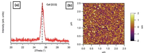
A s1), which produced a single broad (as shown in Fig. 1(a)) peak at 2q¼25.5corresponding to the (111) lattice spacing of CuI (ICSD no. 23 990). Atomic force microscopy (AFM) was used
a
Department of Chemistry, University of Warwick, Gibbet Hill Road, Coventry, CV4 7AL, UK. E-mail: [email protected]
bDepartment of Physics, University of Warwick, Gibbet Hill Road, Coventry, CV4 7AL,
UK
†Electronic supplementary information (ESI) available: Additional XRD traces of untemplated FePclms, a plot of surface roughnessvs.FePc thickness, expanded views of a high-angle CuI XRD trace and additional single crystal structure information are included. CCDC 996880. For ESI and crystallographic data in CIF or other electronic format DOI: 10.1039/c4tc00759j
Cite this:J. Mater. Chem. C, 2014,2, 6056
Received 15th April 2014 Accepted 10th June 2014
DOI: 10.1039/c4tc00759j
www.rsc.org/MaterialsC
Materials Chemistry C
PAPER
Open Access Article. Published on 13 June 2014. Downloaded on 11/03/2015 13:47:45.
This article is licensed under a
Creative Commons Attribution 3.0 Unported Licence.
View Article Online
to observe the morphology of the lm, which showed high polycrystallinity (Fig. 1). Thelms were made up of grains less than 20 nm in size and exhibited low surface roughness (Rq) values (0.7 nm), suggesting that CuI grows as a highly poly-crystallinelm with predominantly (111) out-of-plane orienta-tion at room temperature on SiO2.
If the (111) faces present in a highly polycrystalline CuI thin lm are responsible for the templating effect,19increasing the
size of these faces should allow observation of the nucleation process of an organic layer grown on top. To produce thinlms with larger grains more suitable for scanning probe imaging, the substrate temperature was increased to 200 C. This produced a clear change in morphology; 15 nm lms now consisted of dispersed islands with up to 80 nm high out-of-plane protrusions and roughly hexagonal shapes in AFM images (Fig. 2(a)). The growth was clearly in the form of a Volmer– Weber20(island growth) mode as islands with a variety of sizes
and heights were evident. This suggests both that islands are preferentially grown over layer-by-layer formation (no wetting layer was observed), and that islands have nucleated at various points during the growth process.21A three dimensional render
of the same image is also presented, showing clear faceting and steps in the islands of CuI which suggest that these features are single crystals (Fig. 2(b)).
XRD patterns of the island-like lms again showed only (111)-type reections, indicating that the orientation of the islands is unaltered by the change in growth conditions (a digitally magnied trace showing the (222) and (333) is shown in the ESI, Fig. SI03†). Furthermore, the hexagonal habit of the islands suggests 3- or 6-fold planar symmetry, and this is also consistent with the assignment of (111) oriented islands. Additionally, the decreased peak width, and observation of higher angle (111)-type reections such as the (222) and (333) from the island-likelm are both consistent with the assertion from AFM that the islands were mono-crystalline.
The elevated substrate temperature produced highly crys-talline CuI islands aligned with their (111) planes parallel to the substrate. This creates a non-uniform surface upon which to grow the organic overlayer, as molecules from the incident molecular beam will impinge on single-crystal CuI islands, as well as the areas of bare SiO2substrate between them. As the interaction between the CuI and FePc molecules was the focus of this study a complete coverage of the oriented CuI crystallites was required: to this endlms of 45 nm thickness were grown at
the same rate and elevated substrate temperature to produce a continuouslm with large (111) grains. This process produced highly crystalline continuous (111) orientedlms with grains up to 1mm (observed by AFM, Fig. 2(d)). In the corresponding XRD patterns (Fig. 2(e)) Laue fringes were observed around the (111) peak, conrming the high crystallinity and uniform thickness of thelm.
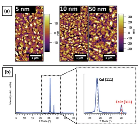
By creating (111) oriented CuIlms, uniform surfaces were provided upon which to observe the formation of FePc crystal-lites on the crystal faces responsible for the templating effect. Successive growth of FePc on to CuI (111)lms was carried out in situ without exposure to air to ensure no surface contami-nation was introduced. FePclms of 5, 10 and 50 nm thickness were grown aer cooling the CuIlms to room temperature in vacuum. The thinnest lms showed non-uniform nucleation and growth of FePc over the CuI (111) faces, and FePc islands were present in combination with areas of bare CuI substrate (Fig. 3(a)). This is in direct contrast to the behaviour usually observed with ambient substrate temperature growth of planar phtalocyanines on weakly interacting substrates such as glass or SiO2.22
In thickerlms (10 nm FePc) the number and size of the FePc grains increased, although CuI grain boundaries were still visible due to non-uniform coverage of the overlayer. In 50 nm FePclms large grains (up to 1 mm longest dimension) were observed and the CuI substrate is no longer visible. The grains were discrete and did not grow into one another as a continuous lm, suggesting that they were contained on the individual CuI (111) faces. Depositing FePc in this way increased the surface roughness of the system: the 5 nm FePc/CuI bilayer had anRqof 10.2 nm compared with 2.9 nm for the bare CuI. Increasing the thickness to 10 nm increased the roughness further (Rq¼15.5 nm) and at 50 nm theRqreached a peak of 17.4 nm.
These observations suggest that the FePc layer was also formedvia a 3D island growth mode, wherein the roughness initially increases rapidly due to the formation of high aspect ratio islands. These islands grow preferentially out of the surface plane, and appear to saturate at a roughness of around 17.6 nm. Once this roughness was achieved, the high aspect ratio of the islands precludes further growth out-of-plane, and instead promotes growth across the voids between the islands. This behaviour was demonstrated in each of the thickness-dependant AFM images; even in the thinnestlm (5 nm) islands with out-of substrate-plane heights of up to 35 nm were observed. A plot of roughness against lm thickness which shows an approximately exponential increase is included in the ESI, Fig. SI02.†
To conrm changes in crystal structure or growth orienta-tion, XRD patterns were recorded from each of the FePclms. The 5 nm and 10 nm lms yielded no Bragg peaks corre-sponding to the FePc layer; instead only the strong CuI (111) peak was observed. In the 50 nmlm a peak at 2q¼28.1was seen (Fig. 3(b)), seemingly in place of any low angle peaks previously observed from FePclms grown on bare SiO,2which
were previously indexed as (001) or (100).23 When FePc was
grown to the same thickness (50 nm) at both ambient and elevated substrate temperature SiO2(see ESI, Fig. SI01†) a single
Fig. 1 (a) XRD trace revealing predominantly (111) oriented growth and (b) AFM height image of 15 nm CuI grown on ambient temperature SiO2.
Paper Journal of Materials Chemistry C
Open Access Article. Published on 13 June 2014. Downloaded on 11/03/2015 13:47:45.
This article is licensed under a
Creative Commons Attribution 3.0 Unported Licence.
[image:3.595.48.285.49.136.2]low angle peak is observed and the higher angle peak is absent. This conrms that the presence of the CuI layer was modifying the growth of the FePclm and producing a change in the out-of-plane structure.
In order to ensure the accurate assignment of crystal struc-ture within thelms, a high quality single crystal structure of FePc was necessary for comparison. Single crystals of FePc were grown using thermal gradient sublimation in high vacuum. This produced high aspect ratio, needle-like single crystals, the largest of which (15075 40mm) was used for the single-crystal XRD experiment for structure determination. The resulting single crystal structure (CCDC no. 996880) has an improvedRvalue and is subtly different from the FePc single crystal data previously published.24These structures are
[image:4.595.64.537.47.408.2]sum-marised and visualisations of each structure are presented in Fig. 4, while complete structural details are presented in the ESI (Fig. SI04†).
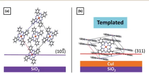
Using this re-determined structure, the peak at 28.1 now corresponds to the (311) plane, which is close to one of the herringbone stacked molecular planes (Fig.4 (a)). As reection geometry (as utilised here) is most sensitive to out-of-plane reections (i.e.the diffraction vector/d* is always normal to the
Fig. 2 (a) AFM height image, (b) 3D render of the same image (c) an XRD pattern of a 15 nm thick CuI/SiO2film (inset shows a view orthogonal to
the (111) plane). The lower panel shows the (d) AFM height image and (e) XRD pattern for a 45 nm thick CuI/SiO2film.
Fig. 3 (a) Series of AFM height images of FePc/CuI bilayers with increasing FePc thickness and (b) the XRD pattern of the 50 nm thickness FePc/CuI/SiO2film.
Open Access Article. Published on 13 June 2014. Downloaded on 11/03/2015 13:47:45.
This article is licensed under a
[image:4.595.47.286.476.689.2]surface), this suggests that the (311) plane is close to parallel to the substrate and therefore the CuI (111) surface.
This implies a molecular orientation in some stacks which isat-lying with respect to the underlying SiO2and CuI (111) layer, with the FePcpsystem projecting out of the CuI (111) plane. Increasing the substrate temperature increases the size of the CuI grains of which thelm was composed, and due to the uniform out-of-plane orientation across thelm this produces larger CuI (111) faces. These faces act as a structural template for the impinging FePc molecules, both controlling the relative orientation of the molecules and increasing the size of the grains by controlling nucleation. Using our re-determined crystal structure the change in orientation can be elucidated as the transition from all molecules edge-on ((101) oriented) to inclusion of face-on ((311) oriented) stacks with respect to the substrate plane (Fig. 5). In both cases (with and without CuI) the single diffraction peaks used to ascertain this could be indexed using the same single crystal structure. This leads us to the conclusion that although the orientation of the molecules with respect to the substrate was altered the crystal structure was dened by the same unit cell.
If the crystal structure of the FePc was unchanged and the (311) plane was completely parallel to the surface an inherent inclination of the molecular plane with respect to the surface would be present at the interface. This is due to the facts that the (311) plane is not perfectly parallel to the molecular plane and the FePc molecule is slightly distorted in the single crystal. However, the diffractometer and experimental geometry used here will detect diffraction from planes close to as well as at surface normal. In this case a situation where the (311) plane was projected out of the surface plane at a slight angle (away from surface normal) and a situation where the molecule is lyingat on top of the CuI/SiO2layer would produce very similar diffraction features. However when volumes of reciprocal space close to the (311) reection were explored, no additional Bragg reections were detected.
One of the molecular stacks present in the single crystal structure adopts an orthogonal orientation with respect to its four neighbouring stacks (see ESI†). This interaction is char-acterized by one of the phenyl rings protruding into the‘bay’ area between the phenyl rings of an adjacent molecule. If one of the molecular stacks was oriented to produceat-lying molec-ular orientation and the herringbone packing arrangement was conserved the molecules in the other stack would stand almost upright with respect to the surface. In this situation the overall out-of-plane orientation of the FePclm is modied but not all of the molecules adopt theat-lying orientation with respect to the surface. In this case a larger (edge-to-edge rather than face-to-face) out-of-surface-plane intermolecular spacing may be expected. Another possibility is that the crystal structure was altered by the CuI layer and the‘standing’molecular stacks are no longer present in the thinlm. Although suggestions of this kind have been made in previous papers concerning structural templating of Pcs,25no experimental proof has been published. In either case the overall out-of-plane orientation of thelm was still completely altered by the insertion of the CuI layer as shown by our XRD patterns.
Experimental
Copper iodide (Sigma Aldrich, UK) was used as received and evaporated from a home built evaporator at 340C at a rate of 0.5A s˚ 1as measured by a calibrated quartz crystal microbal-ance. FePc (Sigma Aldrich, UK) was triply puried by thermal gradient sublimation16 and the resulting crystals were used for growth from a homebuilt evaporator at 375C at a rate of 0.2˚A s1.
Alllms were grown in a custom built ultra-high vacuum (UHV) chamber with a base pressure of 3109mbar in which organic and inorganic materials were sublimed onto ambient and elevated temperature substrates. The substrate tempera-ture was measured using a K-type thermocouple mounted close to the sample and calibrated using an optical pyrometer. Substrates were 1010 mm pieces of thermally oxidised silicon (100) single crystal (IDB technologies, UK) cleaned in acetone, Decon-90®–de-ionised water mix and isopropanol. These were dried in a stream of dry nitrogen and UV–ozone cleaned before being loaded into vacuum.
Fig. 4 –Comparison of the previously published FePc single crystal structure and our redetermination, upper panels show a view down the‘b’axis and parameters are tabulated underneath.
Fig. 5 –Relative molecular orientation of FePc on (a) bare SiO2and (b)
a CuI templating layer. The same unit cell is shown in both cases and planes responsible for the peaks observed in XRD indicated with col-oured lines and labelled.
Paper Journal of Materials Chemistry C
Open Access Article. Published on 13 June 2014. Downloaded on 11/03/2015 13:47:45.
This article is licensed under a
Creative Commons Attribution 3.0 Unported Licence.
[image:5.595.50.286.47.219.2] [image:5.595.45.291.560.681.2]For single crystal X-ray diffraction (XRD) measurements, crystals were grown using a homebuilt thermal gradient subli-mation apparatus with a base pressure of 2 107 mbar. A suitable crystal was selected and mounted on a Mitigen loop with silicon oil on an Oxford Diffraction Xcalibur Gemini diffractometer, equipped with a Ruby CCD area detector, and was held at 293 K during data collection. Using Olex2,17 the
structure was solved with the ShelXS18 structure solution
program using direct methods and rened with the ShelXL18
renement package using least squares minimisation. Thin lm XRD patterns were obtained using a Panalytical X'Pert Pro MRD diffractometer with monochromatic Cu Ka1radiation.
Atomic force microscopy (AFM) images were recorded using an Asylum research MFP-3D in AC mode (tapping mode) using Olympus AC240-TS silicon tips.
Conclusions
We have prepared and characterised CuI thinlm templates and demonstrated morphological control using elevated substrate temperatures during growth. Thelms were highly crystalline with the (111) faces of individual grains parallel to the plane of the SiO2surface, and this structure was unchanged with growth temperature. Although polycrystallinelms were produced the large grain sizes of the crystallites allows their use as model (111) aligned crystalline substrates. These thinlms have been employed to control the molecular orientation and grain size of an evaporated FePc layer concomitantly. Nucle-ation and growth of thin FePclms was strongly affected by the morphology and structure of the underlying CuI layer with single CuI (111) faces seemingly promoting FePc (311) domain growth. Finally, redetermination of the crystal structure of FePc from single crystal XRD measurements has allowed accurate assignment of the structural changes observed in these bilayers. This methodology shows promise for preferentially aligning phthalocyanine molecules for use in organic electronics devices and producing model systems to study the interactions at organic/inorganic interfaces.
Acknowledgements
LAR and TSJ acknowledge support from the Engineering and Physical Sciences Research Council, UK (Grant no. EP/H021388/1). DSK thanks the Science City Research Alliance and the HEFCE strategic development fund fornancial support. The Panalytical® MRD diffractometer used in this research was obtained through the Science City Advanced Materials Project: Creating and Char-acterizing Next Generation Advanced Materials, with support from Advantage West Midlands (AWM) and part funded by the Euro-pean Regional Development Fund (ERDF).
References
1 S. Heutz, R. Cloots and T. S. Jones,Appl. Phys. Lett., 2000,77, 3938.
2 S. M. Bayliss, S. Heutz, G. Rumbles and T. S. Jones, Phys. Chem. Chem. Phys., 1999,1, 3673–3676.
3 W. Wu, L. A. Rochford, S. Felton, Z. Wu, J. L. Yang, S. Heutz, G. Aeppli, T. S. Jones, N. M. Harrison and A. J. Fisher,J. Appl. Phys., 2013,113, 013914.
4 P. Sullivan, T. S. Jones, A. J. Ferguson and S. Heutz,Appl. Phys. Lett., 2007,91, 233114.
5 L. Wang, G. Liu, H. Wang, D. Song, B. Yu and D. Yan,Appl. Phys. Lett., 2007,91, 063511.
6 S. Heutz, C. Mitra, W. Wu, A. J. Fisher, A. Kerridge, M. Stoneham, A. H. Harker, J. Gardener, H.-H. Tseng, T. S. Jones, C. Renner and G. Aeppli,Adv. Mater., 2007,19, 3618–3622.
7 C. H. Cheng, J. Wang, G. T. Du, S. H. Shi, Z. J. Du, Z. Q. Fan, J. M. Bian and M. S. Wang,Appl. Phys. Lett., 2010,97, 083305. 8 T.-M. Kim, H. J. Kim, H.-S. Shim, M.-S. Choi, J. W. Kim and
J.-J. Kim,J. Mater. Chem. A, 2014,2, 8730–8735.
9 B. P. Rand, D. Cheyns, K. Vasseur, N. C. Giebink, S. Mothy, Y. Yi, V. Coropceanu, D. Beljonne, J. Cornil, J.-L. Br´edas and J. Genoe,Adv. Funct. Mater., 2012,22, 2987–2995. 10 I. Hancox, P. Sullivan, K. V. Chauhan, N. Beaumont,
L. a. Rochford, R. A. Hatton and T. S. Jones,Org. Electron., 2010,11, 2019–2025.
11 A. Hoshino, Y. Takenaka and H. Miyaji, Acta Crystallogr., Sect. B: Struct. Sci., 2003,59, 393–403.
12 C. J. Brown,J. Chem. Soc. A, 1968, 2488.
13 R. W. I. de Boer, M. E. Gershenson, A. F. Morpurgo and V. Podzorov,Phys. Status Solidi A, 2004,201, 1302–1331. 14 K. Xiao, Y. Liu, G. Yu and D. Zhu,Appl. Phys. A: Mater. Sci.
Process., 2003,77, 367–370.
15 F. Pan, H. Tian, X. Qian, L. Huang, Y. Geng and D. Yan,Org. Electron., 2011,12, 1358–1363.
16 A. R. McGhie, A. F. Garito and A. J. Heeger,J. Cryst. Growth, 1974,22, 295–297.
17 O. V. Dolomanov, L. J. Bourhis, R. J. Gildea, J. A. K. Howard and H. Puschmann,J. Appl. Crystallogr., 2009,42, 339–341. 18 G. M. Sheldrick,Acta Crystallogr., Sect. A: Found. Crystallogr.,
2008,64, 112–122.
19 H.-S. Shim, H. J. Kim, J. W. Kim, S.-Y. Kim, W.-I. Jeong, T.-M. Kim and J.-J. Kim,J. Mater. Chem., 2012,22, 9077. 20 S. R. Forrest,Chem. Rev., 1997,97, 1793–1896.
21 D. E. Hooks, T. Fritz and M. D. Ward,Adv. Mater., 2001,13, 227–241.
22 J. E. S. Kim, E. Lim, K. Lee, D. Cha and B. Friedman,Appl. Surf. Sci., 2003,205, 274–279.
23 C. Miller, A. Sharoni, G. Liu, C. Colesniuc, B. Fruhberger and I. Schuller,Phys. Rev. B: Condens. Matter Mater. Phys., 2005,
72, 104113.
24 J. Kirner, W. Dow and W. Scheidt, Inorg. Chem., 1976,15, 1685–1690.
25 S. W. Cho, A. DeMasi, A. R. H. Preston, K. E. Smith, L. F. J. Piper, K. V. Chauhan and T. S. Jones, Appl. Phys. Lett., 2012,100, 263302.
Open Access Article. Published on 13 June 2014. Downloaded on 11/03/2015 13:47:45.
This article is licensed under a