1
On-chip light detection using monolithically integrated quantum dot
micropillars
M. M. Karow,
1,a)P. Munnelly,
1T. Heindel,
1,b)M. Kamp,
2S. Höfling,
2,3C. Schneider,
2and S. Reitzenstein
11Institut für Festkörperphysik, Technische Universität Berlin, 10623 Berlin, Germany
2Department of Technische Physik, Universität Würzburg, 97074 Würzburg, Germany
3School of Physics and Astronomy, University of St Andrews, St Andrews KY16 9SS, United Kingdom
We demonstrate the on-chip detection of light using photosensitive detectors based on quantum dot (QD) micropillar
cavities. These microscale detectors are applied exemplarily to probe the emission of a monolithically integrated,
electrically pumped whispering gallery mode microlaser. Light is detected via the photocurrent induced in the
electrically contacted micropillar detectors under reverse-bias. In order to demonstrate the high potential and
applicability of the microdetector presented, we determine the threshold current of an integrated microlaser to be
(54 ± 4) μA, in very good agreement with the value of (53 ± 4) μA inferred from optical data. Within this work we
realize the monolithic integration of a laser and a detector in a single device operating in the regime of cavity-quantum
electrodynamics. Our results thus advance the research on microscale sensor technology towards the few-photon
quantum limit and pave the way for on-chip opto-electronic feedback experiments.
_____________________________
a) Present address: Ferdinand-Braun-Institut, Leibniz-Institut für Höchstfrequenztechnik, Gustav-Kirchhoff-Str. 4, 12489
Berlin, Germany, [email protected]
2
they can act as compact, low-power building blocks in optical communication and information technologies [5-7]. Within these
fields, semiconductor quantum dots (QDs) and QD-microcavity systems show great promise for advancing integrated photonics
not only in terms of light sources, but also with regard to detection. In fact, single-photon detection, crucial to quantum
information processing, has been achieved using QDs in transistor- [8], resonant-tunneling diode- [9], and single-QD-based
devices [10]. Integrating the QDs within a resonator further improves the light detection efficiency as well as the wavelength
selectivity [11] and advances the research in the single-emitter regime of cavity-quantum electrodynamics (cQED) [12].
Regarding the generation of light, micropillar cavities with embedded QDs are particularly viable as integrated, electrically
operated light sources as they exhibit high Q-factors and low mode volumes. As such, they provide cQED-enhanced
light-matter interaction [13-15], which allows for the realization of low-threshold high-β lasers for both vertically-propagating modes
[16] and laterally-propagating whispering gallery modes (WGMs) [17, 18]. Further, due to their laterally directed emission,
WGM microlasers are of special interest in the context of coherent light sources for on-chip quantum optical studies [19] and
the generation of non-classical light [20], as well as for driving optical circuits due to their compatibility with planar photonic
networks [21-23]. Moreover, integrating such lasers with microscale detectors opens up interesting perspectives, such as
wavelength-selective microscale sensing applications and opto-electronic feedback experiments. The latter can lead to chaotic
optical and electrical output behavior enabling, e.g., compact and ultrafast random number generators [24, 25]. In this view,
the integration of laterally coupled laser-detector pairs is highly desirable as it allows for the realization of such opto-electronic
feedback ensembles on a single chip.
In this letter, we report on the integration of a microscale photodetector into a cQED system. The QD-based on-chip
microdetector is applied to characterize the emission from a monolithically integrated WGM microlaser via electrical readout
of the photocurrent. In this configuration, we go a significant step beyond the conventional approach in which individual
micropillars have been used as photosensitive devices under axial light incoupling [12]. In order to demonstrate the potential
of our approach, we use a differential lock-in technique to probe the input-output curve of the integrated microlaser and to
determine its threshold current.
A schematic of the integrated microlaser-photodetector pair is shown in Fig. 1(a). The sample is based on a planar
microcavity structure grown by molecular beam epitaxy on an n-doped (100)-oriented GaAs substrate. Therein, n- and p-doped
distributed Bragg reflectors with 27 and 23 λ/4 AlAs/GaAs mirror pairs are grown below and above an intrinsic GaAs λ-cavity,
respectively. A single layer of self-organized InGaAs QDs (area density ~ 109 cm-2) treated with partial capping and annealing
3
as on-chip coherent light sources (via lasing WGM emission) were patterned by electron-beam lithography and reactive ion
plasma etching. Surrounding the characterized microlaser is a group of five 1.6 µm-diameter peripheral micropillars, separated
from the WGM microlaser by a distance of 15 µm, which act as monolithically integrated photodetectors (cf. inset, Fig. 1(a)).
A planarization step with the polymer bencocyclobutene was followed by the application of Au pads serving as electrical
contacts, with separate p-contacts for the laser bar and the detector bar [27].
The device was mounted on a chip carrier within a liquid-Helium flow cryostat and cooled to 25 K for electrical and
optical characterization. The former was carried out with a source-measurement unit for direct current (DC) injection/bias
application and an optional lock-in amplifier (LIA) providing a sinusoidal reference voltage output. The equivalent circuit
diagram of the experiment can be seen in Fig. 1(b). The optical characterization was carried out in a micro-electroluminescence
(µEL) setup featuring a 20× microscope objective (numerical aperture 0.42), a triple-grating monochromator with a spectral
resolution of 85 µeV, and a liquid-nitrogen cooled charge-coupled device camera.
To compare and validate the results obtained from our on-chip detector concept, the WGM microlaser’s emission was
first characterized in a conventional µEL setup to optically determine the input-output characteristic and the threshold current
in off-chip configuration. For this purpose, the WGM laser emission scattered at marker structures located in the vicinity of the
microlaser was collected via the microscope objective and spectra were recorded for injection currents up to 312 µA (see Fig.
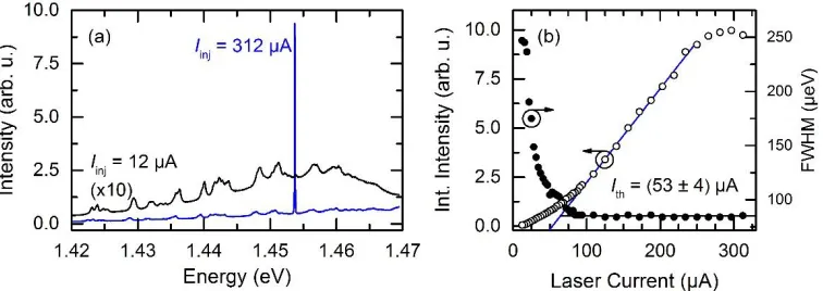
2(a)). The microlaser was found to provide single mode emission at 852.6 nm with a Q-factor of 13,500 at threshold. The lasing
mode was fitted in each case with a Voigt function, taking into account the spectral resolution of the setup, from which the
full-width at half-maximum (FWHM) and integrated intensity were extracted. As seen in Fig. 2(b), at low injection currents, the
WGM mode has a linewidth of 250 µeV. This is followed by a sudden decrease down to the resolution limit of the setup Figure 1: Device layout and electrical circuit used for the measurement of photocurrent from an integrated photodetector. (a) Schematic of the device configuration featuring a whispering gallery mode (WGM) microlaser, which, upon electrical excitation, generates photocarriers in a monolithically integrated peripheral micropillar used as on-chip photodetector. The inset shows a scanning electron micrograph of an exemplary device with the WGM laser and its neighboring photodetectors. (b) This circuit is used to determine the microlaser’s threshold current in a photocurrent extraction experiment in which the biased laser (IWGM) is modulated by a small sinusoidal (AC) signal
[image:3.612.118.499.54.161.2]4
(85 µeV) at elevated currents, indicating the onset of lasing. Likewise, the input-output curve reveals a smooth transition into
linear scaling around threshold. Its value was determined to be Ith = (53 ± 4) µA (at 6.2 V laser bias).
Reverse-biasing the peripheral micropillars allows one to electrically probe the microlaser emission. Once the WGM
microlaser is turned on, the reverse current in the peripheral micropillars increases due to the generation of photocarriers within
the active region. Photocurrent generation was also verified for each microdetector by individual excitation with an external
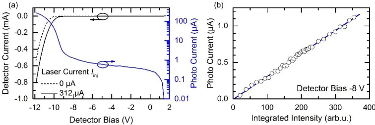
tunable laser (not shown). Fig. 3(a) depicts I-V curves (black) of the peripheral micropillars at no laser current (dashed) and at
312 µA (solid) by a direct measurement of the photocurrent (without LIA). At vanishing laser current, the moderately
reverse-biased detectors show a dark current below 10 nA, while at about -10 V, the junction reaches breakdown. Upon laser emission,
the reverse current increases by the amount of the extracted photocurrent (blue). Its value increases as the detector voltage is
varied from 1.4 (flatband condition) to -9 V, since injected photocarriers are extracted with increasing efficiency from the QD
ensemble due to enhanced tunneling processes [28]. At detector voltages below -9 V, photocarriers are multiplied by impact
ionization, as apparent from the sudden increase in photocurrent. The breakdown voltage of the junction shifts slightly to -9 V,
as a result of the additional impact-ionized photocarriers. This direct operation without the lock-in technique allowed a linear
response to the optical emission (Fig. 2(a)) to be verified, see Fig. 3(b). The responsivity was found to be about 0.05 A/W for
biases up to -8 V. Taking into account the dark current at this working point, this corresponds to a noise-equivalent power
(NEP) of 6.3x10⁻⁹ W/Hz1/2. Further, by considering the effective detector area of the five coupled micropillar detectors, we gain
an upper limit for the specific detectivity of D* = 1x10⁵ cmHz1/2/W. This rather moderate value is explained by the fact, that
our detectors are based on a single low-density layer of InGaAs QDs (areal density ~ 109 cm-2) in the active layer. We expect
that D* can be significantly enhanced by 2-3 orders of magnitude via stacked layers (e.g. 10 layers) of QDs with high areal Figure 2: (a) Two exemplary spectra of the WGM microlaser at an injection current Iinj of 12 and 312 µA
[image:4.612.114.492.55.189.2]5
density (1010-1011) cm-2 in the active region, which would result in a performance comparable to reports on QD [29] and
quantum well [30] -based photodetectors utilizing nanophotonic approaches. Moreover, WGM microlasers with
Limaçon-shaped cross-section, providing in-plane unidirectional emission into two light-cones [21], can strongly enhance the overall
coupling efficiency of the integrated microlaser-microdetector system.
After demonstrating the capability of our highly integrated approach for on-chip photocurrent extraction, we apply this
appealing feature exemplarily to infer the threshold current of the WGM microlaser, being a crucial parameter of coherent light
sources. For this purpose, the circuit shown in Fig. 1(b) is utilized. The LIA allows us to apply a differential acquisition method
which is particularly sensitive to a time-varying lasing mode intensity, as elaborated in the following. It can be inferred from
the right branch of the circuit that the input voltage Vin to the LIA is given by Vin(t)=VD/(1+RD(t)/R), as derived from Kirchhoff’s
law. Here, the detector voltage VD, its resistance RD, and the readout resistance R are introduced. If a small AC modulation with
a frequency ω is added to the constant current IWGM (left branch Fig. 1(b)), RD is reduced according to RD(t)=R0-RPCDC
-RPCAC×sin(ωt), as a result of photo carrier-injection. We introduced the diode’s resistance R0 under no illumination and
appropriate resistance quantities RPCDC and RPCAC accounting for diode resistance-lowering upon injection. The time-varying
input signal Vin(t) is processed by the LIA to the readout voltage VLIA=(1/2√2)×(maxt(Vin)-mint(Vin)). Approximating this
expression in the limit RPCDC/R≪1 and RPCAC/R≪1 yields
𝑉LIA(𝐼WGM) = (𝛼𝑉D/√2) × ∆𝑃opt(𝐼WGM) × (𝛼×𝑃(1+𝑅opt(𝐼WGM)
0/𝑅)3 +
1
(1+𝑅0/𝑅)2) . (1)
[image:5.612.117.495.54.180.2]6
Above threshold (IWGM > Ith), Eq. (1) describes a function linear in IWGM since Popt is a linear function of IWGM and hence
∆Popt(IWGM > Ith) = const. Upon subtraction of this superimposed linear trend in the limit R0/R≫1, one obtains the pseudo-LIA
voltage VLIA†(IWGM)∝VD×(∆Popt(IWGM)-∆Popt(IWGM > Ith)). As the microlaser’s input-output curve Popt(IWGM) can be derived
from
VLIA†(IWGM) by integration,
𝑃LIA = ∫0𝐼WGM𝑉LIA† (𝐼WGM′ )d𝐼WGM′ ∝ 𝑃opt(𝐼WGM) + 𝐶, (2)
[image:6.612.195.431.48.384.2]the value of the laser threshold current is directly accessible.
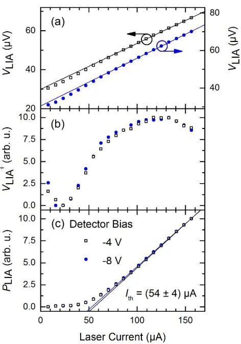
Figure 4: Experimental data for all-electrical threshold-current determination with a phase-sensitive method. Two different configurations with a detector bias of -4 (black squares) and -8 V (blue circles) are used. (a) LIA-output voltage, originating from the time-varying voltage drop across a resistor in series with the photodetector, against the laser current. Linear curves are fitted to the upper branches (laser current greater than 90 µA). (b) Subtracting the linear trend superimposed to VLIA yields this curve, which closely resembles the derivative of
the laser’s input-output curve (normalized). (c) Numerical integration (cf. Eq. (2)) gives the input-output curve
7
In Fig. 4, we display experimental data obtained in two threshold-determination experiments with two exemplary detector
bias voltages VD of -4 and -8 V, respectively (500 Ω readout resistance R) over a range of laser currents between 8 and 160 µA
(3 and 9.5 V laser bias, respectively). The sinusoidal amplitude for the small signal modulation was chosen as 0.1 V at a
frequency of 102 kHz. The LIA readout VLIA which varies with laser current can be inspected in Fig. 4(a). As described
previously (cf. Eq. (1)), VLIA scales linearly with IWGM at high currents. At lower laser currents, the data show a transition into
a linear trend with a clear kink at around 50 µA. This is illustrated by the pseudo-LIA voltage VLIA† shown in Fig. 4(b) for
which this superimposed linear function was subtracted from VLIA. It closely resembles the derivative of the microlaser’s
input-output curve. Numerical integration of VLIA† (cf. Eq. (2)) retrieves the microlaser’s input-output curve as shown in Fig. 4(c).
Linear fits to the high-current branches allow for an extraction of the laser threshold current defined as the abscissa intercept
with the linear functions. In order to verify the result, this experiment was carried out in more than ten different configurations
(R∈[75:10k] Ω and VD∈[-8:0] V) yielding the threshold current (54 ± 4) µA.
In summary, we have demonstrated the realization of on-chip microscale photodetection and its application to characterize
a monolithically-integrated cQED-enhanced device. Using such integrated microdetectors, we all-electrically determined the
threshold current of a WGM microlaser via a lock-in technique. The results presented in this report show promise for the
exploration of self-pulsing and chaos for, e.g., random number generation and chaos-based secure communication, as it is
possible to read out the laser-induced photocurrent and use it to modulate the current flowing through the microlaser in an
on-chip feedback-type experiment. Beyond this, the presented concept of a monolithically integrated microlaser-photodetector
pair might be utilized for on-chip chemical sensing applications. To realize such micro-scale absorption spectroscopy, WGM
lasers emitting in the near-infrared [31] and operating at room temperature [32] can be exploited in future.
ACKNOWLEDGMENTS
This work was supported by the German Research Foundation (DFG) under Grants RE2974/9-1 and SCHN1376/1-1. The
research leading to these results has received funding from the European Research Council under the European Union's Seventh
Framework ERC Grant Agreement No. 615613. The authors gratefully thank M. Lermer, M. Emmerling, and A. Wolf for
expert sample preparation.
REFERENCES
[1] D. Englund, H. Altug, and J. Vučković, Appl. Phys. Lett. 91, 071124 (2007).
8
[3]Kamp, S. Höfling, R. Sanjines, and A. Fiore, Appl. Phys. Lett. 99, 181110 (2011).
[4] G. Reithmaier, S. Lichtmannecker, T. Reichert, P. Hasch, K. Müller, M. Bichler, R. Gross, and J. J. Finley, Sci.
Rep. 3, 1901 (2013).
[5] M. Haurylau, G. Chen, H. Chen, J. Zhang, N. A. Nelson, D. H. Albonesi, E. G. Friedman, and P. M. Fauchet,
IEEE J. Sel. Top. Quantum Electron. 12, 1699–1705 (2006).
[6] A. Shacham, K. Bergman, and L. P. Carloni, IEEE Trans. Comput. 57, 1246 (2008).
[7] L. Thylén and L. Wosinski, Photon. Res. 2, 75–81 (2014).
[8] A. J. Shields, M. P. O’Sullivan, I. Farrer, D. A. Ritchie, R. A. Hogg, M. L. Leadbeater, C. E. Norman, and M.
Pepper, Appl. Phys. Lett. 76, 3673 (2000).
[9] J. C. Blakesley, P. See, A. J. Shields, B. E. Kardynał, P. Atkinson, I. Farrer, and D. A. Ritchie, Phys. Rev. Lett. 94,
067401 (2005).
[10] S. Komiyama, O. Astafiev, V. Antonov, T. Kutsuwa, and H. Hirai, Nature 403, 405 (2000).
[11] C. Kistner, S. Reitzenstein, C. Schneider, S. Höfling, and A. Forchel, Appl. Phys. Lett. 94, 221103 (2009).
[12] P. Gold, M. Gschrey, C. Schneider, S. Höfling, A. Forchel, M. Kamp, and S. Reitzenstein, Phys. Rev. B 86,
161301(R) (2012).
[13] J. M. Gérard, B. Sermage, B. Gayral, B. Legrand, E. Costard, and V. Thierry-Mieg, Phys. Rev. Lett. 81, 1110
(1998).
[14] K. J. Vahala, Nature 424, 839 (2003).
[15] J. P. Reithmaier, G. Sęk, A. Löffler, C. Hofmann, S. Kuhn, S. Reitzenstein, L. V. Keldysh, V. D. Kulakovskii, T.
L. Reinecke, and A. Forchel, Nature 432, 197 (2004).
[16] S. Reitzenstein, A. Bazhenov, A. Gorbunov, C. Hofmann, S. Münch, A. Löffler, M. Kamp, J. P. Reithmaier, V. D.
Kulakovskii, and A. Forchel, Appl. Phys. Lett. 89, 051107 (2006).
[17] V. N. Astratov, S. Yang, S. Lam, B. D. Jones, D. Sanvitto, D. M. Whittaker, A. M. Fox, M. S. Skolnick, A.
Tahraoui, P. W. Fry, and M. Hopkinson, Appl. Phys. Lett. 91, 071115 (2007).
[18] Y.-R. Nowicki-Bringuier, J. Claudon, C. Böckler, S. Reitzenstein, M. Kamp, A. Morand, A. Forchel, and J. M.
Gérard, Opt. Express 15, 17291 (2007).
[19] E. Stock, F. Albert, C. Hopfmann, M. Lermer, C. Schneider, S. Höfling, A. Forchel, M. Kamp, and S.
9
[20] P. Munnelly, T. Heindel, M. M. Karow, S. Höfling, M. Kamp, C. Schneider, and S. Reitzenstein, IEEE J. Sel. Top.
Quantum Electron. 21, 1900609 (2015).
[21] F. Albert, C. Hopfmann, A. Eberspächer, F. Arnold, M. Emmerling, C. Schneider, S. Höfling, A. Forchel, M.
Kamp, J. Wiersig, and S. Reitzenstein, Appl. Phys. Lett. 101, 021116 (2012).
[22] A. W. Schell, J. Kaschke, J. Fischer, R. Henze, J. Wolters, M. Wegener, and O. Benson, Sci. Rep. 3, 1577 (2013).
[23] P. S. Kuo, J. Bravo-Abad, and G. S. Solomon, Nat. Commun. 5, 3109 (2014).
[24] I. Kanter, Y. Aviad, I. Reidler, E. Cohen, and M. Rosenbluh, Nat. Photonics 4, 58 (2010).
[25] M. Sciamanna and K. A. Shore, Nat. Photonics 9, 151 (2015).
[26] J. M. Garcı́a, T. Mankad, P. O. Holtz, P. J. Wellman, and P. M. Petroff, Appl. Phys. Lett. 72, 3172 (1998).
[27] C. Böckler, S. Reitzenstein, C. Kistner, R. Debusmann, A. Löffler, T. Kida, S. Höfling, A. Forchel, L. Grenouillet,
J. Claudon, and J. M. Gérard, Appl. Phys. Lett. 92, 091107 (2008).
[28] F. Hofbauer, S. Grimminger, J. Angele, G. Böhm, R. Meyer, M. C. Amann, and J. J. Finley, Appl. Phys. Lett. 91,
201111 (2007).
[29] S. C. Lee, S. Krishna, and S. R. J. Breuck, Opt. Express 17, 23160 (2009).
[30] S. Kalchmair, R. Gansch, S. I. Ahn, A. M. Andrews, H. Detz, T. Zederbauer, E. Mujagić, P. Reininger, G. Lasser,
W. Schrenk, and G. Strasser, Opt. Express 20, 5622 (2012).
[31] A. Schlehahn, F. Albert, C. Schneider, S. Höfling, S. Reitzenstein, J. Wiersig, and M. Kamp, Opt. Express 21,
15951 (2013).
[32] M. Munsch, J. Claudon, N. S. Malik, K. Gilbert, P. Grosse, J. M. Gérard, F. Albert, F. Langer, T. Schlereth, M. M.