Development of CdSe thin films for application in
electronic devices
OLUSOLA, O. I., ECHENDU, O. K. and DHARMADASA, I
<http://orcid.org/0000-0001-7988-669X>
Available from Sheffield Hallam University Research Archive (SHURA) at:
http://shura.shu.ac.uk/8945/
This document is the author deposited version. You are advised to consult the
publisher's version if you wish to cite from it.
Published version
OLUSOLA, O. I., ECHENDU, O. K. and DHARMADASA, I (2015). Development of
CdSe thin films for application in electronic devices. Journal of Materials Science:
Materials in Electronics, 26 (2), 1066-1076.
Copyright and re-use policy
See http://shura.shu.ac.uk/information.html
Sheffield Hallam University Research Archive
1
DEVELOPMENT OF CdSe THIN FILMS FOR APPLICATION IN ELECTRONIC DEVICES.
O.I. Olusola1*, O.K. Echendu1 and I.M. Dharmadasa1
1Electronic Materials and Sensors Group, Materials and Engineering Research Institute, Sheffield Hallam
University, Sheffield S1 1WB, United Kingdom.
*E-mail: [email protected]; Tel.: +44 114 225 6910; Fax: +44 114 225 6930.
ABSTRACT
Thin films of cadmium selenide (CdSe) have been deposited on fluorine-doped tin oxide (FTO)-coated glass
using potentiostatic electrodeposition method. The suitable range of deposition potentials for the formation of
stoichiometric layer of CdSe was established using cyclic voltammograms. The films have been characterised
using X-ray diffraction (XRD), Raman spectroscopy, optical absorption, scanning electron microscopy (SEM),
atomic force microscopy (AFM) and photo-electrochemical (PEC) cell techniques. XRD results show that the
deposited films are polycrystalline in nature having hexagonal structure with preferred orientation along (002)
plane. PEC study reveals that the films have n-type electrical conductivity. The optical bandgap of the film have
been estimated to be 2.00 and 1.80 eV for as-deposited and heat-treated layers respectively when grown at a
cathodic potential of 1972 mV. The electronic quality of the electrodeposited CdSe layers was also tested using
the device structure glass/FTO/n-CdSe/Au which produced Schottky diodes with rectification factor of 102.9,
reverse saturation current of ~372 nA and threshold voltage of ~0.15 V. The potential barrier observed for
Au/n-CdSe interface is greater than 1.10 eV.
Keywords: Electrodeposition, n-CdSe, Thin Films, Cathodic Potential.
1. INTRODUCTION
CdSe is a well-known II-VI semiconductor that can crystallize in either wurtzite (hexagonal) or the zinc blende
(cubic) structure. It is a direct bandgap semiconductor material which is used in opto-electronic devices,
light-emitting diodes (LEDs), field-effect transistors (FETs), biosensors, biomedical imaging and solar cells
fabrication [1]. CdSe can be used as an n-type buffer, window or absorber layer in thin film solar cells by
selecting its thickness appropriately. It is suitable as a buffer layer because of its unique wetting properties on
glass/fluorine-doped tin oxide (FTO) surfaces. CdSe has a bandgap of ~1.80 eV in the wurtzite crystal phase and
2
wide range of the visible spectrum. The deposition of CdSe thin film has been achieved using different growth
methods such as pulsed laser deposition [2], thermal evaporation [3], chemical bath deposition (CBD) [2, 4-5],
spray pyrolysis [6-7] and electrodeposition [8-12]. Among the above mentioned deposition techniques, the
electrodeposition method is suitable because of its low temperature growth, its low capital cost and the ability to
control the film thickness by varying the deposition time and potential.
Electrodeposition method also provides the platform for controlling the material properties (optical, structural,
morphological and electrical) by adjusting the preparative parameters such as growth temperature of the
electrolyte, pH, concentration of the electrolyte, stirring, deposition time and post-deposition annealing
temperature. One key requirement in electrodeposition technique is that the substrate must be conductive. Golan
et al produced epitaxially oriented arrays of CdSe nanocrystals electrodeposited onto gold substrates [9].
Thanikaikarasan et al have prepared CdSe thin films on indium-doped tin oxide (ITO)-coated glass substrates
from an aqueous electrolyte using a 3-electrode electrodeposition method [13]. Pawar et al used 3-electrode
electrodeposition method to electrosynthesize thin films of CdSe on stainless-steel and FTO-coated glass
substrates from aqueous acidic bath using cadmium acetate as a Cd ion source [14]. Athanassopoulou et al
electrodeposited CdSe films on nickel substrates using a thermostat-controlled three-electrode cell [15]. CdSe
thin films were also electrodeposited by Lokhande et al on titanium substrates from aqueous and weakly
alkaline bath using a three-electrode cell [11].
Several works have been carried out to-date on electrodeposition of CdSe thin films using three-electrode cell
from aqueous and non-aqueous solution in either acidic or basic medium. Substrates such as ITO-coated glass,
FTO-coated glass, nickel, stainless steel, titanium and so on have also been used as conductive substrates to
carry out electroplating work. This work focuses on cathodic electrodeposition of CdSe thin films on
FTO-coated glass substrates using two-electrode system and aqueous acidic electrolyte. Electronic qualities of the
electrodeposited CdSe layers were also tested using the device structure glass/FTO/n-CdSe/Au metal contact.
2. EXPERIMENTAL DETAILS
2.1 Electrodeposition of CdSe Layers
The precursors used for the growth of CdSe thin films were 0.3M CdCl2 as Cd2+ source and 0.003M SeO2 as
Se2- source in 400 ml of deionised water. All chemicals used for electrodepositon were analytical reagent grade
of purity 5N (99.999%) from Sigma Aldrich. The growth temperature and pH of the bath used for the
3
was adjusted accordingly by adding ammonia or HCl solution. The glass/FTO used in this work was TEC-15
with a sheet resistance of 13 Ω/□. Since substrate cleaning is a very important step in thin films deposition, the
glass substrates were thoroughly cleaned using soap solution and organic solvents (methanol and acetone).
Samples were also rinsed with de-ionised water in between solvents; finally, the substrates were dried with
nitrogen gas. The electroplating of CdSe was carried out in potentiostatic mode using a 2-electrode system
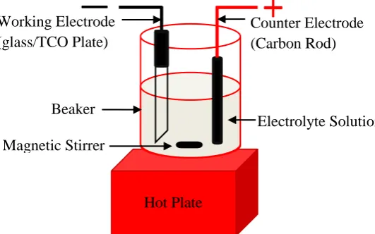
which is known for its low-cost and impurities reduction in the electrolytic bath [16-17]. Fig. 1 shows the
[image:4.595.150.416.234.400.2]typical electrodeposition set-up for the simplified 2-electrode system.
Fig. 1. Electrodeposition set-up used for a simplified 2-electrode system.
2.2 Experimental Techniques
The films were characterised for their structural properties by using Philips PW 3710 X'pert Pro diffractometer
(Philips Analytical, Almelo, The Netherlands) with Cu-Kα monochromator of wavelength, λ= 1.5416 Å in the
range of 2θ = (10 - 70)o. The X-ray generator tension and current were 40 kV and 40 mA respectively. The
surface morphology of the deposited films was studied with scanning electron microscopy (SEM) by using FEI
NOVA 200 NanoSEM equipment. Atomic force microscopy (AFM) was carried out by the collaborator in
Kazakhstan. A Carry 50 scan UV-Visible spectrophotometer (Varian Australia Pty. Ltd.) was used for studying
the optical properties of the deposited films and for bandgap estimation, while thickness measurement on the
deposited layers was carried out using UBM Microfocus optical measuring system (UBM, Messetechnik
GmbH, Ettlingen, Germany).
A computerised GillAC potentiostat was used to carry out the cyclic voltammetry and electrodeposition while
photoelectrochemical (PEC) cell measurements were carried out to determine the electrical conductivity type of
the electrodeposited (ED) CdSe. The PEC cell consists of a graphite electrode which acts as the counter
electrode, the semiconducting electrode (FTO/CdSe) to form the active junction and electrolyte made from
Magnetic Stirrer
Beaker
Working Electrode
(glass/TCO Plate)
Electrolyte Solution
Counter Electrode
(Carbon Rod)
4
aqueous solution of 0.10M Na2S2O3. By immersing the semiconducting electrode inside the electrolyte, a
solid/liquid junction is formed. The difference between the voltages when the semiconductor is illuminated (VL)
and when the semiconductor is in dark condition (VD) represents the PEC signal or open circuit voltage that is
produced by the solid/liquid junction. The light source is a DC 12 V, 5 W tungsten filament bulb. The sign of
the PEC signal determines the electrical conductivity type while the magnitude of the PEC signal indicates the
quality of the depletion layer formed at the interface [17].
3. RESULTS AND DISCUSSION
3.1 Cyclic Voltammetry
Cyclic voltammetry is a very useful tool in electrochemistry to determine the suitable voltage range for growing
thin film materials [18]. In this process, a range of cathodic potentials from 0 mV to 2500 mV was applied
across the electrolyte through the electrodes, using a computerised potentiostat at a sweep rate of 180 mVmin-1.
The current through the electrolyte was monitored as the voltages between electrodes are changed. Cyclic
voltammetry was used to monitor the electrochemical reactions in solutions of 0.3M CdCl2, 0.003M SeO2 and
0.3M CdCl2 + 0.003M SeO2 each in 400 ml of de-ionised water to determine the approximate deposition
voltages for Cd, Se and CdSe respectively.
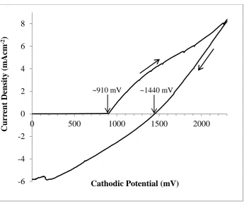
3.1.1 Cyclic voltammogram of 0.3M CdCl2
0.3M CdCl2 was prepared using 400 ml of de-ionised water and the pH of the first solution was measured to be
3.79 ± 0.02 at room temperature; this pH was adjusted to 2.20 ± 0.02 by the addition of HCl solution. The first
voltammogram of the CdCl2 solution as shown in Fig. 2 was taken to help in determining the potential at which
the Cd deposition and dissolution take place. From Fig. 2, the first hump appears at a cathodic potential ~910
mV; this shows that Cd begins to deposit at this potential. In the reverse direction of the curve, the transition
point from the positive current density axis to the negative is ~1440 mV; this voltage is an indication of the
potential at which Cd dissolution begins to dominate. In fact, at ~1440 mV, equal amounts of Cd deposition and
dissolution take place and hence the resultant current becomes zero. The reduction of Cd2+ to Cd on the surface
of FTO electrode takes place according to Eqn. (1), and the current flow is in the forward direction. However,
the dissolution of Cd takes place according to Eqn. (2) and the current produced is in the opposite direction.
5
[image:6.595.76.422.99.391.2]Cd → Cd2+ +2e- (2)
Fig. 2. A typical cyclic voltammogram of electrolyte containing 0.3M of CdCl2 aqueous solution (pH = 2.20 ±
0.02, T = 80oC).
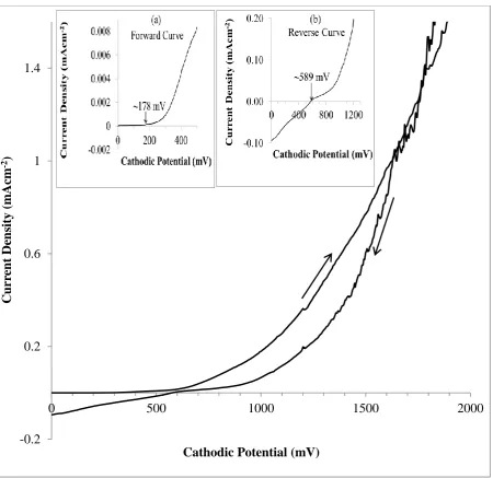
3.1.2 Cyclic voltammogram of 0.003M SeO2
A cyclic voltammogram of 0.003M SeO2 solution is shown in Fig. 3. In the forward curve (Fig. 3a), the first
hump appears at a cathodic potential ~178 mV; this voltage is an indication of the potential at which Se
deposition begins. According to Pawar et al, this reduction peak is due to the irreversible reaction shown in Eqn.
(3b) [14]. Se dissolution begins to dominate at approximately 589 mV as shown in Fig. 3b.
SeO2 + H2O → H2SeO3 (3a)
H2SeO3 + 4H+ + 4e- →Se + 3H2O (3b)
-6
-4
-2
0
2
4
6
8
0
500
1000
1500
2000
Curr
en
t
De
n
sity (
m
Ac
m
-2
)
Cathodic Potential (mV)
6
Fig. 3. A typical cyclic voltammogram of electrolyte containing 0.003M of SeO2 aqueous solution (pH = 2.20 ±
0.02, T = 80oC).
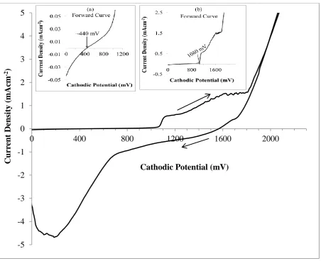
3.1.3 Cyclic voltammogram of 0.3M CdCl2 + 0.003M SeO2
Fig. 4 shows the cyclic voltammogram measured for glass/FTO electrode in an aqueous solution containing a
mixture of 0.3M CdCl2 and 0.003M SeO2. It is also worth noting that the minimum standard reduction potential
for electrolysis of water molecules is about 1230 mV [19]. The discharging of most active H atoms at the
cathode while CdSe is forming is an excellent built-in method to passivate defects in the CdSe layer. However,
if H2 bubbles are formed at the cathode, it could have a detrimental effect of delamination of the semiconducting
layer.
-0.2
0.2
0.6
1
1.4
0
500
1000
1500
2000
Curr
en
t
De
n
sity (
m
Ac
m
-2
)
7
The forward curve illustrated in Fig. 4a shows that Se begins to deposit at ~440 mV while Fig. 4b shows that Cd
begins to deposit at ~1080 mV. The sudden rise in deposition current at 1080 mV to 1800 mV shows the
beginning of reaction between Cd and Se to form CdSe. In this region, the layer formed is a mixture of CdSe
and elemental Se thus giving rise to a Se-rich CdSe layer. Beyond 1800 mV, a sharp rise is noticed in the
deposition current. This leads to a gradual decrease in the amount of elemental Se because more Cd is
incorporated into the CdSe layer. As the growth voltage further increases, the amount of elemental Se in the
CdSe layer gradually reduces thus giving rise to stoichiometric formation of CdSe layer in the voltage range
between 1900 to 2000 mV. Beyond 2000 mV, formation of Cd dendrites was observed. The Cd dendrites
formation shows that at voltages ≥2000 mV, the CdSe layer formed is a Cd-rich material.
The formation of CdSe thin film is according to the following overall reactions:
CdCl2.H2O → Cd2+ + 2Cl- +H2O (4a)
SeO2 + H2O → H2SeO3 (4b)
H2SeO3 + 4H+ + 6e- →Se2- + 3H2O (4c)
Reaction for the formation of CdSe on FTO substrate may be due to Eqn. (5).
Cd2+ + Se2- → CdSe (5)
As seen from Figs. 2 and 3, Cd begins to deposit at around 910 mV while Se begins to deposit at around 178
mV under the experimental conditions used in this work. The shift in the reduction potential of both Cd and Se
from ~910 mV and 178 mV (Figs. 2 and 3) to ~1080 mV and 440 mV (Figs. 4b and 4a) respectively may be due
to the chemical reaction that takes place to form CdSe. Comparing the potential at which both Cd and Se begin
to deposit, it can be seen that Se deposits first before Cd as seen from the cyclic voltammogram. The redox
potential (Eo) of Se and Cd are +0.74 and -0.40 respectively [20]. From the redox potential values, Se shows a
more positive redox potential than Cd and therefore deposits first. The theoretical redox potential value can be
used to determine which of the elements deposit first; however, its shortcoming is that it cannot be used to
determine the approximate potential at which the compound is formed. This is why cyclic voltammetry was
8
Fig. 4. Cyclic voltammogram of electrolyte containing 0.3M of CdCl
2 + 0.003M of SeO2 aqueous solution (pH
= 2.20 ± 0.02, T = 80oC). (Insets show the transition voltages).
3.2 Material Characterisation
The three techniques; XRD, optical absorption and PEC cell measurements were used in the preliminary
characterisation and optimisation of growth voltage of the CdSe layers. To obtain a suitable deposition potential
for the CdSe layer, other preparative parameters such as the growth temperature, pH and growth time (tg) were
kept constant at 80oC, 2.20 ± 0.02 and five minutes respectively.
3.2.1 X-ray diffraction (XRD) studies
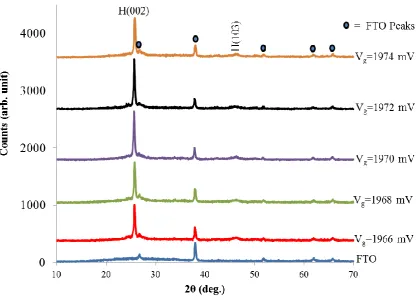
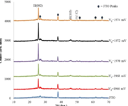
Samples of CdSe layers were grown in the voltage range between 1900 mV and 2000 mV in order to examine
their structural properties and to identify material phases. This allows preliminary optimisation of growth
voltage, Vg to produce near stoichiometric CdSe. Typical XRD patterns for as-deposited (AD) CdSe as a
function of Vg are shown in Fig. 5 while Fig. 6 shows the XRD patterns of heat-treated (HT) CdSe in air at
-5
-4
-3
-2
-1
0
1
2
3
4
5
0
400
800
1200
1600
2000
Curr
en
t
De
n
sity (
m
Ac
m
-2
)
9
350oC for 15 minutes. The XRD results thus show that CdSe layer grows best in the cathodic voltage range
between 1966 and 1974 mV. A continuous increase in peak intensity was observed as the cathodic deposition
voltage increases from 1960 to 1972 mV. A further increase in the voltage led to a decrease in the peak intensity
indicating decrease in crystallinity in this Vg region. The XRD results also show that the highest intensity of the
(002) peak occurs at a cathodic potential of 1972 mV for both AD- and HT-CdSe samples (see Fig. 7).
Therefore, in this work, Vg of 1972 mV was selected as the optimum potential for electrodeposition of CdSe
thin films. The XRD peaks also show that the as-grown and annealed CdSe films are polycrystalline in nature
having hexagonal structure with the preferred orientation along (002) plane. Other peaks that correspond to
[image:10.595.77.496.295.601.2](103) and (112) planes are also observed with lower peak intensities.
10
Fig. 6. XRD patterns for heat-treated CdSe layers at 350oC for 15 minutes in air, as a function of growth
voltage, Vg.
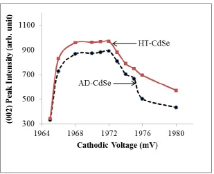
Fig. 7 shows how the intensity of the (002) peak varies with the cathodic potential for both AD- and HT-CdSe.
This result also explains how the crystallinity of the CdSe layers is improved when subjected to heat treatment.
The peak intensities of the HT-CdSe are generally higher than those of the AD-CdSe. This is because increase in
temperature also increases the grain size of the CdSe layers thereby leading to a corresponding improvement in
[image:11.595.79.521.80.445.2]11
Fig. 7. Variation of (002) peak intensity as a function of growth voltage for AD- and HT-CdSe layers.
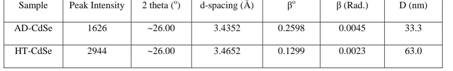
The observed d-spacing values (Table I) from XRD results are compared with the standard values reported in
JCPDS data, reference code '01-077-2307' and both are found to be in good agreement. The crystallite sizes of
the AD- and HT-CdSe grown at 1972 mV for 20 minutes are determined using Scherrer's equation given in Eqn.
(6). This relationship is useful in calculating the crystallite size of a thin film material by using the results
obtained from XRD analysis [13].
cos
9
.
0
D
(6)where D is the crystallite size in nm, λ is the X-ray wavelength (1.5416 Å), θ is the Bragg’s angle in degree and
β is the full width at half maximum (FWHM) of the peak with highest intensity, measured in radian. However,
the Scherrer’s equation has limitation since it cannot be used to estimate crystallite sizes more than (100-200)
nm [21].
The calculated crystallite sizes for AD- and HT-CdSe thin films using (002) peak were ~33 and 63 nm
respectively. Table I shows the comparison between the peak intensity and FWHM of AD- and HT-CdSe layers
obtained from XRD measurements. After annealing, the intensity increases and the FWHM decreases indicating
12
leads to an increase in the crystallite size and hence, a corresponding increase in grain size. Thus, the higher the
[image:13.595.68.533.152.225.2]crystallite sizes of a thin film material, the better its crystallinity.
Table I. Summary of XRD measurement results for AD- and HT-CdSe layers
Sample Peak Intensity 2 theta (o) d-spacing (Å) βo β (Rad.) D (nm)
AD-CdSe 1626 ~26.00 3.4352 0.2598 0.0045 33.3
HT-CdSe 2944 ~26.00 3.4652 0.1299 0.0023 63.0
3.2.2 Raman spectroscopy measurements
Raman spectroscopy is another technique that can be used in determining the crystallinity of semiconductor
material. The Raman spectra were obtained using a Renishaw Raman microscope with 514 nm argon ion laser
source and a charge-coupled device (CCD) detector. An extended spectrum for the as-deposited (AD) and
heat-treated (HT) CdSe layers was collected at room temperature using a 50% laser power (~15 mW) and 100x
objective in the Raman microscope for 10 seconds. Initially, a 100% laser power (~30 mW) was used in the
experiment but after switching to white light, it was observed that a section of the sample exposed to the beam
was already damaged. For this reason, the laser power was reduced to 50%. Thus, the 50% laser power was able
to reduce the heating effect of the laser beam thereby preventing any change on the layer which could lead to
loss or reduction of crystallinity. Curve fitting was also performed on the spectra using a combination of
Lorentzian/Gaussain mathematical function to obtain parameters such as peak position, peak intensity and peak
width also known as full width at half maximum (FWHM).
Fig. 8 shows two visible Raman peaks for AD- and HT- CdSe layers at 200oC for 10 minutes in air. These peaks
are Raman longitudinal optical (LO) vibration mode at wave numbers 206 cm-1 and 414 cm-1 for 1LO and 2LO
peaks respectively. The wave numbers obtained in this experiment is almost similar to that obtained by Brioude
et al after using an excitation wavelength of 514.5 nm from an argon-krypton laser power [22]. Both AD- and
HT- CdSe thin films reveal clear peaks at 1LO and 2LO with no shift in the peak positions. Table II shows the
parameters obtained after performing curve fitting on the spectra. The result shows that HT-CdSe layer
possesses a better crystallinity than the AD- CdSe layer due to reduced FWHM and higher peak intensity as
13
Fig. 8: Raman spectra of as-deposited and heat-treated CdSe thin films at200oC for 10 minutes in air.
Table II: Raman parameters obtained by curve fitting of the CdSe spectra.
As- Deposited Heat-treated
1LO 2LO 1LO 2LO
Raman peak position (cm-1) 206 414 206 414
Peak intensity (arb. unit) 3002 428 3171 450
FWHM (cm-1) 18.66 30.59 17.67 30.53
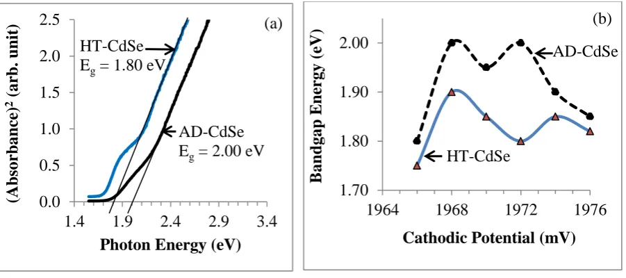
3.2.3 Optical absorption studies
The optical absorption measurements of the ED-CdSe layers were carried out in order to estimate the optical
bandgap energy (Eg). Typical optical absorption graphs for estimation of bandgap energy of both AD- and
HT-CdSe are shown in Fig. 9(a); the graph was obtained by plotting the square of absorbance (A2) as a function of
the photon energy (hѵ). The bandgaps were estimated by extrapolating the straight line portion to the photon
energy axis (at absorbance2 = 0). Fig. 9(b) shows the variation of the bandgap energy with the cathodic potential
for both as-deposited and heat-treated CdSe layers. The results further show that the bandgap energy of the
0
1000
2000
3000
4000
5000
6000
100
200
300
400
500
600
700
800
In
te
n
sity (
ar
b
. u
n
it)
Raman shift (cm
-1)
1LO
[image:14.595.72.494.425.542.2]14
annealed CdSe at a cathodic voltage of 1972 mV tends to be closer to the bandgap of bulk CdSe in the wurtzite
crystal phase. This value has been reported by Zhao et al to be ~1.80 eV [1].
Fig. 9. (a) Typical optical absorption graphs for CdSe layers grown at 1972 mV and (b) Variation of the
bandgap energy as a function of cathodic deposition potential.
3.2.4 Photoelectrochemical (PEC) cell measurements
Fig. 10 illustrates the PEC signal for both AD- and HT-CdSe layers grown at different growth voltages (Vg).
The PEC signal shows that both AD and HT samples of CdSe layers grown in the voltage range of 1966 mV to
1976 mV are n-type in electrical conduction. The result also shows a crossing /overlapping of the PEC signals
for both AD- and HT-CdSe layers at a cathodic potential of 1972 mV. This may be an indication of Vg for
growing stoichiometric CdSe layers.
0.0
0.5
1.0
1.5
2.0
2.5
1.4
1.9
2.4
2.9
3.4
(A
b
sorban
ce
)
2
(ar
b
. u
n
it)
Photon Energy (eV)
HT-CdSe
E
g= 1.80 eV
AD-CdSe
E
g= 2.00 eV
(a)
1.70
1.80
1.90
2.00
1964
1968
1972
1976
B
an
d
gap
E
n
er
gy (e
V)
Cathodic Potential (mV)
AD-CdSe
HT-CdSe
[image:15.595.73.524.127.327.2]15
Fig. 10. Variation of PEC signals for CdSe/electrolytic junctions as a function of growth voltage, indicating
n-type electrical conduction.
3.2.5 Scanning electron microscopy (SEM)
Scanning electron microscopy (SEM) was used to investigate the surface morphology, the range of the grain
sizes and the average thickness of CdSe layer grown on FTO substrates. SEM is a useful tool to study
microstructure of thin films [14]. Fig. 11(a) shows that the surface of AD-CdSe film is uniformly covered by
large numbers of spherical grains without pinholes. The obtained micrographs of AD-CdSe layers reveal
compact films of regular morphology. Fig. 11(b) shows the presence of pinholes on the surface of the HT film;
these pinholes are due to sublimation of excess Se element in the CdSe layer that arises as a result of the high
annealing temperature of 380oC for longer duration of 30 minutes.
-160
-140
-120
-100
-80
1964
1968
1972
1976
P
E
C
S
ign
al
(m
V)
Cathodic Potential (mV)
AD-CdSe
16
Fig. 11. SEM images of CdSe thin films on FTO substrates grown at Vg = 1972 mV and tg = 30 mins. Surface
morphology of (a) AD-CdSe and (b) CdSe heat-treated at 380oC for 30 minutes in air.
Figs. 12(a) and (b) show the SEM images of AD- and HT-CdSe grown at a shorter duration of five minutes. In
Fig. 12(a), the grain size of the AD-CdSe layer ranges from 27 to 320 nm while in Fig. 12(b), the grain size of
HT-CdSe layer ranges from 72 to 360 nm. The minimum and maximum grain sizes of HT-CdSe are greater than
those of the AD-CdSe. This increase in grain size may be attributed to the annealing parameters (temperature
and time) used. Both images show that the whole surface of the substrate is more compact together with absence
of pinholes. The SEM cross-section illustrated in Fig. 13 gives the average film thickness of CdSe layer as 156
nm comparable with the theoretical value of 154 nm which was calculated using Faraday’s laws of electrolysis.
The thickness of SiO2 and FTO from Fig. 13 are 18 nm and 196 nm respectively.
17
Fig. 12. SEM images of CdSe thin film on FTO substrate grown at Vg = 1972 mV for tg = 5 mins. (a) Surface
morphology of AD-CdSe with grain size ranging from 27 to 320 nm and (b) Surface morphology of HT-CdSe at
250oC for 10 minutes in air with grain size ranging from 72 to 360 nm.
Fig. 13. Cross-section of CdSe thin film grown on FTO substrate and heat-treated at 250 oC for 10 minutes in air
(V
g = 1972 mV and tg = 5 mins.) (Courtesy: G.J. Russel microscopy center at University of Durham, UK).
(a)
(b)
CdSe
FTO
[image:18.595.105.481.464.686.2]18
3.2.6 Atomic force microscopy (AFM)Fig. 14 shows AFM pictures of annealed CdSe deposited at 1972 mV on glass/FTO substrates. The AFM
images reveal the presence of large and dense agglomeration of small grains with good cementing effect. The
layers produce pinholes free material suitable for buffer, window and absorber materials in thin film solar cells.
Fig. 14. Typical AFM images of annealed ED-CdSe grown at 1972 mV on glass/FTO substrate (Courtesy:
Institute of Organic Catalysis and Electrochemistry, Almaty, Kazakhstan).
3.2.7 Thickness of ED-CdSe layers
A fore knowledge of thickness of thin film materials is important before device fabrication. This is essential
because thickness affects device performance most especially in thin film solar cells. CdSe can be used as an
n-type buffer, window or absorber layer in thin film solar cells by selecting its thickness appropriately. In this
study, different thicknesses of cadmium selenide were obtained by using deposition times in the range (5 – 30)
minutes at a constant deposition potential of 1972 mV. The thicknesses obtained by using Microfocus Optical
Thickness Profilometer measurement system was compared with the theoretical estimate obtained using
Faraday's laws of electrolysis as illustrated in Fig. 15. Faraday’s law used in the theoretical thickness estimation
is given by Eqn. (7) [23].
nF
JtM
[image:19.595.75.502.184.391.2]19
where T is the thickness of the CdSe film, J is average deposition current density, F is Faraday’s constant, t is
the deposition time, M is the molecular weight of CdSe, n is the number of electrons transferred in the reaction
for the formation of 1 mole of CdSe (n = 6 as given by Eqns. 4(a), 4(b), 4(c) and (5)) and ρ is the density of
CdSe.
Fig. 15 shows that the thickness of AD-CdSe increases as the deposition time increases. The result shows an
approximate linear variation of thickness with deposition time for the experimental curve while in the theoretical
curve, a non-linear response is observed. This non-linear behaviour may be due to variation of current density
with deposition time during growth period. As shown in Fig. 15, the thickness of ED-CdSe layer grown for 15
minutes shows a value of approximately 0.80 μm (800 nm) when measured using the thickness profilometer
while the theoretical estimate using Faraday's equation gave an approximate value of 0.95 μm (950 nm). The
discrepancy between the theoretical estimate and measured value may be due to the fact that not all the
electronic charges used in the theoretical estimate are actually involved in the deposition of CdSe. Part of these
electronic charges flow through the electrolyte to take part in the electrolysis of water; hence, the observed
thicknesses from experimental results are lower than the theoretical values [23]. One of the main advantages of
CdSe is the growth of 2.0 µm layer in a short period of ~30 minutes. This is a very important factor for lowering
the manufacturing cost of solar cells.
Fig. 15. Estimated experimental and theoretical values of thickness for CdSe layers as a function of growth
period.
0.0
0.5
1.0
1.5
2.0
2.5
0
10
20
30
T
h
ickn
ess
(µm
)
Time (minutes)
Theoretical
[image:20.595.76.459.457.685.2]20
3.3 Testing of Electronic Quality of ED-CdSe LayersIn order to test the electronic quality of ED-CdSe layers, Schottky barrier diodes of the structure
glass/FTO/n-CdSe/Au (Fig. 16(a)) were fabricated and tested using current-voltage (I-V) technique. Fig. 16(b) shows the
energy band diagram for the metal semiconductor (MS) structure formed at n-CdSe/Au interface. The potential
barrier height formed at the junction between the CdSe semiconductor and Au metal contact is also illustrated.
CdSe layers grown for durations less than or equal to 5 minutes were very transparent thus allowing them to be
used as buffer and window layers. However, no diode behaviour was observed when the CdSe layers were
grown for this short duration. For this reason, the growth duration was further optimised to find a suitable time
to grow CdSe layers that produce diodes with good rectification property. A good Schottky diode behaviour
with high rectification factor was observed at 20 minutes growth time. For this growth time, film thickness is
~1.6 µm. The log-linear and the linear-linear I-V graphs under dark condition for the Schottky diodes are
illustrated in Figs. 17(a) and (b) respectively.
The rectifying properties were produced by n-CdSe layers grown for 20 minutes, and heat treated at 200oC for
10 minutes in air. Under these growth conditions, the Schottky barriers produced showed rectification factor
(R.F.) ~102.9, ideality factor (n) in the range 1.44 - 2.57, potential barrier height (Φb) greater than 1.10 eV, series
resistance (Rs) ~625 Ω, shunt resistance, (Rsh) →∞, reverse saturation current (Io) ~372 nA and threshold
voltage ~0.15 V. The I-V results observed under AM1.5 (Air-Mass 1.5) illumination for glass/FTO/n-CdSe/Au
structure reveal the photovoltaic activity of the Schottky barrier interface. The initial solar cell parameters
observed are: Voc = 0.28 V, Jsc = 1.68 mA/cm2 and FF = 0.40. These properties indicate that electroplated CdSe
layers possess electronic device qualities and our future research is directed towards development of thin film
21
Fig. 16. (a) Schematic diagram of the n-CdSe/Au Schottky diodes and (b) Energy band diagram of n-CdSe/Au
[image:22.595.83.523.78.244.2]Schottky diodes.
Fig. 17. I-V Characteristics of n-CdSe/Au Schottky diodes under dark conditions (a) The log-linear I-V and (b)
the linear-linear I-V.
4. CONCLUSION
The experimental results presented in this paper show that CdSe can be successfully grown using a 2-electrode
system. XRD results have shown that the layers are hexagonal and polycrystalline with preferential orientation
along the (002) plane. Depending on the thickness of the layer, CdSe can be useful in thin film PV development
for use as a window, buffer or absorber material. PEC study reveals that the films have n-type electrical
conductivity. The results obtained from the optical absorption measurement show that ED-CdSe layers have
(a)
(b)
[image:22.595.87.492.309.559.2]
22
direct band gaps in the range (1.80 - 2.00) eV for as-deposited and (1.75 - 1.90) eV for heat-treated thin films.
n-CdSe/Au Schottky barriers show the electronic device quality of ED-CdSe layers. The wetting property of
compounds containing Se and the ability of the CdSe layer to grow within a very short period of time with good
electronic quality thus make it very attractive in thin film solar cell development. Work is continuing to develop
multi-layer graded bandgap solar cells incorporating electroplated CdSe layers.
ACKNOWLEDGEMENT
The authors would like to acknowledge Stuart Creasey of MERI, Sheffield Hallam University, UK and Leon
Bowen of Physics Department, Durham University, UK for carrying out SEM measurements. Margarita
Dergecheva of Inst. of Organic Catalysis and Electrochemistry, Almaty, Kazakhstan is also thanked for carrying
out AFM measurements. The contributions made by Paul Bingham, Fijay Fauzi, Hussein I. Salim, Azlian
AbdulManaf and Mohammad Madugu are greatly appreciated. The principal author wishes to thank the
Commonwealth Scholarship Commission and Sheffield Hallam University for financial support to undertake
this research. The Federal University of Technology, Akure, Nigeria is also acknowledged for their support.
REFERENCES
1. L.J. Zhao, L.F. Hu, X.S. Fang, J. Adv. Funct. Mater. 22, 1551-1566 (2012).
2. M.A. Hernandez-Perez, J. Aguilar-Hernandez, G. Contreras-Puente, J.R. Vargas-Garcı´a, E.
Rangel-Salinas, Physica E 40, 2535–2539 (2008).
3. Kriti Sharma, Alaa S. Al-Kabbi, G.S.S. Saini, S.K. Tripathi, Materials Research Bulletin 47, 1400–
1406 (2012).
4. S.S. Kale, C.D. Lokhande, Mater. Chem. Phys. 62, 103 (2000).
5. P.P. Hankare, V.M. Bhuse, K.M. Garadkar, S.D. Delekar, I.S. Mulla, Semicond. Sci. Technol. 19, 70
(2004).
6. T. Elango, V. Subramanian, K.R. Murali, Surf. Coat. Technol. 123, 8-11 (2000).
7. A.A. Yadav, M.A. Barote, E.U. Masumdar, Mater. Chem. Phys. 121, 53-57 (2010).
8. S.J. Lade, M.D. Uplane, C.D. Lokhande, Mater. Chem. Phys. 68, 36 (2001).
9. Y. Golan, L. Margulis, I. Rubinstein, G. Hodes, Langmuir 8(3), 749-752 (1992).
10. E. Benamar, M. Rami, M. Fahoume, F. Chiraibi, A. Ennaoui, Ann. Chim. Sci. Mater. 23, 369 (1998).
23
12. S. Thanikaikarasan, T. Mahalingam, M. Raja, Taekyu Kim, Yong Deak Kim, J. Mater. Sci. Mater.
Electron 20, 727-734 (2009).
13. S. Thanikaikarasan, K. Sundaram, T. Mahalingam, S. Velumani, Jin-koo Rhee, J. Mater. Sci. Eng. B
174, 242-248 (2010).
14. S.M. Pawar, A.V. Moholkar, K.Y. Rajpure, C.H. Bhosale, J. Phys. & Chem. of Solids 67,
2386-2391 (2006).
15 M.D. Athanassopoulou, J.A. Mergos, M.D., Palaiologopoulou, Th.G. Argyropoulos, C.T. Dervos, Thin
Solid Films 520, 6515-6520 (2012).
16. I.M. Dharmadasa, J. Haigh, J. Electrochem. Soc. 153(1), G47-G52 (2006).
17. I.M. Dharmadasa, R.P. Burton, M. Simmonds, Sol. Energy Mater. Sol. Cells 90, 2191-2200 (2006).
18. Y.G. Gudage, N.G. Deshpande, R. Sharma, J. Phys. & Chem. of Solids 70, 907-915 (2009).
19. J. Sun, D.K. Zhong, D.R. Gamelin, Energy Environ. Sci. 3, 1252-1261 (2010).
20. S.G. Bratsch, J. Phys. Chem. Ref. Data 18(1), 1-21 (1989).
21. H. Uwe, G. Neil, Nature Nanotechnology 6, 534 (2011).
22. A. Brioude, J. Bellessa, S. Rabaste, B. Champagnon, L. Sphanel, J. Mugnier, J.C. Plenet, J. Appl. Phys.
95(5), 2744-2748 (2004).
23. F. Fauzi, D.G. Diso, O.K. Echendu, V. Patel, Y. Purandare, R. Burton, I.M. Dharmadasa, Semicond.