warwick.ac.uk/lib-publications
Original citation:
Chan, Chun Wa, Li, Fan, Sanchez, Ana M., Mawby, P. A. (Philip A.) and Gammon, P. M..
(2017) Comparative study of RESURF Si/SiC LDMOSFETs for high-temperature applications
using TCAD modeling. IEEE Transactions on Electron Devices, 64 (9). pp. 3713-3718.
Permanent WRAP URL:
http://wrap.warwick.ac.uk/91921
Copyright and reuse:
The Warwick Research Archive Portal (WRAP) makes this work of researchers of the
University of Warwick available open access under the following conditions.
This article is made available under the Creative Commons Attribution 3.0 (CC BY 3.0) license
and may be reused according to the conditions of the license. For more details see:
http://creativecommons.org/licenses/by/3.0/
A note on versions:
The version presented in WRAP is the published version, or, version of record, and may be
cited as it appears here.
Comparative Study of RESURF Si/SiC
LDMOSFETs for High-Temperature
Applications Using TCAD Modeling
C. W. Chan, F. Li, A. Sanchez, P. A. Mawby, and P. M. Gammon
Abstract —This paper analyses the effect of employing an Si on semi-insulating SiC (Si/SiC) device architecture for the implementation of 600-V LDMOSFETs using junction isolation and dielectric isolation reduced surface electric field technologies for high-temperature operations up to 300 °C. Simulations are carried out for two Si/SiC transis-tors designed with either PN or silicon-on-insulator (SOI) and their equivalent structures employing bulk-Si or SOI substrates. Through comparisons, it is shown that the Si/SiC devices have the potential to operate with an off-state leakage current as low as the SOI device. However, the low-side resistance of the SOI LDMOSFET is smaller in value and less sensitive to temperature, outperforming both Si/SiC devices. Conversely, under high-side configurations, the Si/SiC transistors have resistances lower than that of the SOI at high substrate bias, and invariable with substrate potential up to−200 V, which behaves similar to the bulk-Si LDMOS at 300 K. Furthermore, the thermal advantage of the Si/SiC over other structures is demonstrated by using a rectangle power pulse setup in Technology Computer-Aided Design simulations.
Index Terms—High-temperature operation, Power LDMOSFETs, reduced surface electric field (RESURF), semiconductor device modeling, silicon carbide, silicon-on-insulator technology, silicon-on-silicon carbide.
I. INTRODUCTION
T
HE reduced surface electric field (RESURF) principle has been widely used for Si-based lateral power tran-sistors, enabling them to operate one-step closer to the ideal switch that features infinite electrical conductivity or resis-tivity when turned ON or OFF. However, this behavior can be degraded by thermal effects, which happens in power-integrated circuits (ICs) designed for high-temperatureapplica-Manuscript received January 21, 2017; revised April 27, 2017 and June 21, 2017; accepted June 22, 2017. Date of publication July 11, 2017; date of current version August 21, 2017. This work was supported in part by the Royal Academy of Engineering, in part by the H2020 funded SaSHa Project and in part by EPSRC under Grant EP/N00647X/1. The review of this paper was arranged by Editor Florin Udrea.(Corresponding author: C.W. Chan.)
C. W. Chan, F. Li, P. A. Mawby and P. M. Gammon are with the School of Engineering, University of Warwick, Coventry, CV4 7AL, U.K. (e-mail: [email protected]; [email protected]; [email protected]; [email protected]).
A. Sanchez is with the Department of Physics, University of Warwick, Coventry, CV4 7AL, U.K. (e-mail: [email protected]).
Color versions of one or more of the figures in this paper are available online at http://ieeexplore.ieee.org.
Digital Object Identifier 10.1109/TED.2017.2719898
tions (up to 300 °C). Activation of parasitic structures, thermal coupling effects between neighboring parts in a device [1] and transient power overload [2], [3] can further negatively affect the electrical function by increasing the junction temperature and thermal gradient. One way to reduce the impact of these problems is to develop a structure that exploits the bene-fits of both bulk-Si and silicon-on-insulator (SOI) substrates, a solution with good heat conduction and electrical insulation, respectively. Examples like this are partial SOI [3], [4], compound buried layers [5], [6], silicon on sapphire [7], and silicon on aluminum nitride [8], [9]. Nevertheless, their heat transfer abilities do not break the Si limit and in this respect, the bulk-Si solution has thermal advantage over the others.
Further enhancement in the heat removal of substrates is favorable, and can be regarded as embedding a heatsink in a Si-based integrated circuit, which leads to less difference between the junction and ambient temperature, thereby reduc-ing the need for external coolreduc-ing. Diamond is envisaged to be one of the best materials for this purpose due to its superior thermal properties [10]. Research in this Si-on-diamond (SOD) structure is continuing and progress has been made [11], [12] though the ultimate cost of this solution may be prohibitive. Alternatively, semi-insulating (SI) SiC is a viable option because of its wide bandgap and a thermal con-ductivity about 3 times that of the Silicon [13]. This substrate has already been employed in the next-generation electronics targeted at ultrahigh temperature and voltage applications, such as AlGaN/GaN-on-(SI) SiC transistors at 500 °C [14] and 3510-V lateral SiC-on-(SI) SIC JFETs [15].
The Si-on-SiC layer transfer has been performed using SOI bonding techniques, with poly-SiC [16], (SI) 6H–SiC [17] and (SI) 4H–SiC (shown in Fig. 1) [18] being selected as the material of the handle wafers. The thicknesses of the overlying Si region in [16]–[18] are in the range of 1 to 16μm, giving wide options to designers aiming at various applica-tions. Shinohara et al. [17] have tested the cooling effect offered by 6H–SiC at 300 °C, by comparing MOSFETs fabricated in bulk-Si and their 2-in Si/SiC substrates. Sixty-percentage reduction in self-heating was achieved in the Si/SiC samples, with no electrical degradation at room temperature compared with that of the Si counterparts [17]. Lotfi et al. [16] developed a more cost-effective Si/poly-SiC substrate, using 150-mm diameter wafers and a poly-Si film in-between.
3714 IEEE TRANSACTIONS ON ELECTRON DEVICES, VOL. 64, NO. 9, SEPTEMBER 2017
Fig. 1. (a) 100-mm Si/SiC-bonded wafers with a (1) 1-µm, (2) 2-µm or (3) 5-µm-thick Si film, as well as Transmission electron microscopy views of the Si/SiC interfaces, showing (1) no interfacial layer, (2)&(3) presence of an amorphous layer and (4)an island-like defect, respectively [18].
Their results showed that RF LDMOSFETs built on this platform had less self-heating effect in contrast with the SOI references [16]. It is worth noting that these Si/SiC MOSFETs were produced with traditional Si manufacturing processes [16], [17].
In this paper, a numerical analysis on 600-V Si/SiC LDMOSFETs designed with SOI and PN RESURF concept is conducted using SILVACO ATLAS software package. The simulated transistors are constructed based on two classic templates—the first using dielectric isolation (DI) technology as in Arnold et al. [19], and the second using junction isolation (JI) as in Disney et al. [20]. Comparisons are made among the devices using bulk-Si, SOI and Si/SiC substrates, focusing on potential distribution, leakage current, low-side and high-side resistance, and transient self-heating.
II. SIMULATEDSi/SiC STRUCTURES
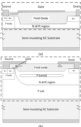
[image:3.612.352.521.55.318.2]Fig. 2 shows two simulated LDMOS embodiments estab-lished in distinct technologies: SOI and PN RESURF. 6H–SiC is used as the substrate material. In each transistor, the part enclosed by a box is transferred from the design developed by Arnold et al. [19] or Disney et al. [20]. These require either a thin (1.5 μm) or thick (16 μm) Si layer on a SiC wafer, both of which have already been demonstrated in [18] and [21]. The Si/SiC LDMOS with the SOI layout has a thinned-down region 0.2-μm-thick, according to [19], [22]. For fair comparison, they have the same channel dimensions,
Fig. 2. Layout of the simulated(a)SOI-like and(b)bulk-Si-like Si/SiC power LDMOS with about 600-V breakdown voltage.
SiC substrate (300 μm) and drift region length (∼44 μm). These lead to very similar threshold voltages (∼2 V at 300 K) and breakdown voltages of about 640 V.
The use of SI SiC reduces the thermal resistance of both devices, allowing them to approach the heat transfer ability of SiC-based counterparts [23]. A second benefit can be radiation hardening as in SOS and SOD [24], but this need to be qualified by systematic experiments. Third, vertical leakage is minimized, as the SOI layout does, making high-temperature operating possible. However, substrate-assisted depletion (SAD) is suppressed, due to the fact that no dopant in the SiC substrate can create the back-RESURF effect [15], [25] that are inherent in SOI and bulk-Si case. This vertical depletion can be positive or negative to devices’ figure of merit, which depends on the RESURF dimension (2-D or 3-D). In the transistors shown inFig. 2, this aspect is desirable, and therefore the layout in the Si region should be able to facilitate self-depletion, to compensate for the weak SAD in the Si/SiC architecture.
Similar to SOI wafers, charge exists along the Si/SiC interface due to the termination of the crystal structure of both materials. This additional charge may raise leakage current significantly and the RESURF condition can be distorted. For instance, the presence of a Si/poly-Si/poly-SiC interface could be the reason why the Si/SiC LDMOSFET conducts reverse current one order magnitude higher than that of the SOI counterpart [16]. Although Sasada et al. [21] reported that their Si/SiC samples have negative surface charge of less than 2×1010cm−2(similar to+4×1010cm−2for the Si/SiO2[19]),
large leakage is still able to be produced if the Si layer is N-type and has very low doping (Nd=1×1013 cm−3) [21]. Conversely, the Si/SiC wafers with P-type silicon exhibits leakage lower than that of the bulk-Si reference [21], indi-cating that the bonded substrate has a device-quality Si layer with good electrical insulation properties, and that the leakage is likely to be induced by the depletion or inversion in the very low-doped N-type region [21]. This phenomenon may affect the electrical characteristics of the two transistors in Fig. 2
differently as they are designed on a Si region with opposite doping types. Recent TEM results [18] show that a very sharp interface and thin amorphous layer (<5 nm) are visible in the majority of our Si/SiC bonded wafers, but in some areas an island-like defect is formed and extends up to 8 nm of the Si side [see Fig. 1(b)], which potentially contributes more interfacial charges. In this simulation, the interface effect is simplified by setting the surface charges of Si/SiO2 and
Si/SiC to +4×1010 cm−2 [19] and −2×1010 cm−2 [21], respectively. It is worth noting that this Si/SiC interface charge will vary according to the wafer bonding process and subsequent annealing, which will affect device performance.
III. SIMULATIONSETUP
Device simulation is carried out using SILVACO ATLAS, for the two Si/SiC transistors and their SOI and bulk-Si equivalents. As described in Section II, interface charges are defined along the Si/SiO2 and Si/SiC surface, namely +4×1010cm−2 [19] and−2×1010 cm−2[21], respectively. Carrier lifetimes are set to 1.5 and 70μs at room temperature for the thin and thick-film structures, to achieve generation lifetimes, which are similar to those in [19]. The influence of temperature and doping density on carrier lifetime and mobility are considered with the physical-based analytical models developed by Klaassen [29], [30] according to [19]. These models have been used in [26] to benchmark the thin-film Si/SiC transistor to the SOI device developed by Arnold et al. [19].
IV. SIMULATIONRESULTS
A. OFF-State Performance
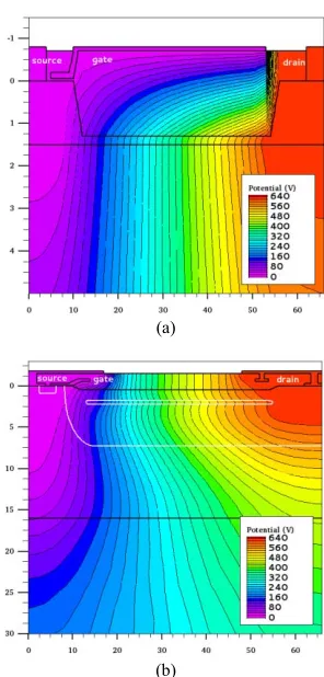
[image:4.612.362.510.52.361.2]1) Potential Distribution:Fig. 3shows the potential contour of the two transistors at the onset of breakdown (640 V), with the substrate contact connected to ground. A nearly linear voltage drop can be seen along the x -direction of the drift region of each device, which results from the vertical depletion induced by the SOI layout or P-N pairs. The gate
Fig. 3. Potential distribution at 640 V for (a) SOI-like and (b)bulk-Si-like Si/SiC power LDMOS (axes unit: µm). Their substrate contacts are grounded.
contact covers most parts of the field oxide (FOX) in the thin-film Si/SiC LDMOS, creating a SOI RESURF that distributes the electric field evenly. The blocking voltage in this case is governed in part by the thickness of the FOX, which resembles the criteria for the BOX in the traditional SOI structures [22]. Furthermore, negligible interface effects on the potential gra-dient are observed, owing to the charge density specified along the Si/SiC surface being far lower than that of the drift region. In the thick-film Si/SiC transistor, the depletion mechanism is similar to the conventional design [20], except for the voltage being supported vertically by the N drift/P-sub/SiC structure rather than the N drift/P-sub junction alone.
3716 IEEE TRANSACTIONS ON ELECTRON DEVICES, VOL. 64, NO. 9, SEPTEMBER 2017
Fig. 4. Temperature dependence of leakage current for the SOI, bulk-Si, SOI Si/SiC and bulk-Si Si/SiC LDMOS at a drain voltage of 300 V, along with two lines (∝ni&∝n2i) representing generation and diffusion component, respectively.
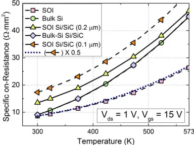
Fig. 5. Temperature dependence of low-side specific on-resistance for the SOI, bulk-Si, bulk-Si Si/SiC, and two SOI Si/SiC transis tors that have differing Si layer thickness, namely 0.2 and 0.1µm. The dotted line is derived from halving the curve for the SOI Si/SiC LDMOS with a 0.1-µm-thick Si film.
higher carrier lifetime [19]. The gradients of their leakages against temperature are similar and can be mostly described by the ∝ni line (seeFig. 4). However, the bulk-Si LDMOS distinguishes itself from the others by having a much larger leakage current, whose increase rate approaches that of the ∝n2i line. The reason for this is that the generation leakage is raised when the depletion region expands into the P-type substrate of the bulk-Si transistor, and that a vertical diffusion current appears owing to the absence of electrical isolation.
B. ON-State Performance
1) Low-Side SpecificON-Resistance:The effect of tempera-ture on the low-side specific on-resistance of different devices can be seen inFig. 5. The bias conditions of Vds=1 V and Vgs = 15 V are applied in the simulation to minimize the
influence of channel resistance and “pinch-off,” thus the total resistance mainly depends on the quantity of donors in the drift region. All the transistors are designed with an effective dose [32] of around 3×1012 cm−2 [20], [26] in their drift regions for 600 V, except for the Philips’ LDMOS having about 6×1012 cm−2 on account of the
polysilicon-Oxide-siliCon-Oxide-Silicon structure [28]. It is worth noting that in the SOI and SOI-like Si/SiC device, a charge-rich region will be formed underneath the FOX because of the gate extension and applied gate bias [28]. However, the effect of such induced electrons on the resistance is limited and not as substantial as that shown in [32], where one third of the drift region is flooded with accumulation carriers, accounting for 68% of the total current conduction [32].
Under this setting, very high charge density (cm−3) is present in the SOI group and their carrier transports are dominated by impurity scattering [19], [29], [30]. By contrast, the thick-film (16 μm) transistors in JI technology accom-modate far less impurity atoms per unit volume and hence lattice scattering prevails [19], [29], [30]. This brings about the on-resistance of the SOI-like Si/SiC transistors less sensitive to temperature compared with the thick-film Si/SiC counterpart, but in return a lower conductivity is observed, with the 0.1-μm-thick device having the least conductance due to the highest impurity concentration (see Fig. 5). No difference in the resistance is observed between the bulk-Si and its equivalent Si/SiC device, because the p-sub region in this Si/SiC plays the same role as the one in the traditional bulk-Si structure, facilitating a back-RESURF for the drift region. However, the thin-film SOI exhibits a resistance slightly lower than those of the two bulk-Si LDMOSFETs at room tempera-ture. Its degradation rate with temperature is also smaller than those of any other structures. This is because the transistor features a double SOI RESURF effect, and can be regarded as two SOI devices with a 0.1-μm Si layer working back-to-back [28], as can be demonstrated with the dotted line in Fig. 4, which is obtained from halving the results of the 0.1-μm Si/SiC, which operates with just a single SOI RESURF technique.
As opposed to the SOI, the thin and thick-film Si/SiC tran-sistors have 56% and 5% more low-side resistance at 300 K, respectively, increasing to 79% and 71% at 573 K. Therefore, it is advantageous in high-temperature operations that high doping density and high-order RESURF are employed in the unipolar transistors. In the case of the Si/SiC architecture, the 3-D super-junction layout [33] could be the answer to the improvement of the on-resistance, as the SAD effect is weak in the Si-on-(SI) SiC structure such that the depletion of the of 3-D RESURF structure is mainly induced from the sides, in the direction of device width, leading to a double RESURF effect with relatively high doping.
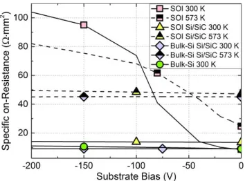
2) High-Side Specific ON-Resistance: Fig. 6 demonstrates the high-side specific on-resistance as a function of substrate voltage for the simulated transistors at ambient tempera-tures of 300 and 573 K. The gate and drain terminals are biased at 15 and 1 V, with the substrate voltage varying from 0 to −200 V. In order to reduce the effect of substrate bias on the backgate (P body), the N-drift region in the bulk-Si structure is extended laterally to enclose the channel region [34]. Furthermore, this LDMOS is excluded from the simulation at 573 K, owing to the activation of parasitic bipolar junction transistors that distort the device’s characteristics.
[image:5.612.78.270.277.421.2]Fig. 6. Relationships between specific on-resistance and substrate bias for the simulated LDMOSFETs at 300 and 573 K, excluding the one for the bulk-Si at 573 K.
ambient temperature, so does the bulk-Si at 300 K. The common reason is that they all have a high-resistive substrate, which sustains most of the applied voltage, thereby reducing the depletion in the Si active region [34]. In the bulk-Si and its equivalent Si/SiC device, the thick Si layer (16 μm) and application of charge compensation (triple RESURF) [35] also alleviate the effect of substrate bias, by increasing the deple-tion limit and decreasing the depledeple-tion width, respectively. However, in the SOI device, potential is confined by the BOX so that the depletion in the top Si film is enhanced. This significantly lessens the effective area for current conduction in the already-thin Si layer, resulting in a rapid rise of on-resistance up to−100 V at 300 K (seeFig. 6). Beyond this value, the expansion of depletion region with the substrate bias is hindered by the formation of an inversion layer [35], leading to a less drastic increase in on-resistance. Similar features are observed in the curve for the SOI at 573 K, but the impact of substrate bias seems to be weakened, yielding an even less abrupt change and eventually the resistance is lower than that at 300 K. This is because with the presence of large amount of thermally generated carriers, the depletion region does not function as strong a potential barrier as at 300 K.
Despite reducing low-side resistance as shown in the previ-ous section, the SAD effect in this case is disrupted by the substrate bias, thereby increasing the resistance. Compared with the SOI, the equivalent Si/SiC achieves 86% and 40% reduction in the high-side resistance at 300 and 573 K, respectively, under a substrate potential of −200 V. Likewise, the bulk-Si Si/SiC has 91% and 36% lower high-side resistance at 300 and 573 K. By introducing a step Si film on a thicker BOX layer [36], this downside in the SOI can be partially resolved but the dependence on substrate bias still exists, which gives rise to a difference between low- and high-side resistances.
C. Transient Self-Heating
The setup used in this section, for assessing the effects of self-heating, is a rectangle power pulse (RPP), which has been proven to be equivalent to the clamp inductive switching [37]. Applications of this approach for LDMOS devices can be found in [2], [3], [37]. All the simulated transistors are simulated in this section as being 1-mm-wide and have a 300-μm thick substrate, under which a thermal contact is
Fig. 7. Dynamic temperature responses to a 90 W/mm2power pulse 10-µs-long under a RPP setup, for the simulated structures.
defined and fixed at 300 K. A dc gate voltage of 15 V is applied and the drain biased by a pulse voltage source that lasts 10μs, with its value tailored for each device to achieve the same power pulse of 90 W/mm2. This value [2] is selected to energise the device and does not represent normal power dissipations [2].
Due to strong self-heating, the power applied in the SOI drops from the initial value to about 67 W/mm2 at 10 μs, and the maximum temperature rises up to 550 K (seeFig. 7). On the contrary, other devices have far less temperature increases and their power pulses are nearly the same. The disparity of junction temperature between the bulk-Si and its equivalent Si/SiC starts to appear at 2.5 μs, indicating the cooling effect of the SiC substrate. The thin-film Si/SiC also receives such thermal benefit, but a slightly rapider temper-ature rise is found when compared with the bulk-Si devices, mainly due to a nonuniform heating [38] caused by the linear doping in the drift region. Nevertheless, the maximum junction temperature of this device is the same as that of the bulk-Si (green) at 10 μs, and thereafter decays faster than that of the thick-film Si/SiC counterpart. One can expect that more thermal improvement can be offered by the Si/SiC solutions under conditions where longer and larger power pulses are present.
V. CONCLUSION
[image:6.612.323.553.56.195.2]3718 IEEE TRANSACTIONS ON ELECTRON DEVICES, VOL. 64, NO. 9, SEPTEMBER 2017
low-side -resistance 5% and 71% higher than the SOI at 300 and 573 K, respectively, which is caused by lower doping density in the drift region. Under high-side conditions, the resistance of the SOI increases with the substrate potential, and eventually reaches a value 86% and 91% greater than those of the SOI Si/SiC and bulk-Si Si/SiC, respectively, at−200 V and 300 K. At 573 K, these differences are reduced to 40% and 36% correspondingly. In addition, their transient self-heating effects are evaluated via a RPP circuit, showing that the Si/SiC structures have thermal behaviors comparable to the bulk-Si with a 10μs pulse of 90 W/mm2. Coupled with the insulation property of SiC substrates, this remarkable cooling ability makes the Si/SiC a potential solution for high temperature and power applications.
REFERENCES
[1] V. Khemka, V. Parthasarathy, Z. Ronghua, A. Bose, and T. Roggenbauer, “Detection and optimization of temperature distribution across large-area power MOSFETs to improve energy capability,” IEEE Trans. Electron Devices, vol. 51, no. 6, pp. 1025–1032, Jun. 2004.
[2] E. Arnold, H. Pein, and S. P. Herko, “Comparison of self-heating effects in bulk-silicon and SOI high-voltage devices,” in IEDM Tech. Dig., San Francisco, CA, USA, Dec. 1994, pp. 813–816.
[3] H. T. Lim, F. Udrea, D. M. Garner, and W. I. Milne, “Modelling of self-heating effect in thin SOI and Partial SOI LDMOS power devices,” Solid-State Electron., vol. 43, no. 7, pp. 1267–1280, 1999.
[4] J. Roig, D. Flores, S. Hidalgo, M. Vellvehi, J. Rebollo, and J. Millan, “Study of novel techniques for reducing self-heating effects in SOI power LDMOS,” Solid-State Electron., vol. 46, no. 12, pp. 2123–2133, 2002.
[5] S. D. Hu, X. R. Luo, B. Zhang, and Z. J. Li, “Design of compound buried layer SOI high voltage device with double windows,” Electron. Lett., vol. 46, no. 1, pp. 82–84, Jan. 2010.
[6] P. Baine et al., “Improved thermal performance of SOI using a com-pound buried layer,” IEEE Trans. Electron Devices, vol. 61, no. 6, pp. 1999–2006, Jun. 2014.
[7] J. Roig, D. Flores, I. Cortes, S. Hidalgo, and J. Millan, “Thin film SOI and SOS LDMOS structures with linear doping profile and enlarged field plate,” in Proc. 24th Int. Conf. Microelectron., vol. 1. May 2004, pp. 141–144.
[8] Z. An, C. Men, X. Xie, M. Zhang, P. K. Chu, and C. Lin, “Fabrication of silicon-on-AlN novel structure and its residual strain characterization,” J. Cryst. Growth, vol. 244, no. 1, pp. 27–32, 2002.
[9] B. A. Biegel, M. A. Osman, and Z. Yu, “Analysis of aluminum-nitride SOI for high-temperature electronics,” in Proc. HiTEC, Jan. 2000, pp. 1–8. [Online]. Available: http://people.nas.nasa.gov/~biegel/ pubs/hitec_paper.pdf
[10] A. Aleksova et al., “Silicon-on-diamond: An advanced silicon-on-insulator technology,” Diamond Rel. Mater., vol. 14, pp. 308–313, Mar./Jul. 2005.
[11] S. Duangchan et al., “The silicon on diamond structure by low-temperature bonding technique,” in Proc. Electron. Compon. Technol. Conf. (ECTC), May 2015, pp. 187–192.
[12] M. Rabarot et al., “Silicon-on-diamond layer integration by wafer bonding technology,” Diamond Rel. Mater., vol. 19, nos. 7–9, pp. 796–805, 2010.
[13] P. M. Gammon, “Silicon and the wide bandgap semiconductors, shaping the future power electronic device market,” in Proc. ULIS Conf., Coventry, U.K., Mar. 2013, pp. 9–13.
[14] S. Arulkumaran, T. Egawa, H. Ishikawa, and T. Jimbo, “High-temperature effects of AlGaN/GaN high-electron-mobility transistors on sapphire and semi-insulating SiC substrates,” Appl. Phys. Lett., vol. 80, pp. 2186–2188, Mar. 2002.
[15] C.-F. Huang et al., “3510-V 390-m·cm24H-SiC lateral JFET on a semi-insulating substrate,” IEEE Electron Device Lett., vol. 30, no. 9, pp. 957–959, Oct. 2009.
[16] S. Lotfi, L.-G. Li, Ö. Vallin, L. Vestling, H. Norström, and J. Olsson, “LDMOS-transistors on semi-insulating silicon-on-polycrystalline-silicon carbide substrates for improved RF and thermal properties,” Solid-State Electron., vol. 70, pp. 14–19, Apr. 2012.
[17] H. Shinohara, H. Kinoshita, and M. Yoshimoto, “Si metal-oxide-semiconductor field-effect transistor on Si-on-SiC directly bonded wafers with high thermal conductance,” Appl. Phys. Lett., vol. 93, no. 12, p. 122110, 2008.
[18] P. M. Gammon et al., “The effect of interfacial charge on the develop-ment of wafer bonded silicon-on-silicon-carbide power devices,” Mater. Sci. Forum, vol. 897, pp. 747–750, May 2017.
[19] E. Arnold, T. Letavic, S. Merchant, and H. Bhimnathwala, “High-temperature performance of SOI and bulk-silicon RESURF LDMOS transistors,” in Proc. ISPSD, May 1996, pp. 93–96.
[20] D. R. Disney, A. K. Paul, M. Darwish, R. Basecki, and V. Rumennik, “A new 800 V lateral MOSFET with dual conduction paths,” in Proc. ISPSD, Jun. 2001, pp. 399–402.
[21] Y. Sasada, T. Kurumi, H. Shimizu, H. Kinoshita, and M. Yoshimoto, “Junction formation via direct bonding of Si and 6H-SiC,” Mater. Sci. Forum, vols. 778–780, pp. 714–717, Feb. 2014.
[22] S. Merchant, E. Arnold, H. Baumgart, S. Mukherjee, H. Pein, and R. Pinker, “Realization of high breakdown voltage (>700 V) in thin SOI devices,” in Proc. ISPSD, Apr. 1991, pp. 31–35.
[23] C. W. Chan et al., “Simulations of a lateral PiN diode on Si/SiC substrate for high temperature applications,” Mater. Sci. Forum, vols. 821–823, pp. 624–627, Jun. 2015.
[24] N. K. Annamalai and J. Chapski, “Novel dielectrics for SOI structures,” in Proc. SOS/SOI Technol. Conf., Key West, FL, USA, Oct. 1990, pp. 59–60.
[25] W.-S. Lee et al., “Design and fabrication of 4H-SiC lateral high-voltage devices on a semi-insulating substrate,” IEEE Trans. Electron Devices, vol. 59, no. 3, pp. 754–760, Mar. 2012.
[26] C. W. Chan, P. A. Mawby, and P. M. Gammon, “Analysis of linear-doped Si/SiC power LDMOSFETs based on device simulation,” IEEE Trans. Electron Devices, vol. 63, no. 6, pp. 2442–2448, Jun. 2016. [27] C. W. Chan, Y. Bonyadi, P. A. Mawby, and P. M. Gammon, “Si/SiC
substrates for the implementation of linear-doped power LDMOS studied with device simulation,” Mater. Sci. Forum, vol. 858, pp. 844–847, May 2016.
[28] T. Letavic et al., “High performance 600 V smart power technology based on thin layer silicon-on-insulator,” in Proc. ISPSD, May 1997, pp. 49–52.
[29] D. B. M. Klaassen, “A unified mobility model for device simulation— I. Model equations and concentration dependence,” Solid-State Electron., vol. 35, no. 7, pp. 953–959, 1992.
[30] D. B. M. Klaassen, “A unified mobility model for device simulation— II. Temperature dependence of carrier mobility and lifetime,” Solid-State Electron., vol. 35, no. 7, pp. 961–967, 1992.
[31] S. Merchant, E. Arnold, and M. Simpson, “Tunneling in thin SOI high voltage devices,” in Proc. ISPSD, May 1995, pp. 130–135.
[32] J. Wei et al., “High-voltage thin-SOI LDMOS with ultralow ON-resistance and even temperature characteristic,” IEEE Trans. Electron Devices, vol. 63, no. 4, pp. 1637–1643, Apr. 2016.
[33] F. Udrea, A. Popescu, and W. I. Milne, “A new class of lateral power devices for HVICs based on the 3D RESURF concept,” in Proc. Bipolar/BiCMOS Circuits Technol. Meet., Minneapolis, MN, USA, Sep. 1998, pp. 187–190.
[34] A. W. Ludikhuize, “A versatile 700-1200-V IC process for analog and switching applications,” IEEE Trans. Electron Devices, vol. 38, no. 7, pp. 1582–1589, Jul. 1991.
[35] E. Arnold, S. Merchant, M. Amato, S. Mukherjee, H. Pein, and M. A. Ludikhuize, “Comparison of junction-isolated and SOI high-voltage devices operating in the source-follower mode,” in Proc. ISPSD, May 1992, pp. 242–243.
[36] T. Letavic et al., “600 V power conversion system-on-a-chip based on thin layer silicon-on-insulator,” in Proc. ISPSD, May 1999, pp. 325–328. [37] G. Van den bosch, P. Moens, P. Gassot, D. Wojciechowski, and G. Groeseneken, “Analysis and application of energy capability char-acterization methods in power MOSFETs,” in Proc. Solid-State Device Res. Conf. (ESSDERC), Sep. 2004, pp. 453–456.
[38] Y.-K. Leung et al., “Spatial temperature profiles due to nonuniform self-heating in LDMOSs in thin SOI,” IEEE Electron Device Lett., vol. 18, no. 1, pp. 13–15, Jan. 1997.