warwick.ac.uk/lib-publications
Manuscript version: Author’s Accepted Manuscript
The version presented in WRAP is the author’s accepted manuscript and may differ from the
published version or Version of Record.
Persistent WRAP URL:
http://wrap.warwick.ac.uk/107518
How to cite:
Please refer to published version for the most recent bibliographic citation information.
If a published version is known of, the repository item page linked to above, will contain
details on accessing it.
Copyright and reuse:
The Warwick Research Archive Portal (WRAP) makes this work by researchers of the
University of Warwick available open access under the following conditions.
Copyright © and all moral rights to the version of the paper presented here belong to the
individual author(s) and/or other copyright owners. To the extent reasonable and
practicable the material made available in WRAP has been checked for eligibility before
being made available.
Copies of full items can be used for personal research or study, educational, or not-for-profit
purposes without prior permission or charge. Provided that the authors, title and full
bibliographic details are credited, a hyperlink and/or URL is given for the original metadata
page and the content is not changed in any way.
Publisher’s statement:
Please refer to the repository item page, publisher’s statement section, for further
information.
Abstract— The equivalent circuit admittance of a lumped element
periodically loaded electrically dense array of slots at a material interface is derived for both, parallel and perpendicular, polarizations. The derivation is based on the methodology of Casey for deriving the equivalent circuit impedance of an unloaded wire mesh at a dielectric interface using the Wait-Hill formulation. Using the derived equivalent circuit admittance, a Booker type relation for unloaded wire grid and slot arrays, at general isotropic media interfaces, is obtained.
Index Terms— slot arrays, equivalent circuits, electromagnetic
scattering by periodic structures
I. INTRODUCTION
STARTING from the Wait and Hill formulation [1], which is a method of moments (MoM) formulation, Casey proposed in [2] a methodology for deriving simple, closed-form, expressions for the equivalent circuit impedance of an electrically dense (period significantly smaller than the wavelength), dielectric-backed, unloaded wire mesh screen for both polarizations, parallel and perpendicular. An analogous derivation of simple, closed-form, expressions for the admittance of an electrically dense orthogonal array of slots (patches), at a material interface (which is also loaded with lumped elements, Fig. 1) to the best of the authors’ knowledge, does not exist (and it is the subject of this paper). However, simple closed-form equivalent circuit impedance expressions for the unloaded array of slots on an air-dielectric interface were obtained, for both polarizations, in [3]. These expressions in [3] were obtained by combining the impedance of the wire grid on a dielectric substrate and a Booker type equation [4] in terms of the effective impedance (see (7) of [3] and [5],[6]). The wire grid impedance was obtained by a heuristic extension of Kontorovich’s average boundary conditions (BC), (1)-(2) in [3], using the effective permittivity expression (3) of [3]. Reference [7] highlights limitations of the method used in [3] to obtain simple, closed-form patch array formulae. For example, the lack of a description or explanation of polarization decoupling and azimuthal independence of the obtained equivalent circuit impedance expression. Hence, [7] adapts Casey’s assumption, (35) in [8], to the magnetic current and uses it as a starting approximation of their MoM derivation. Indeed, in [7], an analytical expression for the patch array equivalent circuit reactance is obtained, providing polarization and azimuthal angle description. However, [7] does not consider a material interface and lumped element loading. Furthermore, the derived analytical expression in [7] is not as simple as that of [3] since it contains an infinite sum, see (22) of [7]. Hence, the aim of the current paper is to derive a simple, closed-form, expression for the
Manuscript received August 30, 2015
C. Mias is with the University of Warwick, Coventry, CV4 7AL, United Kingdom, (e-mail: [email protected]; phone: 00442476522343; fax: 00442476418922).
[image:2.595.338.521.192.363.2]A. Freni is with the Department of Information Engineering, University of Florence, I-50139 Firenze, Italy.
Fig. 1. Geometry of the loaded slot array.
admittance of an electrically dense, lumped element loaded, slot array at a general isotropic media interface (Fig. 1) by avoiding the limitations of the methodology in [3]: (i) the use of a heuristic extension; (ii) the use of a Booker type equation limited to dielectric materials (i.e. µr(i) = µr(i+1) = 1 in Fig. 1) and (iii) the angle of
incidence limitation (see paragraph above (5) of [3]). Our derivation includes a novel Wait-Hill magnetic current formulation, shown in (10)-(11), for plane wave scattering from a lumped element loaded patch array at a general media interface (which is an extension of the free space magnetic current formulation in [9]) and subsequently applies the magnetic current approximation of [7]. Thus, our approach is related to the unloaded wire grid mesh approach and electric current approximation of Casey [2] and the free-space wire grid equivalent impedance derivation in [8] (with the loading applied as proposed in [10]) but here a loaded slot array is considered instead. In section III, using the derived equivalent circuit admittance, a Booker type relation for unloaded wire grid and slot arrays is obtained, that extends the Booker type relation for dielectric media, used in [3], to the case of general isotropic media. The benefits of deriving simple equivalent circuit expressions for electrically dense arrays are highlighted in [2],[3],[7],[11] (and papers citing them) and include physical insight and fast computation of the electromagnetic (EM) behavior of periodic structures in a variety of applications, such as EM shielding and absorption, frequency selective surface (FSS) radomes and artificial dielectrics. The more electrically dense is an array, the greater is the evanescence of the high order harmonics. This allows the use of simple transmission line models [3] to model single or multi-layer periodic structures [12].
II. DERIVATION OF THE WAIT-HILL FORMULATION
In this section a novel Wait-Hill formulation is derived for the solution of the problem depicted in Fig. 1. The worked-out plane wave transmission coefficient expression will be the starting point for calculating the desired analytical admittance expression for an
Simple admittance expression derivation of an electrically dense loaded slot array at a
material interface
electrically dense array, in Section III. The formulation requires a definition of the boundary condition (BC) - see (2) - at the two orthogonal slots of the reference unit cell (defined below). The BC (shown in [13] for a lossy dielectric window, and in [14] for an unloaded array) is in terms of the incident and scattered magnetic fields, the magnetic current, and the admittance per unit length as the slots are loaded with lumped elements (Fig. 1). The field notations used in [14] are employed here. The periodic part of the magnetic current is expressed as the sum of a periodic sawtooth function (to account for a sharp magnetic current discontinuity at the slot junction) with a harmonic function summation (9). By expressing the sawtooth function as a Fourier series, and substituting the resulting magnetic current expression into the BC ([1], [8] show the procedure), leads to simultaneous equations, (10) and (11). The use of the periodic sawtooth function and of the Kummer’s transformation of a series in the simultaneous equations allows us to obtain the desired analytic admittance expression when the array period is electrically small. This is done in Section III where only three unknowns are retained of the Fourier series expression of the magnetic current. The geometry of the periodic structure under consideration is shown in Fig. 1. The media on either side of the array are assumed to be lossy with permittivity ε(ν) = ε0εr(ν),
permeability µ(ν) = µ0µr(ν), conductivity σ(ν), intrinsic impedance η(ν)
and wavenumber kr(ν); where ν = i or i+1. The array coincides with
the y = 0 plane. The incident magnetic field ϑHinc, with amplitude H 0,
is assumed to be either parallel ( ϑ = || ) or perpendicularly ( ϑ = ⊥ ) polarized and it is given by
( ) ( )ˆ
0 ˆ00( )
( ) jkr i i inc
i
H e− +•
ϑH R = s Rϑn + (1) where ŝ(i)± = sx(i)x̂ ± sy(i)ŷ +sz(i)ẑ is the direction vector and
R = xx̂ + yŷ +zẑ. The polarization unit vector ϑn̂00(i)+, shown in Fig. 1, is defined in (4.55)-(4.56) of [14]. In the reference unit cell (|x| ≤Dx/2, |z| ≤Dz/2) of Fig. 1, the slot axes coincide with the z-axis
for reference slot A (xA = 0) and with the x-axis for reference slot B
(zB = 0). The BC
1
ν mod
(ν) (ν) ˆ ( )
[2 ( 1) ( )] ( ) ( )
i
inc i sctot sctot
A B L K
i
Y u M u
+ ϑ
=
+
∑
− + • = −H H H u
ν
(2) is imposed on each slot. In (2), which is an adaptation of the lossy dielectric window BC in [13], ‘mod’ is the modulo operator, i.e. (ν mod i) is zero for ν = i and one for ν = i+1. In addition, û =ẑ for slot A and û = x̂ for slot B. The BC is imposed at Rb by using, as in
[14] and [15], the equivalence between the narrow slot width, w, and the ‘wire’ radius, b, i.e. b=w/4. Thus, for slot A, Rb(x,y,z) = R(0,±b,z)
and for slot B, Rb(x,y,z) = R(x,±b,0); the sign ‘−’ corresponds to ν = i
and the sign ‘+’ corresponds to ν = i+1. Over the reference unit cell of Fig. 1, the per unit length load admittance is YL(K)(u) = Yυ(K) /l for
(Du−l)/2 ≤ |u| ≤Du/2 and zero otherwise; where K=A, u=z for slot A
and K=B, u=x for slot B. Yυ(K) is the lumped element admittance (see
Fig. 1). Since YL(K)(u) is periodic,
∑
∞−∞ =
π −
=
n
D nu j K n K
L u Y e u
Y ( )( ) ( ) 2 / (3)
with Yn(K) = (Yυ(K)/Du)(−1)nsinc(nπl/Du). The equivalent magnetic
current along the reference slots A and B is given by (xA = zB = 0)
( ) ( ) 2 / ( ) ( )
( )
( ) jkr i u is u j pu Du jkr i u is u
K K p
p
M u M e K e e
∞
− − −
Π ϑ
=−∞
= =
∑
π(4)
MΠ(K) is the periodic part of the magnetic current, p=m for slot A and
p=q for slot B. In (2), based on the equivalence principle, the total scattered field in medium (ν) for each slot contains the radiated field from each slot and its reflection from a perfectly electric conducting plane. Thus, H(ν)sctotK =H(ν)(sc)K±+Href sc(ν)K(±); the signs ‘−’ and ‘+’ correspond to ν = i and ν = i+1, respectively. For slot A, the magnetic current is assumed [14] to be in the negative z-direction in medium
ν = i and in the positive z-direction in medium ν = i+1, hence
(ν)ˆ (ν)
ν mod
( )
(ν)
(ν) (ν)
(ν) (ν) || (ν) || (ν)
( 1) 2
ˆ ˆ
( )
r mq
jk i
sc
m A
x m q mqy
mqz mq mqz mq
e A
D r
n n
±
− •
∞ ∞ ϑ ±
=−∞ =−∞
⊥ ⊥ ± ±
− =
× +
∑ ∑
r RH
n n
η
(5)The expression for H(v)ref scA(±) is also given by (5). Similarly, for slot B, H(( )ν ±sc)B and H( )ref scν B(±) are given by (5) when the subscript x is substituted with z (and vice-versa) and ϑAm with ϑBq. Subscripts on
the right include the harmonic order, “m and/or q”, the Cartesian coordinate “x,y,z” for vector components, and the medium index which appears within round brackets. Polarization subscripts (⊥,||) appear on the left of a variable. The direction vector of the mqth
harmonic is defined as r̂mq(ν)± = rqx(ν)x̂ ± rmqy(ν)ŷ + rmz(ν)ẑ in medium ν
and its components can be obtained from (4.24), (5.3)-(5.5) of [14].
||,⊥nmqz(ν) is the z-component of the polarization unit vector ||,⊥n̂mq(ν)± of
the mqth harmonic in medium ν which is defined in (4.55)-(4.56) of
[14]. The subscripts ± on the right of variables correspond to the ± sign of the direction vector r̂mq(ν)± above. Starting from (2) and
following the methodology of [8], which includes Kummer’s transformation of a series to improve its convergence [1][8][10], leads to (2) of [9]. Similar to [9], the right hand side terms of (1)-(2) of [9] are given by ΞA = −ϑn00(i)z2H0 and ΞB = −ϑn00(i)x2H0 where it
is assumed that exp(±jkr(i)sy(i)b) ≈ 1. However, in contrast with [9],
the coefficients of the left hand side terms are not related to those of the wire grid by the Booker equation shown in [9] because of the material interface. Instead, they are given as follows (it is assumed that 1+ exp(2jkr(ν)rmqy(ν)b) ≈ 2)
( )
1 ( )
( ) ( )
( )
( ) ( ) || ( ) || ( )
( )
mq b
i m
q B
z i mq
mqx mqz mqx mqz
j e
P
D
n n n n
ν ν
ν ν
ν ν ν ν
ω
+ε
−Γ=
⊥ ⊥
= −
Γ
× +
∑
(6)(
)
0( )
1
2 2
( ) 0( ) 0 ( ) || 0 ( )
0( )
( )
2 / 2
( ) ( )
ˆ ( )
ln 1 [1 ]
m
x
b i
m A A m z m z
m i
b D x
mz m
x e
Y Y n n
j D
e r
D −Γ
+
⊥ =
−
= + +
Γ
− − − + ∆
∑
ν ν νν ν
ν π
ν ν
ωε π
(7)
with
2 | | ( )
2 2 2
( ) ( ) || ( ) 2 | | ( )
( )
(
)
[1
]
'
q b D
mq x
x
b
m mqz mqz q mz
mq
q D
e
e
n
n
r
π
ν −
−Γ ∞
ν ⊥ ν ν π ν
ν =−∞
∆
=
+
−
−
Γ
Σ
(8) where the propagation constant Γmq is defined in (17) of [8]. The
[image:3.595.303.551.492.678.2]step ∆ at the slot “junction” is used to improve the convergence of the results. As stated in [9], the implementation of f∆ parallels that of [8]. Hence, starting from the f∆ expression in (21) of [8], the periodic part of the magnetic current is expressed as
2 /
( )K ( ) ( ) 'p j pu Du
p
M u f u K e
∞
− π
Π ∆ ϑ
=−∞
= ϕ +
∑
(9)where ϕ = 1 for slot A and ϕ = −1 for slot B. The magnetic current harmonic amplitudes ϑKp are expressed in terms of the amplitudes
ϑK'p as shown in (23) of [8]. Substituting (9) in (1) and (2) of [9]
leads to the following equation pair
( )
( ) ( ) ( )
0
ˆ '
'
' m 'm A m n A m n q B q
n q
m m A
Y A Y A P B
U
∞ ∞
ϑ ϑ − ϑ
=−∞ =−∞
+ −
+ ∆ = δ Ξ
∑
Σ
(10)( ) ( ) ( ) ( ) 0 ˆ ' '
'
' qm q B q n B q n
m A
n m
q q B
P A Y B Y B
V
∞ ∞
ϑ ϑ ϑ −
=−∞ =−∞
− + +
− ∆ = δ Ξ
∑
Σ
(11)
where ΞA = −||,⊥n00z2H0exp(−jkrsyb), ΞB = −||,⊥n00x2H0exp(−jkrsyb), and δm0, δq0 are Kronecker delta functions. Um is given by
( )0 0 ( ) ( ) 0 ( ) ( ) (1 ) (1 ) ˆ
2 2 ( )
(1 )
2
'
m nm
m m A n A
n
q m
q B q
U Y j Y j
m m n
P j q ∞ − =−∞ ∞ =−∞ − δ − δ = +
π π −
− δ + π
∑
Σ
(12)Vq is given by the right hand side of (12) if subscripts and
superscripts m0, m(A), (m), q(B), (A), (B), (m−n)0 are replaced by 0q, q(B), (q), m(A), (B), (A), 0(q−n), respectively, and series index q by index m. Denominator variables m and (m−n) should be replaced by q and (q−n).
As stated in [9], the extra equation needed for the unknown parameter ∆ is given by (28) of [8] where the expressions for Gm(A),
Gq(B) and W are also given. It is obtained from
) | | ( ) | | ( 0 0 2 1 0 0 2 1 + − + − ∂∂ = ∂∂ = ∂∂ = = ∂ ∂ + = + x x M x x M z z M z z
MA A B B
(13) which is the magnetic current dual version of (26) of [1].
III. EQUIVALENT CIRCUIT ADMITTANCE OF THE ELECTRICALLY DENSE ARRAY AND BOOKER TYPE RELATION
For the derivation of the equivalent circuit admittance of the slot array it is assumed that Dx = Dz = D. Furthermore, it is assumed that
the loading of the slots is everywhere the same, i.e. Y0(A) = Y0(B) = Y0.
The approximation
( )K ( ) 0 ( )
MΠ u ≈ϑK + ϕf∆ u (14) is made for an electrically small period. Hence, (10) (11) and (28) of [8] lead to the following reduced matrix equation,
(0)
0( ) 0( ) 0
0 0 00
(0)
0( ) 0 0 0 00
0( )
0( ) 0( )
ˆ 2 ˆ 2 0 A B z B x A A B
Y P U
A H n
P Y V B H n
G G W
ϑ ϑ ϑ ϑ − − − − = − − ∆ (15)
with G0(A) = jkr(ν)sz(ν), G0(B) = jkr(ν)sx(ν), W = 2/D; ν = i or i +1. In
addition, if λ/D is sufficiently large so that ∆m(ν) in (8) and ∆q(ν) can be
neglected, for m = 0 and q = 0, respectively, and for the approximations sx+λq/D≈ λq/D and sz+λm/D≈ λm/D to hold for q≠ 0 and m≠ 0, respectively, then the following expressions are
obtained for the terms in (15)
1
2 2
0( ) 0 ( ) ( ) ( ) ( )
ˆ i [(1 ) (1 ) ]
A z z
i
Y Y s ν Xν s ν ν
ν +
=
≈ +
∑
− + − Θ (16)1
2 2
0( ) 0 ( ) ( ) ( ) ( )
ˆ i [(1 ) (1 ) ]
B x x
i
Y Y s ν Xν s ν ν
ν +
=
≈ +
∑
− + − Θ (17)1
(0) (0)
( ) ( ) ( )
0( ) 0( )
i
x z
A B
i
P P s ν s ν ν
ν
+ =
= ≈
∑
Θ (18)1 ( )
0 ( )
( ) i z r i s j U X D k ν ν ν ν + = ≈
∑
, 1 ( )0 ( )
( ) i x r i s j V X D k ν ν ν ν + =
≈
∑
(19)where
(
b D)
e j
X( ) ( ) 1 −2π /
ν
ν =− ωεπ − ,
D sy( )
) ( ) ( 1 ν ν ν = η
Θ (20)
The transmission coefficient expression is used to obtain the equivalent circuit admittance expressions. Since only the fundamental (q = m = 0) harmonic propagates in electrically dense arrays, the co-polarized and cross-co-polarized transmission coefficients are given by
( ) * ( ) * *
( 1) * ( 1) 0
( ) ( )
( ) ( )
tran tran
i i w g
w out w out
w g inc inc
i i
g in g in
F E H T H E H
η
η
η
+η
+= R = R = −
R R
(21) assuming Rout= Rin= R(x, 0, z). The symbols g = ⊥,|| (g* = ||,⊥) and w = ⊥,|| (w* = ||,⊥) represent the incident electric (magnetic) field polarization and scattered electric (magnetic) field polarization, respectively, and
* 0 * 00 ( 1) * 0 * 00 ( 1)
* *
( 1) ( 1) ( 1) ( 1)
g w z i g w x i
w g
i y i x i y i z
A n B n
F
s D s D
η
η
+ +
+ + + +
= +
(22)
Solving (15) for A0 and B0 one can evaluate (22) and show that the
cross-polarization is zero. Furthermore, the co-polarized transmission coefficient for perpendicular (electric field) polarization is,
1
( ) ( )
1 1
( ) ( ) ( 1) ( 1)
2( / )
( / ) ( / )
i y i
s i y i i y i
s T
Y s s
η
η
η
− ⊥ ⊥ − − ⊥ + + =+ + (23)
where η(ν)/sy(ν) is the transmission line impedance and ⊥Ys is the
equivalent circuit admittance of the loaded slot array
(
)
1( )
2 / 2
0 ln 1 (1 ( ))
2 i b D s y i j D
Y Y D e π ν s ν
ν ε ω π + − ⊥ =
= − −
∑
+ (24)For parallel (electric field) polarization, the co-polarized transmission coefficient is
1 ( ) ( 1)
|| || 1 1
|| ( ) ( ) ( 1) ( 1)
2( )
( ) ( )
i y i
s i y i i y i
s T
Y s s
η
η
η
− + − − + + =+ + (25)
where η(ν)sy(ν) is the transmission line impedance and ||Ys is the
equivalent circuit admittance of the array
(
2 /)
|| 0 ln 1 ( ) ( 1)
b D
s i i
j D
Y Y D ω e π ε ε
π − +
= − − + (26)
In [16], based on the Wait-Hill formulation and [2], the equivalent circuit impedance of a periodically loaded wire grid at a material interface was obtained for perpendicular (electric field) polarization ([16], Eq. 17)
(
2 /)
( ) ( 1)0
( ) ( 1)
ln 1 b D i i
g
i i
j D
Z Z D ω e π µ µ
π µ µ
+ −
⊥
+
= − −
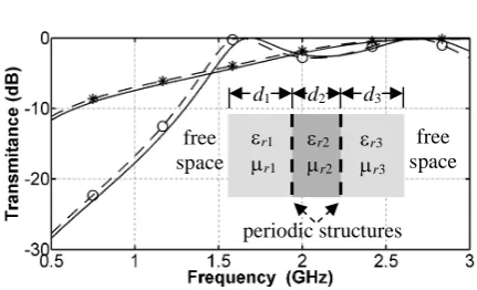
Fig. 2. Co-polarized transmittance results; T⊥ ⊥: () and T|| || : (). CST:
dashed line. Transmission line analysis using (24) and (26): Solid line. The CST cross-polarization results are less than −30 dB.
and parallel (electric field) polarization ([16], Eq. 18)
(
)
( ) 2 /
|| 0
2
( 1) ( ) ( )
( ) ( 1) ( ) ( 1)
ln 1
1
2
i b D
g
i y i i
i i i i
j D
Z Z D e
s
π
ωµ
π
µ
ε
µ
µ
ε
ε
−
+
+ +
= − −
−
× −
+ +
(28)
Ignoring the lumped elements and using Snell’s law of refraction it can be readily shown that
|| ( ) ( 1)
|| [ ( ) ( 1)][ ( ) ( 1)]
g g i i
s s i i i i
Z Z
Y Y
µ µ ε ε µ µ
⊥ +
⊥ = = + + + +
(29)
If media i and i+1 are (lossy) dielectrics (µ(i) = µ(i+1) = µ0) and the
angle of incidence is in the x-y or z-y plane, then (29) leads to (η0)2/(4ε
eff /ε0) with εeff = [ε(i) + ε(i+1)]/2 which are identical to (7) and
(3) of [3], if medium i is free space. It is worth noting that (29) extends the Booker type relation for dielectric media, used in [3], to the case of general isotropic media.
IV. NUMERICAL EXAMPLE
An arbitrary multilayer configuration, shown in Fig. 2, is used to compare the transmission line results of (24) and (26) to those of CST [17]. The periodic structures (defined in Fig. 1) are identical. The periods are Dx = Dz = D = 8 mm, the slot width is w = 4b = 0.4 mm,
the lumped element inductance value is L = 20 nH. The angles of incidence are ξ=70° and ψ=22.5°. The material layer values are:
εr1 =εr3 = 1.5, µr1 = µr3 = 1, εr2 = 3, µr2 = 2, d1 = d3 = 20 mm and
d2 = 12 mm. For the transmission line analysis, it is assumed that d2
is sufficiently large such that evanescent harmonic coupling between the two periodic structures can be neglected. There is a good agreement between the full wave CST and the equivalent circuit transmission line analysis results (Fig. 2). An advantage of using the transmission line model based on the approximate expressions (24) and (26) is that its results are computed much faster than those of the CST software as no linear system construction and solution (as it is the case for the CST) is required.
V. CONCLUSION
The admittance of the electrically dense lumped element loaded orthogonal slot array was derived based on the methodology of Casey. The derivation avoids the limitations of a previous methodology based on a Booker type equation and Kontorovich’s average boundary condition. In addition, a Booker type relation for unloaded wire grid and slot arrays, at general isotropic media interfaces, is obtained. As indicated in [15] the lumped elements may
be surface mount or in printed form. An example of loaded orthogonal slots is the slotted Jerusalem cross, where the region at the end caps may be considered as a printed form of a lumped element inductor. The developed analytic expression, see (24), indicates why the slotted Jerusalem cross is not an optimal frequency selective surface element (i.e. its admittance changes with frequency); an explanation is given in section 3.4 of [8] for a wire grid where a solution to the problem was suggested in the form of a lumped element inductor. Hence, for an orthogonal slot frequency selective surface, a lumped element capacitor in addition to the lumped element inductor is needed. Practical implementations of these lumped elements will be the subject of future work.
REFERENCES
[1] D.A. Hill and J.R. Wait, “Electromagnetic scattering of an arbitrary plane-wave by a wire mesh with bonded junctions,” Canadian Journal of Physics, vol. 54, no. 4, pp. 353-361, 1976.
[2] K.F. Casey, “Electromagnetic shielding by advanced composite materials,” Air Force Weapons Laboratory, Interaction Notes, C.E. Baum, Ed. Note 341, June 1977.
[3] O. Luukkonen, C. Simovski, G. Granet, G. Goussetis, D. Lioubtchenko, A.V. Raisanen, and. S.A. Tretyakov, “Simple and Accurate Analytical Model of Planar Grids and High-Impedance Surfaces Comprising Metal Strips or Patches,” IEEE Trans. Antennas Propag., vol. 56, no. 6, pp. 1624-1632, 2008.
[4] J. Moore, “Extension of the Babinet principle to scatterers with lumped impedance loads,” Electron. Lett., vol. 29, no. 3, pp. 301-302, 1993. [5] R. C. Compton, L. B. Whitbourn, and R. C. McPherdan, “Strip gratings
at a dielectric interface and application of Babinet’s principle,” Appl. Opt., vol. 23, no. 18, pp. 3236–3242, Sept. 1984.
[6] L. B. Whitbourn and R. C. Compton, “Equivalent-circuit formulas for metal grid reflectors at a dielectric boundary,” Appl. Opt., vol. 24, no. 2, pp. 217–220, 1985.
[7] D. Cavallo, W. H. Syed, and A. Neto, “Closed-form analysis of artificial dielectric layers—Part I: Properties of a single layer under plane wave incidence,” IEEE Trans. Antennas Propag., vol. 62, no. 12, pp. 6256– 6264, Dec. 2014.
[8] C. Mias and A. Freni, “Generalized Wait-Hill formulation analysis of lumped-element periodically-loaded orthogonal wire grid generic frequency selective surfaces”, Progress in Electromagnetics Research, vol. 143, pp. 47-66, 2013.
[9] C. Mias and A. Freni, “Magnetic current formulation for periodically loaded slots,” Electron. Lett., vol. 50, no. 16, pp. 1120-1121, 2014. [10] J.R. Wait, “On the theory of scattering from a periodically loaded wire
grid,” IEEE Trans. Antennas Propagat., vol. 25, no. 3, pp. 409-413, 1977.
[11] K.F. Casey, “Electromagnetic shielding behavior of wire-mesh screens,” IEEE Trans. Electromagn. Compat., vol. 30, no. 3, pp. 298-306, Aug. 1988.
[12] N. Behdad, and M. Al-Joumayly, “A generalized synthesis procedure for low-profile, frequency selective surfaces with odd-order bandpass responses,” IEEE Trans. Antennas Propag., vol. 58, no. 7, pp. 2460– 2464, July 2010.
[13] T. K. Sarkar, M. F. Costa, C.-L. I, and R. F. Harrington, “Electromagnetic transmission through mesh covered apertures and arrays of apertures in a conducting screen,” IEEE Trans. Antennas Propagat., vol. 32, no. 9, pp. 908–913, 1984.
[14] B.A. Munk, Frequency Selective Surfaces: Theory and design, John Wiley and Sons, 2000.
[15] J. P. Skinner and B. A. Munk, “Mutual coupling between parallel columns of periodic slots in a ground plane surrounded by dielectric slabs,” IEEE Trans. Antennas Propagat., vol. 40, pp. 1324–1335, 1992. [16] C. Mias, and A. Freni, “Wait–Hill MoM for a lumped element loaded
mesh screen on a stratified substrate,” IEEE Antennas Wireless Propag. Lett., vol. 16, pp. 1464–1467, 2017.
[17] CST 2012, Computer Simulation Technology, Darmstadt, Germany,
www.cst.com.
εr2
µr2
εr1
µr1
εr3
µr3 d2
d1 d3
periodic structures free space free
[image:5.595.54.270.77.208.2]