Manuscript version: Author’s Accepted Manuscript
The version presented in WRAP is the author’s accepted manuscript and may differ from the published version or Version of Record.
Persistent WRAP URL:
http://wrap.warwick.ac.uk/129800 How to cite:
Please refer to published version for the most recent bibliographic citation information. If a published version is known of, the repository item page linked to above, will contain details on accessing it.
Copyright and reuse:
The Warwick Research Archive Portal (WRAP) makes this work by researchers of the University of Warwick available open access under the following conditions.
Copyright © and all moral rights to the version of the paper presented here belong to the individual author(s) and/or other copyright owners. To the extent reasonable and
practicable the material made available in WRAP has been checked for eligibility before being made available.
Copies of full items can be used for personal research or study, educational, or not-for-profit purposes without prior permission or charge. Provided that the authors, title and full
bibliographic details are credited, a hyperlink and/or URL is given for the original metadata page and the content is not changed in any way.
Publisher’s statement:
Please refer to the repository item page, publisher’s statement section, for further information.
Thermal rectification optimization in nanoporous Si
using Monte Carlo simulations
Dhritiman Chakraborty
*, Joshua Brooke, Nick C S Hulse and Neophytos
Neophytou
1
School of Engineering, University of Warwick, Coventry, CV4 7AL, UK
*
[email protected]
Abstract
We investigate thermal rectification in nanoporous silicon using a semi-classical Monte Carlo (MC) simulation method. We consider geometrically asymmetric nanoporous structures, and investigate the combined effects of porosity, inter-pore distance, and pore position relative to the device boundaries. Two basis geometries are considered, one in which the pores are arranged in rectangular arrays, and ones in which they form triangular arrangements. We show that systems: i) with denser, compressed pore arrangements (i.e with smaller inter-pore distances), ii) with pores positioned closer to the device edge/contact, and iii) with pores in a triangular arrangement, can achieve rectification of over 55%. Introducing smaller pores into existing porous geometries in a hierarchical fashion increases rectification even further to over 60%. Importantly, for the structures we simulate, we show that sharp rectifying junctions, separating regions of long from short phonon mean-free-paths are more beneficial for rectification than spreading the asymmetry throughout the material along the heat direction in a graded fashion.
I.
Introduction
Recently, significant research has been done on understanding and controlling phonon transport in nanostructures for novel materials and applications [1-8]. Since initial findings of thermal rectification between Cu and Cu2O [9] interfaces in the 1930s, various
experimental [10-12] and theoretical [13-21] studies have investigated thermal rectification in different materials. Rectification values of up to 350% were theoretically predicted in graphene nanoribbons [22], while experiments showed that graphene junctions could provide even higher values of up to 800% rectification [12]. In the more technologically placed silicon, theoretical studies suggest that geometrically asymmetric structures can enhance thermal rectification effects [14-19], verified by some experimental works as well [10, 15, 23]. Rectification is achieved when the structure is separated into regions in which the mean-free-path (MFP) is controlled by two mechanisms – the temperature-dependent Umklapp scattering, and a mechanism much less temperature dependent such as boundary scattering. To-date, however, the specifics that determine rectification, as well as the design details which would allow further optimization, are not well understood. In this work, using Monte Carlo phonon transport simulations, we intend to provide the details and important elements that control thermal rectification in nanostructured materials.
II.
Approach
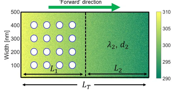
We use nanoporous Si as an example, and place the pores in various geometrical configurations to identify the parameters that determine rectification. The basis geometry we begin with is shown in Fig. 1. For computational efficiency we consider a two-dimensional (2D) simulation domain of length Lx = 1000 nm in the x-direction and width Ly
= 500 nm in the y-direction. The asymmetry is created by placing the pores only in one part (porous region) of the material. We investigate the influence of porosity, pore density (as a function of inter-pore distance, d) and pore position relative to the device left/right boundary. Porosity (φ) is given as the total area of the pores (number of pores × area of each pore) over the total simulation domain area (given by the width × total length i.e. LT in Fig.
We compute the thermal conductivity in the materials by solving the phonon Boltzmann transport equation using the Monte Carlo method as we described in our previous works [24-26]. The Monte Carlo (MC) approach offers great flexibility of geometrical configurations and parametric control over the scattering mechanisms that the phonons undergo, while still allowing very good accuracy [24, 26] and large micrometer size simulation domains. Further details on the Monte Carlo simulation approach we employ and the assumptions made therein can be found in the Appendix.
In the structures we consider, the domain is populated with circular pores of different arrangements. Each pore has a diameter of 50 nm. The choice of 50 nm is indirectly related to the phonon mean-free-path of pristine Si, λpp = 135 nm, mostly though, for computational
reasons: namely, for achieving diffusive transport we need channel dimensions of the order of several mean-free-paths, but not necessarily drastically larger to keep computational time manageable. Then, we need to deploy several pores into the domain, so we have used diameters smaller than the mean-free-path, but not so extremely small as to question the validity of the particle-based Monte Carlo method we employ. It seems that D = 50 nm is a size to satisfy these criteria, and that is the size we employed in several of our works over the years as well [41, 43, Chakraborty18, Chakraborty19JEM, Chakraborty19MT].
All phonons reflect on the pores, with the pore boundaries taken to scatter all incident phonons in a specular fashion [24]. While systems with asymmetric roughness do have a thermal rectification effect [27], in this work we leave the effect of roughness aside, and focus on the geometrical configurations of the pores. The basis simulation domain with 8% porosity is shown in Fig. 1. The coloring indicates the thermal gradient between the hot side with temperature TH = 310 K (yellow) and the cold side with TC = 290 K (green). The
green arrow on top of the schematic indicates the ‘Forward’ direction of heat flow, which we define when the pores are placed near the left, ‘hot’ contact, while keeping the ‘cold’ side empty of pores, thus creating an asymmetry in the transport direction. The thermal conductivity in this Forward direction is denoted as κF. Next, the structure is ‘flipped’ by
rotating it 180 degrees such that the pores are now on ‘cold’ side while keeping the ‘hot’ side empty of pores. The thermal conductivity in this ‘Reverse’ direction is denoted as κR.
F 1
R
R
(1)
We do not consider any modifications in the phononic bandstructure in the presence of pores, even if they are placed in periodic arrays. For the bandstructure to be modified, the requirement is that the wave-type carriers should remain coherent in distances several time larger than their wavelengths, as well as through several periods of the pore structure that forms the ’metamaterial’. Phonon-phonon scattering (with mean-free-path ~ 135 nm in Si) destroys coherence. The Monte Carlo approach we use is particle based and does not capture wave effects to begin with, however we are confident that ignoring bandstructure modifications is fully justified [28, 29].
III.
Results
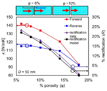
Rectangular nanoporous arrangements – influence of asymmetry: We begin our investigation by considering rectangular arrangements of pores as in Fig. 1 and the schematics in Fig. 2. Figure 2 summarizes the effect of asymmetry on the thermal rectification (R) in this type of geometrical configuration. To change the asymmetry, we begin with placing pores on the left of the domain/material, and then gradually add more and more layers separated by an inter-pore distance d, until the material becomes fully porous symmetric. We denote this asymmetry as the increasing average porosity (φ) of the material with the addition of porous layers. Examples of the typical geometries considered, with porosities of 6% and 10% for both ‘Forward’ and ‘Reverse’ configurations, are shown in the geometry panels above Fig. 2. In Fig. 2 we plot the thermal conductivity κ as a function of porosity φ on the left y-axis. The ‘Forward’ direction thermal conductivity (𝜅F)
is plotted by the red line, whereas ‘Reverse’ 𝜅R is by the blue line. The rectification R, is
given by the purple line and indicated on the right y-axis.
First, we observe that the largest difference between 𝜅F, and 𝜅R is observed for the
lower porosity case, where the pores are placed all the way to the edge of one side. For that case (φ = 6%) a difference of ~ 30 W/mK between κF and κR is observed. This gives the
conductivity decreases, but the difference in 𝜅F and κR also decreases, which reduces
rectification. At φ = 18% the pores are uniformly distributed throughout the simulation domain and no rectification is observed. Thus, structural asymmetry in the transport direction (x-direction) gives rise to thermal rectification as also observed in previous theoretical [16, 17, 20] and experimental works [30, 31]. In Fig. 2, we can clearly observe that the κF is larger compared to 𝜅R, which means that the hot phonons with shorter MFPs
encountering the pores suffer less. In the κR situation (when the structure is ‘flipped’), the
phonons that propagate from the pristine left (hot) to the porous right (cold), however, suffer more as by the time they reach the cold right side they develop longer MFPs.
This behaviour can be understood through a simple application of Matthiessen’s rule. Under this assumption, we consider the fact that R is actually determined by the change in transport properties of phonons as they encounter the pores while at high temperature regions (shorter MFPs), or while at lower temperature regions (longer MFPs). A simple model that can predict this behaviour is obtained by splitting the material system into two regions of length Li, that determine the total thermal resistance when added together as
ρT𝐿T = ρ1𝐿1+ ρ2𝐿2, where ρ𝑖 are the thermal resistivities of each region which are
weighted by the length of each region. Equivalently:
𝐿T
𝜅T
=
𝐿PRISTINE
𝜅PRISTINE
+
𝐿POROUS
𝜅POROUS
(2) The thermal conductivities in each region are proportional to the MFPs of phonons in each region as coupled together using Matthiessen’s rule as:
1 𝜅T
~
𝐿PRISTINE
𝜆PRISTINE
+
𝐿POROUS
𝜆POROUS
(3) where 𝜆PRISTINEis the temperature dependent Umklapp 3-phonon scattering MFP for Si
(𝜆PRISTINE=λpp = 135 nm at T = 300 K) and
𝜆
POROUS is the MFP in the porous region, which isgiven by the combination of two different scattering mechanisms, the Umklapp scattering MFP λpp and the pore scattering MFP, which we take as d, the average distance between
the pores. Thus, the MFP in the porous region is given by:
1 𝜆POROUS
=
1
𝜆pp
+
1Considering the thermal conductivity in the Forward direction (𝜅F), when pores are
placed closer to the hot junction as in Fig. 1, we then have:
𝜅F
~
(11 𝜆H+1 𝑑
)𝐿𝐿H T
+
𝜆C𝐿C
𝐿T (5)
where
𝜆
H < λpp < λC since the two regions are on the hotter/colder sides of the averagetemperature. Similarly, in the reverse direction we have:
𝜅R
~
𝜆H𝐿H𝐿T
+
(1
1 𝜆C+
1 𝑑
)𝐿C
𝐿T (6)
Inserting Eq. 5 and Eq. 6 in Eq. 1 we can estimate the rectification R.
The dashed-black line in Fig. 2 shows the rectification R calculated using Eq. 1 with
λH = 117 nm for the hot side (TH = 310 K) as and λC = 150 nm for the cold side (TC = 290
K), taken from Jeong et al. [32] and verified by our simulator. Note that the model only provides the rectification R, and not thermal conductivity values, as we only have proportionalities to the MFPs in Eq. 5 and Eq. 6. Using Eq. 1 and the lengths of the different porous regions, R values for all porosities are calculated, and a very surprising match to the Monte Carlo results is observed (black versus purple lines in Fig. 2) using the values of λH
andλC above.
Thus, based on this reasoning, what is important for rectification is the formation of the regions which force phonons from the hot side in the ‘Forward’ direction to interact as differently as possible with phonons reaching there from the cold side during the ‘Reverse’ direction. The closer the porous region is to the contacts, the larger the differences between the λH and λC, which in our simulations varies almost linearly between the two contacts [32,
and λC (if we consider at first order λH and λC as the mean-free-paths in the middle of the
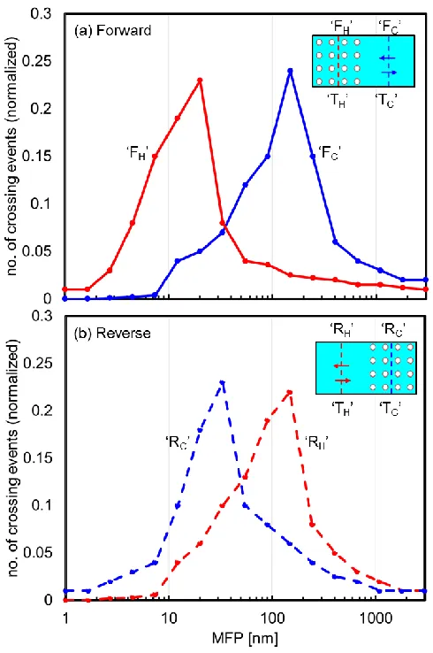
corresponding porous and the pristine regions, respectively), and rectification decreases. Influence of pores on mean-free-paths: In order to further clarify the role that the phonon mean-free-paths (MFPs) play in rectification we look at the spectral propagation of phonons through the network of the pores. The overall MFP of phonons is extracted in two places in the material in the middle of the porous region and in the pristine material region, as indicated by the vertical lines in the insets of Fig. 3. We then extract the MFP distributions for the case of the ‘Forward’ and the ‘Reverse’ structure cases. These are shown in Fig. 3a and 3b, respectively. To do this, for every phonon that crosses the dashed vertical lines we record the absolute time that the phonon last scattered before crossing the line, and the time that the phonon scatters after crossing the line. Using this interval time and the phonon velocity, we compute the phonon MFP. Thus, we have four MFP distributions, two for the ‘Forward’ structure (Fig. 3a) and two for the ‘Reverse’ structure (Fig. 3b). We label the different cases ‘FH’ (for forward-hot porous side – solid red line in Fig. 3a), ‘FC’ (for
forward-cold pristine side – solid blue line in Fig. 3a), ‘RH’ (for reverse-hot pristine side –
dashed red line in Fig. 3b), and ‘RC’ (for reverse-cold porous side – dashed blue line in Fig.
3b). These distributions are the combined effective scattering MFP of the phonons due to phonon-phonon scattering and pore boundary scattering.
In the pristine non-porous regions the MFP is equivalent to the pristine 𝜆pp of
phonons, but in the porous regions the overall MFP < 𝜆pp since pore boundary scattering is
also added. When the device is ‘flipped’ from the ‘Forward’ to the ‘Reverse’ case, the spectrum of the ‘hot’ side shifts from the solid red line to the dashed-red line and for the ‘cold’ side it shifts from the solid blue line to the dashed-blue line. The asymmetry in the shift of cold-to-hot and hot-to-cold with respect to MFPs points directly to the reason that rectification is created. From the data in Fig. 3a, in the ‘FH’ case (porous region) the MFP
is ~ 29 nm (compared to 33 nm from the analytical evaluation of Matthiessen’s rule with 𝜆H
= 117 nm and d = 50 nm). When the device is ‘flipped’ in Fig. 3b, the ‘RC’ case (porous
region) has MFP ~ 33 nm (compared to 37.5 nm from the analytical evaluation of Matthiessen’s rule with 𝜆C = 150 and d = 50 nm). Interestingly, the Monte Carlo computed
MFP changes by 17% when the device is ‘flipped’, (i.e MFPF/ MFPR - 1 = ~17%) very
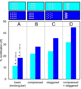
Rectangular nanoporous arrangements - influence of pore positions and density: To better understand the geometric details that influence rectification further, we perform a series of simulations by altering the position, inter-pore spacing, and porous’ regions effective resistance (the last is achieved by changing from an aligned to a staggered pore configuration) [26]. In Fig. 4 we show the rectification achieved by the porous geometries illustrated in the depicted schematics. The first series of simulations begin with the rectangular arrangement of pores located at the left side at a distance of 200 nm (~2 MFPs) from the left contact (𝑥 = 200 nm). The pores are located at distances d = 50 nm with respect to each other (light-blue, upper-left most schematic). We then investigate the effect of geometrical features on the rectifications as follows: i) by changing inter-pore distance, d, and making the structures more ‘compressed’, thus increasing thermal resistance; (still keeping the number of pores the same), ii) by staggering the overall geometry, thus reducing the line-of-side [34-36], also increasing the pore region resistance. iii) by combining effects (i) and (ii) i.e. reducing the inter-pore distance and staggering the pores.
First, we look at the rectification results shown by the light-blue bars (𝑥 = 200 nm) in Fig. 4. We start from the basis (rectangular) arrangement of pores (labelled arrangement ‘A’ on the figure) with a porosity of 8% and pore diameter D = 50 nm which provides 11% rectification. Reducing the inter-pore distance (arrangement ‘B’) increases rectification to 20%, then by staggering every alternate line of pores i.e. by moving the pores by 50 nm in the y-axis (arrangement ‘C’), an additional small rectification is added to reach 24%. The combination of the two further increases rectification to 31%(arrangement ‘D’) (Note that in this last case we reduced the inter pore distance even further to d = 12.5 nm). This indicates that the larger the resistance of the rectifying region/junction, the larger the rectification that can be achieved.
the phonons encountering the pores have MFPs λH = 120 nm (> λpp = 135 nm since T = 308
K), while in the ‘Reverse’ direction, they have MFP λC = 147 nm (since T = 292 K). On the
other hand, in the light-blue, 𝑥 = 200 nm case, the numbers are slightly closer together, i.e. λH = 124 nm (T = 306 K) in the ‘Forward’ direction and λC = 143 nm (T = 294 K) in the
reverse direction. (Note that here we have considered the temperature of the beginning of the pore region that is closer to the corresponding contact to report the MFPs). The larger the differences in the MFPs of the phonons when they encounter the pores in the ‘Forward and ‘Reverse’ directions, the larger the rectification, and that is why the systems which place the pores closer to the device edge have larger rectification. The simple reason is that the longer the phonon MFPs, the more phonons are affected by nanostructuring (within the Matthiessen’s rule picture), and the larger the difference between the MFPs of the phonons when they encounter the porous regions in the two configurations, the larger the rectification. As a simple first order verification, inserting the above values in the model of Eqs. 5-6, provides values for R ~ 18% for dark-blue, 𝑥 = 100 nm caseandR ~ 13% for the light-blue, 𝑥 = 200 nm case, very similar to the ones that result out of the simulation (R ~ 18% and R ~ 11%, respectively). It seems that the choice of picking the MFPs at the beginning of the porous regions closer to the contacts provides this very good match. Following the same geometrical arrangements, ‘A’ – ‘D’ in the dark-blue cases (like in the light-blue, cases) we observe an increased rectification for the x = 100 nm cases at all cases (compare the dark-blue bars to the light-blue bars). Bringing the pores closer together to d/2 = 25 nm in the x-direction (‘B’ in Fig. 4) increases rectification to 28%, introducing staggering (‘C’) provides another increment to 35%, and combining the two geometries (and enforcing an even smaller separation) as in the ‘D’ arrangement, the overall rectification jumps to as high as 44%.
In order to better understand the increase in rectification as we move pores closer to the device edge, we compare the contributions of κF and κR to rectification of the same
structures in Fig. 4. In Fig. 5 we show the corresponding κF and κR by the red and blue bars,
for the same structures "A" - "D" respectively. Figure 5 shows that, as expected, both κF
and κR drop as the structure becomes more resistive, but the reduction in κR (blue bars) is
larger for all cases, and this is the primary reason behind the rectification improvements. For instance, the κR observed in the light-blue, 𝑥 = 200 nm case drops by ~29% when
the corresponding κR drop in the dark-blue, 𝑥 = 100 nm case is ~36%. We can draw a couple
of conclusions from these observations: i) the larger drop in κR compared to that of κF is
what increases rectification in these structures, and ii) that κR reduces more as pores are
brought closer to the cold domain edge. That is again in agreement with the simple Matthiessen’s rule based consideration, which states that it is the long MFP colder phonons that are affected more when encountering the porous regions.
Thus, the greatest rectification is seen for the most asymmetric case, where the temperature-dependent MFPs of phonons differ as much as possible between the ‘Forward’ and ‘Reverse’ directions. Hence, as placing the pores closer to the edge enhances rectification, from here on we consider the 𝑥 = 100 nm basis case to examine further geometrical configurations.
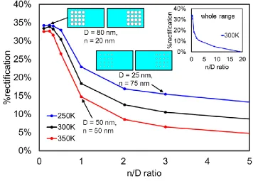
Influence of neck/diameter geometrical considerations and temperature: To further understand the interplay between the geometrical features and the mean-free-path (MFP) in determining rectification, we examine the combination of pore diameter (D) and the corresponding interpore distance (neck, n) in determining thermal resistance in these nanostructures (our geometries so far have n = 50 nm and D = 50 nm, which corresponds to to ratio n/D = 1). Different diameters and neck sizes will interact with different phonon MFPs differently. In Fig. 6 we show the rectification simulation results for structures with different pore sizes (and neck sizes) as well versus different n/D ratios, for 3 different temperatures. Some typical geometries are indicated in the insets. First we note that that reduced n/D ratio gives higher thermal resistance, which gives greater rectification until a ‘cut-off’ neck size.
The saturation in rectification for small n/D is explained as follows: Rectification is achieved when the overall mean-free-path (MFP) near the hot side of the ‘Forward’ direction structure, is different than the MFP near the cold side of the ‘reverse’ direction structure. When the scattering mean-free-path (determined by the neck distance and diameter) is of the order of the phonon mean-free-path, λpp, then variations in the geometry
will have an influence in the overall MFP. As the neck size is decreased to sizes much smaller than λpp, then boundary scattering dominates the overall MFP in either the ‘Reverse’
reducing neck size below this saturation point further, gives diminishing returns for rectification since it is already much smaller than λpp at that point.
In Fig. 6 we also show the effect of temperature. We have performed simulations for the same set of different geometries at two more temperatures, one higher (TH = 350 K), and
one lower (TH = 250 K) than the nominal room temperature. For a given geometry, higher
temperatures reduce the phonon λpp due to stronger phonon-phonon scattering (λpp = 100 nm
for TH = 350 K), and increase their influence in determining thermal resistance over the pore
scattering, which reduces rectification. In contrast, lower temperatures increase the phonon MFPs (λpp = 220 nm for TH = 250 K), which reduce their influence in determining thermal
resistance over the pore scattering (or the pore influence becomes bigger), which increases rectification.
A different material, other than Si, will have different phonon MFPs, and the geometry will then need to be adjusted accordingly, such that the dominant heat carrying phonons actually interact effectively with the underlying nanopore geometry. For example, in materials with short phonon MFPs (as also in the case of Si at high temperatures), the neck size needs to be smaller compared to materials with larger phonon MFPs in order to achieve the same level of rectification (similar to how Si with smaller phonon MFPs at elevated temperatures requires a smaller n/D ratio to achieve the same rectification compared to Si at lower temperatures with larger MFPs in Fig. 6). Thus, we believe our conclusions can be generally applied to other materials as well, in which case the underlying geometry dimensions need to be adjusted to the MFP of the specific material.
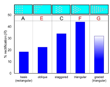
Influence of exposed surface area and grading: From the simple model presented
In the simulation results shown in Fig. 7 we begin again with the basis ‘A’ structure of 8% porosity. In order to examine the effect of increasing the interface area that separates the two regions, we rearrange the pores in an oblique configuration (‘E’) seen in the panel above Fig. 7. We find that increasing the interface area, i.e. increasing the surface area where rectification happens, increases R to ~ 22% overall (comparing the ‘A’ with ‘E’ case bars in Fig. 7). By following the same logic for staggered pores (‘C’) and exposing both sides we consider a triangular arrangement of pores (arrangement ‘F’) which gives an amplified R = 45% (as compared to R = 34% of the simple staggered arrangement ‘C’).
However, by extending this structure to get a graded geometry throughout the domain (graded-triangular) arrangement ‘G’ in Fig. 7), does not lead to any more rectification improvements. In fact, R drops to ~31% from 45% that is achieved by the triangular structure (case ‘F’), which is more asymmetric and divide the domain into two discrete porous and non-porous segments. In the fully graded ‘G’ case phonons interact with the pores throughout the domain. It could be argued that that a graded porous structure would provide a small degree of rectification locally, but that would extend to the entire channel, and the aggregated effect could be significant. Our simulations show, however, the reverse, namely that that discontinuous regions (junctions) provide a greater rectification than graded geometries in our Si structures, as also indicated in other materials [12, 13, 17, 20, 37-40], as the differences between the phonon MFPs in the ‘Reverse’ and ‘Forward’ directions in each segment of the structure are now smaller.
In the second structure column (‘H’) in Fig. 8, by introducing smaller nanopores of diameter D = 10 nm to the existing base structures in a hierarchical fashion we increase the effective pore density. This gives R = 51% for the triangular case compared to 24% in the rectangular case (green versus blue bars for structures ‘H’ of Fig. 8). We then reduce the inter-pore distance from d = 50 nm to d/2 = 25 nm in the x-direction (column ‘C’ in Fig. 8), thus making the structures more ‘compressed’ with increased thermal resistance. Structure ‘C’ in the triangular arrangement causes an increase to R = 57%, compared to 28% in the rectangular ‘C’ case.
Finally, by combining the effects of density and hierarchical nanopores we get a maximum rectification of R = 61% in the combined hierarchical structure (arrangement ‘I’) for the triangular case in Fig. 8. Compared to the arrangement ‘D’, the compressed rectangular case given by the white bar with blue-dashed outline in Fig. 8, the triangular configuration provides a 35% increase in heat rectification. This further stresses the importance of the larger rectifying junction length/area, as well as the high thermal resistance of the porous region, rather than the graded porous configurations in the structures we have investigated.
IV. Conclusions
V. Acknowledgements
VI. Appendix: Single Phonon Monte Carlo Method
This section gives details about the Monte Carlo approach we employ, its validation, and the assumptions related the scattering term used. Full details can be found in our previous works [24, 41] . The simulation process is as follows: The simulation domain of size Lx = 1000 nm × Ly = 500 nm is initialized with a ‘Hot’ and ‘Cold’ end, set at TH = 310
K and TC = 290 Krespectively.
Phonons are then allowed to enter the simulation domain from either side and alternate between free flight and scattering. The time a phonon spends in the simulation domain is recorded as its ‘Time-Of-Flight’ (TOF). Phonons are initialized based on energy, frequency, polarization, and velocity. We use the dispersion relation ω(q) and corresponding group velocities vg(q) as described by Pop et al. [42] in Eq. A1 and Eq. A2 below:
ω
q vsq cq2 (A1)d
d
g
q
v
(A2)where q is the wave vector norm and vs and c are fitting parameters to match the thermal
conductivity of bulk Si in the [100] direction. The dispersion coefficients we use are vs =
9.01 × 10³ ms-1 and c = -2 × 10⁻⁷ m2s-1 for the longitudinal acoustic (LA) branch, and vs =
5.23 × 10³ ms-1 and c = -2.26 × 10⁻⁷ m2s-1 for the transverse acoustic (TA) branches [43]. Following common practice, the contribution of optical phonons is neglected as they have low group velocities and do not contribute significantly to phonon transport [44-47].
Phonons in the simulation domain either scatter, or are in free flight. During free flight, the position r at time t of the phonon is given by the equation:
ti ti1 g tr r v (A3)
1/ 2
1 TA 2
TA, U U
1/ 2 B 0 sinh for B for k T (A4)
where
is the frequency, T the temperature,B
UTA = 5.5 × 10⁻¹⁸ s, and
1/2 is the frequencycorresponding to q = qmax/2. These equations and parameters are well-established and often
used to describe relaxation time in phonon Monte Carlo simulations for Si [42-45, 48]. Three phonon scattering causes a change in the energy, and thus the temperature (T) of the simulation domain ‘cell’ where scattering took place (we use a 0.1 nm domain discretization). Every time this happens the ‘cell’ temperature either rises or falls. The link between energy and temperature is given by:
V ( , ) W exp 1 k i i i
p i i
i
E g D p
T
(A5)where 𝜔 is the frequency, 𝑇 the temperature, D the density of states at given frequency and branch polarization, and 𝑔𝑝 the polarization branch degeneracy, and V is the volume of the ‘cell’. The dissipation/absorption of energy from each ‘cell’ in this way establishes a temperature gradient under a continuous flow of phonons (shown in Fig. 1 with the yellow to green color scheme). A scaling factor (W = 4×10⁵) is also introduced to scale the number
of phonons simulated to the real population of phonons from 6×1010 μm-3 that are present at 300 K for computational efficiency [41].
The total energy entering and leaving the simulation domain is calculated by the net sum of the corresponding phonon energies that enter/exit at the hot and cold junctions as calculated by Eq. A5. We label the total incident energy from the hot junction as
E
inH and the
H H C C
in out in out
E E E E
n TOF (A6)
where n is the total number of phonons simulated (typically 1 million) and TOF is the average time-of-flight of all phonons. The thermal conductivity (κ), is then calculated using Fourier’s law.
s T (A7)
Next, to account for the fact that the length of the simulated domain (Lx) is smaller
than some phonon wavelengths, especially at lower temperatures, a scaling of the simulated thermal conductivity (κs) is needed to compute the final thermal conductivity κ as[32]:
X pp sX
L
L (A8)
where λpp is the average phonon mean-free-path (MFP) of Si. In previous work simulations
References:
[1] M. Verdier, Y. Han, D. Lacroix, P.O. Chapuis, and K. Termentzidis, J. Phys. Mater. 2, 15002 (2019).
[2] M. Verdier, D. Lacroix, and K. Termentzidis, Phys. Rev. B 94, 1 (2018). [3] C. J. Foss and Z. Aksamija, 2D Mater. 6, 025019, (2019).
[4] J. Cao, J. D. Querales-Flores, A. R. Murphy, S. Fahy, and I. Savić, Phys. Rev. B 98, 1 (2018).
[5] I. Zardo, R. Rurali, Green Sustain. Chem. 17. Pp. 1-7 (2019).
[6] B. Lorenzi, R. Dettori, M. T. Dunham, C. Melis, R. Tonini, L. Colombo, A. Sood, K. E. Goodson, and D. Narducci, J. Electron. Mater. 47, 5148,
(2018).
[7] M. Ohnishi and J. Shiomi, APL Mater. 7, (2019).
[8] A. Malhotra, K. Kothari, and M. Maldovan, J. Appl. Phys. 125, (2019). [9] C. Starr, J. Appl. Phys. 7, 15 (1936).
[10] Sergei Gluchko , Roman Anufriev , Ryoto Yanagisawa , Sebastian Volz , and Masahiro Nomura, Appl. Phys. Lett. 114, 023102 (2019).
[11] J. J. Martinez-Flores, Dinesh Varshney, and J. Alvarez-Quintana, Appl. Phys. Lett. 113, 264102 (2018).
[12] X. Yang, D. Yu, B. Cao, and A. C. To, ACS Appl. Mater. Interfaces 9, 24078 (2017).
[13] D. Sawaki, W. Kobayashi, Y. Moritomo, and I. Terasaki, Appl. Phys. Lett. 98, 081915 (2011).
[14] Y.Wang, S.Chen, and X. Ruan, Appl. Phys. Lett. 100, 163101 (2012). [15] Yue-Yang Liu, Wu-Xing Zhou, Li-Ming Tang, and Ke-Qiu Chen, Appl.
Phys. Lett. 105, 203111 (2014)
[16] M. Criado-Sancho, F. X. Alvarez, and D. Jou, J. Appl. Phys. 114, (2013). [17] C. L. Chiu, C. H. Wu, B. W. Huang, C. Y. Chien, and C. W. Chang, AIP
[18] M. Terraneo, M. Peyrard, G. Casati, Phys. Rev. Lett. 88, 9, 4302 (2002). [19] R. Dettori, C. Melis, R. Rurali, and L. Colombo, J. Appl. Phys. 119, (2016). [20] Z. Yu, L. Ferrer-Argemi, and J. Lee, J. Appl. Phys. 122, (2017).
[21] H. Machrafi, G. Lebon, and D. Jou, Int. J. Heat Mass Transf. 97, 603 (2016).
[22] Nuo Yang, Gang Zhang, and Baowen Li, Appl. Phys. Lett. 95, 033107 (2009).
[23] A. Yousefzadi Nobakht, Y. A. Gandomi, J. Wang, M. H. Bowman, D. C. Marable, B. E. Garrison, D. Kim, and S. Shin, Carbon, Elsevier, N. Y. (2018).
[24] D. Chakraborty, S. Foster, and N. Neophytou, Phys. Rev. B 98, 115435 (2018).
[25] D. Chakraborty and L. de S. Oliveira, J. Electron. Mater. 48, 1909 (2019). [26] D. Chakraborty, S. Foster, and N. Neophytou, Mater. Today Proc. 8, 652
(2019).
[27] N. A. Roberts and D. G. Walker, Int. J. Therm. Sci. 50, 648 (2011). [28] M.S. Jeng, R. Yang, D. Song, and G. Chen, J. Heat Transfer 130, 42410
(2008).
[29] Y.C. Hua and B.Y. Cao, J. Comput. Phys. 342, 253-266 (2017).
[30] M. Schmotz, J. Maier, E. Scheer and P. Leiderer, New J. Phys. 13 113027 (2011).
[31] H. Tian, D. Xie, Y. Yang, T.-L. Ren, G. Zhang, Y.-F. Wang, C.-J. Zhou, P.-G. Peng, L.-G. Wang, and L.-T. Liu, Sci. Rep. 2, 523 (2012).
[32] C. Jeong, S. Datta, and M. Lundstrom, J. Appl. Phys. 111, (2012). [33] M. Maldovan, J. Appl. Phys. 110, 114310, (2011).
[34] G. Romano and J. C, Grossman. Phys. Rev. B. 96, 115425 (2017).
[36] W. Park, G. Romano, E. C. Ahn, T. Kodama, J. Park, M. T. Barako, J. Sohn, S. J. Kim, J. Cho, A. M. Marconnet, M. Asheghi, A. M. Kolpak, and K. E. Goodson, Sci. Rep. 7, 1 (2017).
[37] S. Basu and M. Francoeur, Appl. Phys. Lett. 98, 1 (2011).
[38] Wei-Rong Zhong, Wei-Hao Huang, Xi-Rong Deng, and Bao-Quan Ai, Appl. Phys. Lett. 99, 193104 (2011).
[39] Xue-Kun Chen, Jun Liu, Zhong-Xiang Xie, Yong Zhang, Yuan-Xiang Deng, and Ke-Qiu Chen, Appl. Phys. Lett. 113, 121906 (2018).
[40] W. Kobayashi, Y. Teraoka, and I. Terasaki, Appl. Phys. Lett. 95, 171905, (2011).
[41] S. Wolf, N. Neophytou & H. Kosina. Journal of Applied Physics, 115(20), 204306, (2014).
[42] E. Pop, R. W. Dutton, & K. E. Goodson. Journal of Applied Physics, 96(9), 4998-5005, (2004).
[43] S. Wolf, N. Neophytou, Z. Stanojevic, & H. Kosina.. Journal of electronic Materials, 43(10), 3870-3875, (2014).
[44] S. Mazumdar, and A. Majumdar. Monte Carlo Study of Phonon Transport in Solid Thin Films including Dispersion and Polarization. ASME J. Heat Transfer, 123, pp. 749–759, 2001.
[45] D. Lacroix, K. Joulain, & D. Lemonnier. Physical Review B, 72(6), 064305, (2005).
[46] Q. Hao, G. Chen, and M.S. Jeng, J. Appl. Phys. 106, 114321, (2009). [47] A. Mittal and S. Mazumder, Journal of Heat Transfer 132, 052402 (2010). [48] E. Pop, S. Sinha, & K. E. Goodson. Proceedings of the IEEE, 94(8),
1587-1601, (2006).
[49] J.P. M. Peraud, C. D. Landon, and N. G. Hadjiconstantinou, Annu. Rev. Heat Transf. 205 (2014).
Figure 1:
Figure 1 caption:
Schematic of the basis geometry simulated with porous region of length 𝐿1 and pristine region of length 𝐿2. Individual properties are assigned for each region, including average
phonon mean-free-path, (MFP) 𝜆 and average distance between pores (inter-pore distance)
𝑑. The total length of simulation domain is 𝐿𝑇. In all Monte Carlo simulations we set 𝐿𝑇 = 1000 nm. The coloring indicates the established thermal gradients when the left and right contacts are set to TH = 310 K (yellow) and TC = 290 K (green), respectively. The green
Figure 2:
Figure 2 caption:
Monte Carlo simulations showing the effect of porosity (φ) in the rectangular, ordered pores configuration on thermal conductivity, 𝜅 (left axis), and rectification, R (right axis). For each value of φ, the 𝜅 in the ‘Forward’ direction (𝜅F) is given by the red line, while the𝜅 in the
Figure 3:
Figure 3 caption:
[image:25.612.181.426.103.472.2]Figure 4:
Figure 4 caption:
Figure 5:
Figure 5 caption:
Figure 6:
Figure 6 caption:
The rectification dependence (y-axis) on the pore and neck sizes – given by the neck/diameter (n/D) ratio (x-axis), and the mean temperature of the simulation domain. Three temperature ranges are examined Tavg = 350 K (light-blue line) for TH = 360 K to TC
= 340 K, Tavg = 300 K (blue line) with TH = 310 K to TC = 290 K and Tavg = 250 K (purple
line) with TH = 260 K to TC = 240 K. The rectification for whole range of n/D values
simulated for the Tavg = 300 K (blue line) case is given as an inset on the top right corner.
Figure 7:
Figure 7 caption:
The dependence of thermal rectification on the exposed junction surface area and pore grading. Five cases are examined, and the geometries simulated are given above the bar chart. These are: i) the basis (rectangular) arrangement of pores (‘A’) with pore diameter D
Figure 8:
Figure 8 caption:
The rectification dependence on the construction of the triangular regions, and the hierarchical incorporation of smaller nanopores (D = 10 nm) in between the bigger ones (D
= 50 nm). Four cases are examined, each for both rectangular geometries (dark-blue bars) and triangular geometries (green bars). The geometries simulated are shown in the panel above the figure. These are: i) the basis arrangement of pores (‘A’) for both rectangular and triangular configurations given by dark-blue bars or green bars, respectively. For all pores