FPGA Based Intelligent Co-operative Processor
in Memory Architecture
Zaki Ahmad, Reza Sotudeh, D. M. Akbar Hussain, Shahab-ud-din
∗Abstract—In a continuing effort to improve com-puter system performance, Processor-In-Memory (PIM) architecture has emerged as an alternative so-lution. PIM architecture incorporates computational units and control logic directly on the memory to pro-vide immediate access to the data. To exploit the potential benefits of PIM, a concept of Co-operative Intelligent Memory (CIM) was developed by the in-telligent system group of University of Hertford-shire, based on the previously developed Co-operative Pseudo Intelligent Memory (CPIM). This paper pro-vides an overview on previous works (CPIM, CIM) and realization of CPIM over two scenarios, cumu-lative successive addition, and non-cumucumu-lative suc-cessive addition, using Nexar 2004 EDS tool as a design environment to target device (SPARTAN II, XC2S300E-6PQ208C).The performance (speedup) is then measured against an SISD without signifi-cant performance acceleration methods to ensure a speedup assessment obtained against base-line archi-tecture.
Keywords: Co-operative Intelligent Memory (CIM), Processor-in-Memory (PIM), Shared memory, CP U−major, CP U−minor, Observer, Task optimizer
1
Introduction
Due to the growing processor-memory performance gap, those applications having high degree of locality are able to exploit the full performance capability of the current microprocessors. Applications that suffer frequent cache or TLB misses find their performance limited by the speed of the memory system. A concept, Processor-in-Memory (PIM) architecture, IRAM, has been proposed to improve system performance by the computer archi-tecture group of the University of Berkeley [1]. PIM ar-chitecture incorporates computational units and control logic directly on the memory to provide immediate access to the data. For class of tasks which are heavily reliant on
∗Manuscript submitted January, 2011 Dr. Zaki Ahmed is
working as a Principal Engineer at PILO (Pakistan Institute of Laser and Optics). Email: [email protected]. Prof. Reza So-tudeh works at the School of Electronics, Communication and Electrical Engineering, University of Hertfordshire, UK Email: [email protected]. Dr. M. Akbar Hussain is member of IEEE, IDA, IAENG and works at the Department of Electronic Systems Aalborg University, Niels Bohrs Vej 8, 6700 Esbjerg, Denmark. Email: [email protected]
memory to-memory iterative process [2][3][4][5][6][7][8], an extension of IRAM, Co-operative Intelligent Memory (CIM) was developed by the intelligent system group of University of Hertfordshire, based on previously devel-oped Co-operative Pseudo Intelligent Memory (CPIM), to reduce the performance gap between the processor and memory by partitioning computation through dividing workload between major (non-iterative) and minor (iter-ative) CPUs.
The choice of FPGA for the implementation of the pro-posed architecture was driven by the growth in the size and capabilities of programmable logic. Generally, there are two primary methods in conventional computing for the execution of algorithms. The first is to use hard-wired technology, either an Application Specific Integrated Cir-cuit (ASIC) or a group of individual components forming a board-level solution, to perform the operations in hard-ware. ASICs are designed specifically to perform a given computation, and thus they are very fast and efficient when executing the exact computation for which they were designed. However, the circuit cannot be altered af-ter fabrication. This forces a re-design and re-fabrication of the chip if any part of its circuits requires modification. This is an expensive process, especially when one consid-ers the difficulties in replacing ASICs in a large number of deployed systems. Board-level circuits are also somewhat inflexible, frequently requiring a board design and re-placement in the event of changes to the application.
Reconfigurable devices in the form of Field-Programmable Gate Arrays (FPGAs) contain an array of computational elements whose functionality is determined through multiple programmable configura-tion bits. These elements, known as logic blocks, are connected using a set of routing resources that are also programmable. In this way, custom digital circuits can be mapped to the reconfigurable hardware by computing the logic functions of the circuits within the logic blocks, and using the configurable routing to connect the blocks together to form the necessary circuits. However to do this the designer need a design environment that solves the system integration issues, where they can capture the hardware design, test and debug the system on the target FPGA. This paper describes some key characteristics of CPIM and CIM architecture and design flow to establish the basic methodology used in the implementation of proposed CPIM. The performance (speedup) over two scenarios, cumulative successive addition, and non-cumulative successive addition is then measured against an SISD without significant performance acceleration methods (by modern standards) to ensure a speedup assessment is obtained against base-line architecture. For this, we chose 68000 as a base-line. This choice was primarily driven by the rich instruction portfolio that covers all relevant addressing modes and the clear mapping of instruction and machine cycle to the 68000 hardware building block.
2
Architectures Description
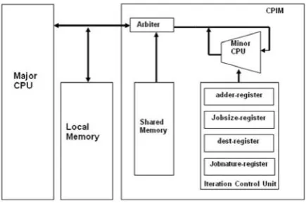
The CPIM and CIM architectures are shown in figure 1 and 2 respectively. The main CPU,CP U−major, has a conventional architecture and poses no real design con-straints on the CPIM architecture and backed up by a deep cache hierarchy and suffers high latency to access memory. The enhancement called CPIM, introducing a new block of memory (shared memory), shared through arbitration between CP U−major and task specific pro-cessor, CP U−minor, that consists of a small computa-tional unit performing iterative processing and an Iter-ation Control Unit (ICU). ICU provides an instruction format for the CP U−minor, consists of a set of regis-ters, namely address register (addr-register), job size reg-ister (job-size-regreg-ister), job nature regreg-ister (job-nature-register) and destination register (dest-(job-nature-register).
[image:2.595.310.528.49.196.2]A detailed discussion of the CPIM architecture with dis-tribution of workload and code optimization technique can be found in [9][10]. The CIM architecture (figure 2) differs from CPIM in terms of approach; instead of Von-Neumann (instruction and data are stored in a single memory) it requires a Harvard approach towards mem-ory (Separate memmem-ory for instruction and data). This approach may simplify read / write mechanism, partic-ularly as programs are normally read during execution, while data might be read or altered. Also establish a
Figure 1: CPIM Architecture
path for the extraction of vector components by mon-itoring the activity operating on the address and data buses. The detection of iterative tasks, conducted by an additional hardware unit called ”observer” having addi-tional knowledge of the location of specific logic blocks (CPIM) with reference to their operational capability.
Figure 2: CIM Architecture
The following jobs are performed by the observer;
• Extraction of vectors that characterize the iteration.
• Transfer of vector components with the related set of data into specific logic block.
• Removal of selected / corresponding iterative loop from the main stream.
A detailed discussion of the CIM architecture with design methodology, acceleration and speedup parameter can be found in [9][10]. Our CPIM and CIM architectures have the following characteristics:
[image:2.595.300.545.334.461.2]• Eliminates the overhead associated with the time it takes to fetch and execute the instruction in a specific program loop.
• No need for special instructions as required in the case of coprocessor.
• CP U−major (main CPU) can continue with other
operations while the CPIM is completing its allo-cated task.
The major characteristics that make CIM distinctive from the existing PIM systems, is its learning capability to gather intelligence from the current program execution profile.
3
Realization of CPIM
Along with the growth in the size and the functionality of application specific ICs, there has been a corresponding growth in the size and capabilities of programmable logic. This has made it possible to implement CPIM on FPGA. However to do this the designer need a design environ-ment that solves the system integration issues, where they can capture the hardware design, test and debug the sys-tem on the target FPGA. This section shows the use of a window based EDS tool (Nexar 2004, a window based electronics design software introduced by Altium limited) for FPGA design.
3.1
FPGA Design Flow
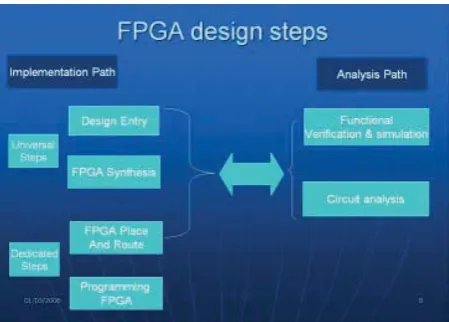
Design flow is the step by step methodology to go through the process of FPGA design. The design flow is shown in figure 3 and it can be seen that it is divided into five (5) basic steps:
• Design Entry or Capture H/W design: The first step of FPGA design flow describes the design that has to be implemented on FPGA.
• Functional Verification and Simulation: This step checks the logical correctness of design.
• FPGA Synthesis: This step converts design entry into logic blocks.
• FPGA Place and Route: Optimized the circuit and minimizes the length of interconnection.
• Circuit AnalysisThis step performs timing analy-sis.
• Programming to FPGA: Download FPGA pro-gramming file into target FPGA.
3.2
Design Environment
Nexar design environment ?? allows designing a digital system in an FPGA project as a set of Schematic sheets, VHDL codes, or using a mixture of Schematic and VHDL. For the designers, the choice of whether to use Schematic or VHDL based design entry comes down to their concept towards design. Those who think in software terms HDL are the better choice, and those are hardware oriented, schematic or the mixture of schematic and VHDL are the best choice. Schematic design is facilitated in Nexar by the inclusion of extensive libraries of synthesized, pre-verified IP components, including a range of processor cores, which can be simply dropped onto the schematic and connected together to form the system hardware. This is analogous to the way designers work at the board level with the physical ”off-the-shelf” components.
The concept of multi-board is very common at the system level design. Nexar provides a multi-sheet design method-ology, similar to the multi board design. Designers turn to multi-sheet design for various reasons, the primary one being project size; some projects are simply too large or complicated to fit on a single sheet. But even small design can benefit from a multi sheet approach. For example, the design may include various modular elements, and dividing those modules into individual documents would allow several designers to work on a project in parallel.
At the system level, Nexar provides a schematic-based design methodology to define system connectivity. The reason being that graphical schematic-based capture or design entry is more efficient for connecting functional blocks than HDLs, and allows complex systems to be cre-ated quickly at the component level. Along with IP-based components, Nexar includes a library of IP-based virtual instruments (as pre-synthesized models), such as logic an-alyzers, frequency counters/generators and I/O monitors that can be incorporated into the design at the schematic level to facilitate system testing and debugging. These in-struments have on-screen front panels analogous to their physical counterparts to provide a natural way for the designers to examine the working of their circuits, and to see inside the FPGA during the design process. Af-ter design entry, the compilation stage can verify that the design entry or captured source is free of electrical, drafting, and coding errors. Resolve any error found and re-compile the project to check.
3.3
Constraints On All Sides
con-straints to optimize the net-list. However, it is equally important to not over constrain the design, which will generally result in less than optimal results from the next step in the implementation process-physical device place-ment and interconnecting routing. Synthesis constraints soon become place and route constraints. Nexar provides a handy way to add the constraints file into the FPGA project by using Configuration Manager.
Integral to Nexar is a versatile FPGA-based develop-ment board called a Nano-Board that provides a re-configurable platform for implementing the design. The Nano-Board uses JTAG-based communication to both download the design to the on-board FPGA, and to in-teract with processor cores and instruments in the design once it has been downloaded to the target device (FPGA) housed on the removable daughterboard.
Synthesis stage can be run with the ”Devices” view con-figured in either ’Live’ or ’not Live’ mode. During syn-thesis, the source documents are translated into interme-diate VHDL files which are then synthesized into EDIF netlist, suitable for vendor Place and Route tools. Errors detected during synthesis are based on errors in the in-termediate files, so go back to the source files to fix any problems. After netlist synthesize, the design is auto-matically converted into the format supported internally by the FPGA vendors Place-and-Route tools. This stage ”Build” can be run with the Device view configured in ”live” or ”not live” mode. Running the tools at this stage can verify a design fit inside the chosen physical device. The end result of this stage is the generation of an FPGA programming file that will ultimately be used to program-ming the physical device with the design.
3.4
Program FPGA
Finally, the programming file, once successfully down-loaded to the device via the JTAG link, the text un-derneath the target device will change from ”Power” to ”Loaded” and any Nexus-enabled devices on the soft de-vices chain will be display as running.
3.5
Hardware Design
The major component of CPIM architecture described in figure 1, includes an optimized CPU, shared memory, an iteration control unit and an arbiter. Optimized CPU (CP U−minor) is a task specific processor that consists of a dedicated computation unit. The CPIM under dis-cussion equipped with a task ”cumulative Successive ad-dition” (An array of numbers is added and the result is stored in the defined memory location).
Shared memory is a SRAM-type memory, holding data related to the iterative job, having enough capacity to hold large frame synonyms with high resolution image frames. Iteration control unit provides an instruction for-mat for the CP U−minor. It consists of three registers,
namely Address register, Job size register and Job nature register. Address register is 24-bit wide, representing the starting address of the operand block. Once initialized, a counter will then increment a pointer, pointing to the next operand required by the task. Job-size register is 16-bit wide, representing the total number of operands (number of iteration involved in the iterative loop). Job-nature register is 8-bit wide, representing the Job-nature of Job. Destination register, two registers are required to hold the start and end address of the destination block.
[image:4.595.307.532.286.447.2]Arbiter facilitates the transfer of information between components. The processors in shared-memory multi-processor system request access to common resources through the system bus. When two or more processors share the same memory, some hardware mechanism is re-quired to make sure that only one processor can access the memory at a time. This can be achieved by using an arbiter in a shared memory system.
Figure 3: FPGA Design Steps
4
Conclusion
Figure 4: Cumulative Successive Addition
Figure 5: Non-Cumulative Successive Addition
References
[1] D. Patterson, T. Anderson, N. Cardwell, R. Fromm, K. Keeton, C. Kozyrakis, R. Thomas and K. Yelick. A Case for Intelligent RAM: IRAM. IEEE Micro, April 1997.
[2] Y. Kang, J. Torrellas and T. S. Huang, An IRAM Architecture for Image Analysis and Pattern Recog-nition. 14th International Conference on Pattern Recognition, 1998.
[3] M. Oskin et al., ”Active Pages: A computation model for intelligent memory”, IEEE, 1999.
[4] Y. Kang et al., ”FlexRAM: Towards an intelligent memory system”, ICCD, Oct 1999.
[5] J. Darper et al., ”The architecture of DIVA process-ing in memory chips”, ICS, June 2002.
[6] A. Saulsbury et al., ”Missing the memory wall: The case for processor/memory integration”, ICSA,May 1996.
[7] D. Burger et al., ”Memory bandwidth limitations of future microprocessors”,I SCA, Aug 1996.
[8] K. Mai et al., ”Smart memories: A modular recon-figurable architecture”, ISCA, June 2000.
[9] Zaki Ahmad ”Co-operative Intelligent Memory”, PHD thesis, University of Hertfordshire, United Kingdom, 2007.
[10] R. Sotudeh, Z. Ahmad, F. Bensaali ”Intelligent Co-operative Processor in Memory Architectures” The Mediterranean Journal of Electronics and Commu-nication, Vol. 3, 2007, pp 17-30.
[11] R. Boyle and R. Thomas ”Computer vision: A first course”, Blackwell Scientific Publications, 1988.
[12] R. Dougherty and A. Laplante, ”Introduction to REAL-Time IMAGING”, SPIE optical Engineering Press, 1995.
[image:5.595.42.280.262.471.2]