Ultrafast observation of electron hybridization and in-gap surface states
formation in Kondo insulator SmB6
Sanjay Adhikari1, Yanjun Ma2, Zach Fisk3, Jing Xia3, Chang-Beom Eom2, Cheng Cen1* 1Department of Physics and Astronomy, West Virginia University, Morgantown, West Virginia
26506, USA
2Department of Material Science and Engineering, University of Wisconsin-Madison, Madison,
Wisconsin 53706, USA
3Department of Physics and Astronomy, University of California, Irvine, California 92697-4575,
USA
*Correspondence to [email protected]
Abstract
Ultrafast electron dynamics capture important characters of many correlation phenomena. We report femtosecond optical pump-probe experiments in Kondo insulator SmB6. Transient profiles of electron relaxation, 4f heavy fermion plasma, and the strain wave are studied. The results indicate the onset of the f-d hybridization at 120 K, constant band gap within 20 K–100 K, and the formation of surface states below 20 K. Measurements are consistent in both single crystal and polycrystalline thin film, pointing to the observed phenomena’s robustness against defects and grain boundary scattering.
Introduction
Electron correlations usually give rise to exotic quantum phases with unusual properties. A current focus of condensed matter physics is to understand what electron correlation will bring to topologically ordered [1-4] materials including quantum Hall systems [5], quantum spin Hall systems [6] and topological insulators [7,8]. Kondo insulators (KI), in particular SmB6, are prototypical strongly correlated materials featuring f-electron physics and some quite unusual electronic properties. The recent theories of topological Kondo insulator (TKI) [9,10] have predicted in some KI materials, in particular SmB6, the existence of a topological nontrivial surface state with odd number of Dirac surface bands. In a nutshell, the strong interaction within the localized periodic dense array of f-magnetic-moments (so-called Kondo lattice) leads to reconstructions of the electronic structure and opens up [11] an energy gap at low temperatures due to the hybridization between conduction electrons and the highly renormalized f-electrons. When the Fermi level lies within such a Kondo energy gap, a KI is formed. The hybridization and odd parity wavefunction lead to strong spin-orbit coupling and give rise to a topological surface state [10] that dominates electron conduction at low temperatures. In particular, SmB6 is predicted to be a strong TI [10]. First principle calculations [12,13] have proposed a surface state with three Dirac bands at Γ and X/Y points in the (100) surface.
In the past two years tremendous experimental progress has been made on SmB6. Well-designed transport experiments revealed a low temperature resistance plateau associated with the surface layer [14,15]. Point-contact spectroscopy [16], Scanning tunneling microscope (STM) [17,18], angle resolved photoemission spectroscopy (ARPES) [14-16,19] and magnetometry [20] provided further evidences of the surface state at low temperature. Signatures of Dirac-like dispersion and topological nature of the surface state have also been discovered [20-24]. From all these recent work, a coherent picture of the SmB6 surface state with explicit correlation physics from underlying Kondo lattice is starting to emerge.
Relaxation dynamics of nonequilibrium systems have revealed many important problems in strongly correlated materials such as high Tc superconductors [25-28] and heavy fermion metals/semiconductors [29-31]. In this study, excited electron dynamics in SmB6 are investigated by optical pump-probe technique. Through the impulsive excitation of plasma oscillations, we are able to monitor the f electron hybridization directly. Photoexcited electrons-hole pairs recombine through interaction with thermal electrons and the lattice. Probing this process in time domain allows us to quantify the hybridization gap energy and sensitively detect the likely emergence of surface states at low temperature. To evaluate the robustness of the observed properties, experiments are performed on two type of samples of distinct crystalline characters: single crystal and polycrystalline (as grown) thin film.
Experimental Setup
SmB6 single crystals were grown using the aluminum flux method similar to previous works [15,23,24]. Thin films of SmB6 are deposited on top of MgO substrate by pulsed laser deposition (PLD). Details of material preparation can be found in the supplemental material [32]. Transport characterizations of the samples show similar temperature dependences of the resistance as previous reports (Fig. S1) [15,23]. Resistances in both single crystal and thin film samples saturate
below 4 K, indicating an insulating bulk and the possible formation of surface states at low temperatures.
Our pump probe setup consists of a homemade Ti:Sapphire oscillator producing 35 fs pulses centered at 840 nm (1.48 eV) with an 74 MHz repetition rate. The output of this oscillator pumps a Barium Beta Borate (BBO) crystal and generates a second harmonic beam centered at 420 nm (2.96eV). Both beams, with the 420 nm pulse acting as the pump and the 840 nm pulse as the probe, are focused to the sample surface with an aspheric lens. The pump and probe pulses are delayed with respect to one another using a translation stage. Pump intensity is modulated at 84 KHz by a photoelastic modulator (PEM). By lock-in detecting the sample-reflected probe intensity (R) at the same frequency, pump induced (PI) reflectivity change (∆R/R) is acquired. A balanced detection scheme is used to further suppress the background noise. Sample temperature is varied between 5 K and 294 K in a close cycle cryostat. To avoid laser heating at low temperatures, fluences as low as 0.1 μJ/cm2 are used in the measurements.
Data and Discussion
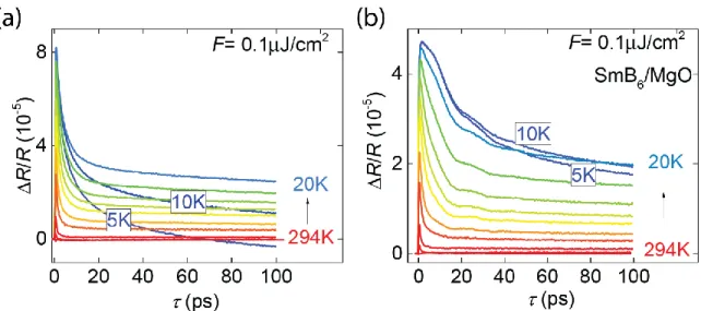
Time-resolved change in probe reflectivity measured at different temperatures are displayed in Figure 1. At zero delay, ∆R/R rises sharply due to the hot electrons generated by the pump pulse. Following the initial excitation, electrons quickly thermalize through electron-electron scattering and phonon emissions. During this process, energies of hot electrons experience significant relaxation and the photocarrier density is greatly amplified, which is represented by the sub-picosecond rise of the pump-probe signal close to zero delay. After reaching the maximum amplitude, ∆R/R then gradually recovers toward the level prior to the pump excitation. During the recovery, both monotonic decays and coherent oscillations are observed, which will be discussed separately in the following text.
First, we analyze the monotonic decay using a phenomenological Rathwarf-Taylor (RT) model [33]. This model, originally developed for quasiparticle relaxation in superconductors [34,35], has also been proven useful in describing the ultrafast carrier dynamics in heavy fermion metals and semiconductors [29,36]. As pointed out by Rathwarf and Taylor, phonons play important roles in assisting electron relaxation in narrow bandgap systems. In these systems, interband non-radiative recombinations of electron-hole pairs cannot go through the pathway of releasing energy gradually through sequential emissions of low energy phonons. Emission of phonons with energy above the bandgap are allowed, but the high energy phonons can in return excite new electron-hole pairs. Therefore the rate of photocarriers relaxation is gated by the decay of high energy phonons, which takes place mainly through spatial diffusion or scattering with low energy phonons. Such mechanism, often referred to as “phonon bottleneck”, is often present in systems with discontinuous or discrete energy distributions [37].
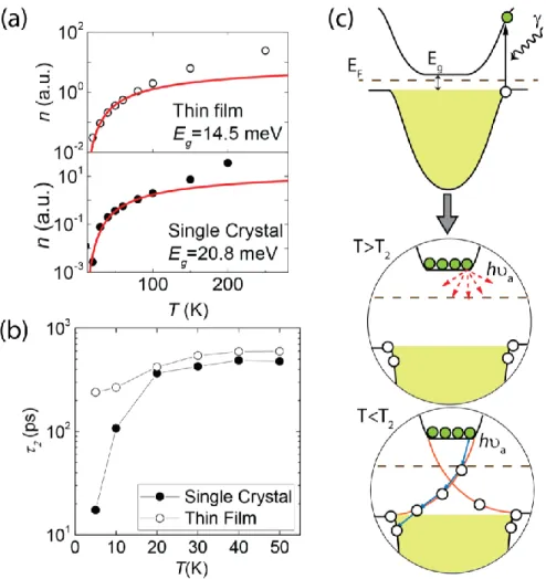
Due to the phonon bottleneck effect, a quasistationary photocarrier density (npc) is reached after the fast relaxation of hot electrons. Consistent with the RT model, profile of ∆R/R is strongly fluence dependent (Fig.S3 [32]). At low pump fluence when effects such as photocarrier induced band renormalization are minimized, maximum intensity (Imax) of ∆R/R is proportional to npc and also depends on the carrier density in thermal equilibrium (n) as: Imax ∝npc ≈ a/(1+bn), where a and b are constants relating to pump fluence and electron-phonon coupling strength. At low
temperatures, Imax increases dramatically (Fig.1), which is consistent with the reduction of thermal carrier density n. In the case of a narrow hybridization gap Eg, thermal carrier density n goes to zero at low temperature limit and can be expressed as a function of the temperature T as:
1/2
max( 0) / max( ) 1 exp( g / 2 )
nI T I T T E kT [29]. Figure 2(a) plots the temperature dependences of the so extracted thermal carrier densities in SmB6 single crystal and thin film samples. The data agrees with the model very well for the temperature window of 20 K – 100 K, suggesting a constant gap in that temperature range. Least square fitting yields a bandgap of 20.8 meV for single crystal and 14.5 meV for thin film, which agrees well with other reported values [19,22,38-40]. We note that the transport activation energy extracted from electrical measurements (Fig.S2 [32]) are considerably lower (9.2 meV for single crystal and 5.7 meV for thin film), which are likely biased by the mobility variance not included in the simple thermal activation fitting of the conductance.
Decay of ∆R/R can be fitted by a bi-exponential function with two decay constants 1 and
2 (1~ 100 ps,
2~ 102 ps). As predicted by the RT model, the fast decay time τ1 can be expressed as:
11
c n n
(2
pc)
, where c is a constant relating to electron-phonon coupling and high energy phonon decay rate [29,35]. At low laser fluence where npc n, thermal carrier density ndominates. This is consistent with the observed increase of τ1 as the temperature is lowered from 100 K to 20 K. The much longer decay time τ2, which is related toa slower relaxation process involving carrier diffusion and lattice cooling, remains unchanged in the temperature range of 20 K ‒ 100 K. Below 20 K, decay dramatically accelerates in the single crystal (Fig.1 (a)). Similar trend is also observed in the thin film but with a less significant change (Fig. 1(b)). This “anomaly” can be clearly visualized by temperature dependence of τ2 (Fig 2(b)), which exhibits more than one order of magnitude decrease below 20 K. RT model, designed for narrow bandgap systems, is clearly no longer applicable at these temperatures. The drastically different relaxation dynamics, however, can be explained considering the emerging of surface in-gap states (Fig. 2(c)). At higher temperatures, carrier relaxation is restricted by the “phonon bottleneck” caused by the zero density of states within the narrow energy gap. However, when in-gap states forms at the surface [10,17,19,22,23,41,42], “phonon bottleneck” is lifted. Surface in-gap states provide effective pathways for conduction band carriers to relax their energy (after diffusing to the surface) through multi-step scattering with acoustic phonons. This surface assisted carrier relaxation mechanism is very similar to the Shockley-Reed-Hall (SRH) process well-known in semiconductors [43,44], with the difference that typical SRH process is assisted by localized surface in-gap states instead. The carrier recombination rate (S) in SRH is determined by: S v nT s/n, where vT is the carrier thermal diffusion velocity and nsis the surface state density. In SmB6, the sharply increased surface state density ns below 20 K greatly enhances the recombination rate S and produces the significantly different reflectivity change time profile. We note that “overshoot” pass pre-excitation value is observed in the ∆R/R data at 5 K. Similar phenomena is also present in SRH processes with a large S [43,44]. Lattice heating can produce a change in reflectivity that is weaker but opposite to the effects of photocarriers. When photocarriers in the bulk diffuse toward the surface and relax to the valence band through the surface state, large amount of energy is “dumped”
to the lattice of the surface layer. The resultant significant surface heating can overpower the photocarrier effect, and thus explains the reflectivity signal “overshoot”. It is worth noting that the above discussed effect is observed only when the pump fluence is sufficiently low (Fig. S3 [32]). While laser heating is expected to play an important role, other factors that can potentially impact the surface states, such as pump produced thermal stress and the photocarrier related renormalization effects, should also be considered and are worth further investigation. Carrier relaxation in the thin film sample is slower comparing to the single crystal in all temperatures. We attribute this difference to the higher defect density and associated carrier trapping. This can also lead to reduced carrier diffusion speed and cause the less significant change of relaxation dynamics observed below 20 K.
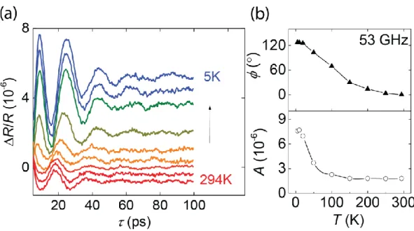
Overlapping on top of the monotonic decay, two types of coherent oscillation signals (S1, S2) are also observed in the time-resolved ∆R/R data. Terahertz level signal S1 is present in both single crystal and thin film samples, while the 53 GHz oscillations S2 is only found in the thin film. Both signals are heavily damped and exhibit little dependence on the laser polarization, probe pulse wavelength and the laser incidence angle.
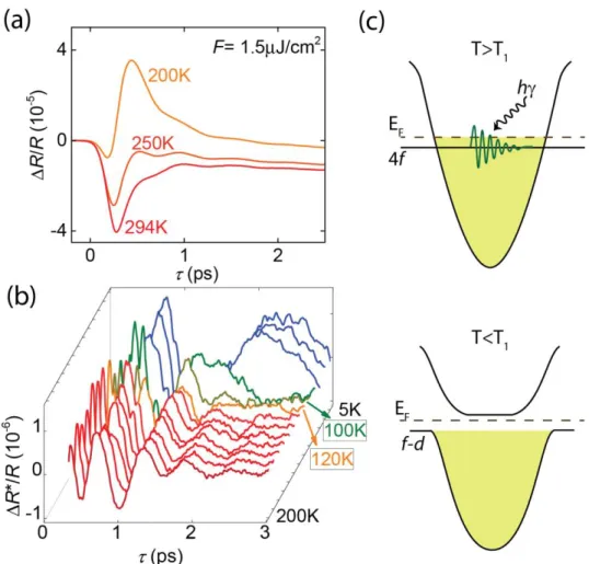
S1 oscillations in the single crystal has a frequency of 1.7 THz (Fig.3 (a)). Similar signal with a different frequency of 2.8 THz is observed in the thin film. To be concise, we focus the discussion on single crystal. After background subtraction, reflectivity changes associated with S1 at different temperatures are shown in Figure 3(b). Above 120K, S1 exhibits almost no temperature dependence. Though when the temperature is further reduced, decoherence abruptly occurs and S1 completely disappears at below 100K. The independence on probe wavelength and incidence angle requires S1 to be almost non-dispersive close to the zero wavevector. Optical phonons fit such description. However, 1.7 THz is substantially lower than all the known optical phonon branches [45-47]. Also, Raman phonon signatures are very similar in single crystal and thin film (Fig. S4 [32]), contradicting the observed S1 frequency difference. The strong temperature dependence also rule out defect related modes. Instead, we attribute S1 to the bulk plasma resonance of the strongly screened 4f heavy fermions (Fig.3(c)), of which a very close frequency (5.3 meV=1.3 THz) is reported by spectroscopy measurements [48]. Using the screened plasma frequency expression
2 *
4 / 0
p n ef m op
, effective mass m* 1000m0 and permittivity op 400 [48], 4f electron density of
n
4f
1.4 10
22 cm-3 can be calculated, which corresponds to approximately one electron per Sm atom. Time domain direct observation of 4f plasma oscillations provide a sensitive probe for the f-d hybridization taking place at low temperature. The decoherence of S1 starting at 120 K clearly indicates the onset of the hybridization process. As the heavy f electrons hybridize with the light d electrons, effective mass m* is expected to reduce significantly, resulting in an increased plasma frequency. As discussed previously, a bandgap of 20.8 meV opens at 100 K, at this point the greatly hardened plasma resonance (> 20.8 meV) merges into the interband electron-hole continuum and ceases to exist. The higher frequency observed in thin film is likely due to the reduced screening strength (smaller op) related to the presence of MgO substrate.A second damped oscillation S2 of much lower frequency (53GHz) is uniquely present in the thin film (Fig.1B, Fig.4A). We attribute S2 to the optically excited strain wave which reflects
repeatedly at the top and bottom surface of the film [49]. Surface absorption of the pump pulse induces a local thermal stress ( ) and initializes the strain wave propagating and reflecting inside the film. The resultant periodically changing strain at the film surface transiently induces changes in the local density of states (LDOS) and surface deformation, both resulting in the modulation of measured probe pulse reflection. Considering a model where the top surface of the film is free and the SmB6/MgO interface is fixed by the substrate, the expected oscillation frequency is f = v/4d [50], where v is the speed of sound in SmB6 and d is the film thickness (65nm). According to this formula, f = 53GHz corresponds to a sound speed of 1.4×10⁴ m/s in SmB6, which is high but reasonable given the well-known hardness of borides. While the frequency remains constant throughout the measurements, phase shift of S2 is observed upon cooling, which is owing to the variance of the ratio between stress induced changes in refractive index and extinction coefficient [49]. More interestingly,amplitude of S2 experiences a sharp upturn at 100 K. Based on a simple isothermal model, pump induced thermal stress can be expressed as 3(Q C/ )K, where Q
is the energy deposited by a single pump pulse, C is specific heat, β is thermal expansion coefficient and K is the bulk modulus. Since there is no evidence of discontinuous change of the involved parameters around 100 K [51,52]. The upturn in S2 amplitude is more likely due to the enhanced effect of stress on the local density of states at low temperatures, and possibly is related to the gap opening at 100 K. It has been reported that uniaxial stress (application of pressure) can effectively modulate the hybridization gap size [40,53,54]. With Q = 1×10⁶ Jm-3 and literature reported values of C = 4×10⁵ JK-1m-3 [52], β = -5×10⁻⁶ K-1 [51], K = 147 GPa [55], a rough estimation yields ~ 0.1 kbarat low temperatures, which is significant considering that a pressure larger than 40 kbar can suppress the gap completely[40,54]. We note that the thermal stress not only generate changes in the LDOS close to the Fermi level but may also impact the higher energy states, and the overall effects contribute to the change in 800nm probe’s reflectivity approaching 10-5 level at a pump fluence of 1.5μJ/cm2.
Conclusion
We have studied the transient carrier dynamics of SmB6 by femtosecond optical pump-probe experiments. Onset of f-d hybridization at 120 K and the band gap opening at 100 K is observed by monitoring the 4f heavy fermion plasma oscillations in time domain. Strain wave launched by the pump pulse is detected in the thin film. The sharp enhancement of the strain wave signal at 100 K provides further evidence of the gap opening. Between 100 K and 20 K, constant band gap energies of 20.8 meV and 14.5 meV are measured in bulk single crystal and polycrystalline film respectively. Below 20 K, dramatically accelerated carrier relaxation as well as significant surface lattice heating are detected. These phenomena can be well explained by the emergence of surface in-gap states and the resultant surface assisted carrier recombination process. Measurement results obtained in single crystal and thin film samples qualitatively agree with each other, strongly supporting the existence of a robust surface conducting layer at low temperature.
Acknowledgements
The work at West Virginia University is supported by the Department of Energy Grant No. DE-SC-0010399. The work at UC Irvine is supported by National Science Foundation grant DMR-1350122. The work at University of Wisconsin is supported by the National Science Foundation under DMREF Grant No. DMR-1234096.
References
[1] S.-c. Zhang, Physics 1, 6 (2008).
[2] L. Fu and C. L. Kane, Phys Rev B 76, 045302 (2007). [3] X. Wen and Q. Niu, Phys Rev B 41, 9377 (1990). [4] F. D. M. Haldane, Phys Rev Lett 61, 2015 (1988).
[5] K. Klitzing, G. DORDA, and M. Pepper, Phys Rev Lett 45, 494 (1980).
[6] M. Koenig, S. Wiedmann, C. Bruene, A. Roth, H. Buhmann, L. W. Molenkamp, X.-L. Qi, and S.-c. Zhang, Science 318, 766 (2007).
[7] D. Hsieh, D. Qian, L. Wray, Y. Xia, Y. S. Hor, R. J. Cava, and M. Z. Hasan, Nature 452, 970 (2008).
[8] Y. L. Chen et al., Science 325, 178 (2009).
[9] M. Dzero, K. Sun, P. Coleman, and V. Galitski, Phys Rev B 85, 045130 (2012).
[10] M. Dzero, K. Sun, V. Galitski, and P. Coleman, Physical Review Letters 104, 106408 (2010).
[11] Z. Fisk, J. L. Sarrao, S. L. Cooper, P. Nyhus, G. S. Boebinger, A. Passner, and P. C. Canfield, Physica B 223-224, 409 (1996).
[12] V. Alexandrov, M. Dzero, and P. Coleman, Phys Rev Lett 111, 226403 (2013). [13] H.-Z. Lu and S.-Q. Shen, Phys Rev B 84, 125138 (2011).
[14] S. Wolgast, Ç. Kurdak, K. Sun, J. W. Allen, D.-J. Kim, and Z. Fisk, Phys Rev B 88, 180405 (2013).
[15] D. J. Kim, S. Thomas, T. Grant, J. Botimer, Z. Fisk, and J. Xia, Sci. Rep. 3 (2013).
[16] X. Zhang, N. P. Butch, P. Syers, S. Ziemak, R. L. Greene, and J. Paglione, Phys. Rev. X
3, 011011 (2013).
[17] S. Rößler, T.-H. Jang, D.-J. Kim, L. H. Tjeng, Z. Fisk, F. Steglich, and S. Wirth, Proceedings of the National Academy of Sciences 111, 4798 (2014).
[18] W. Ruan, C. Ye, M. Guo, F. Chen, X. Chen, G.-M. Zhang, and Y. Wang, Physical Review Letters 112, 136401 (2014).
[19] M. Neupane et al., Nat Commun 4 (2013). [20] G. Li et al., Science 346, 1208 (2014). [21] N. Xu et al., Phys Rev B 88, 121102 (2013). [22] J. Jiang et al., Nat Commun 4 (2013).
[23] D. J. Kim, J. Xia, and Z. Fisk, Nat Mater 13, 466 (2014).
[24] S. Thomas, d. J. Kim, S. B. Chung, T. Grant, Z. Fisk, and J. Xia, arXiv:1307.4133 (2013). [25] D. H. Torchinsky, F. Mahmood, A. T. Bollinger, I. Božović, and N. Gedik, Nat Mater 12,
387 (2013).
[26] C. W. Luo et al., Physical Review Letters 108, 257006 (2012).
[27] T. Mertelj, V. V. Kabanov, C. Gadermaier, N. D. Zhigadlo, S. Katrych, J. Karpinski, and D. Mihailovic, Physical Review Letters 102, 117002 (2009).
[28] S. G. Han, Z. V. Vardeny, K. S. Wong, O. G. Symko, and G. Koren, Physical Review Letters 65, 2708 (1990).
[29] J. Demsar, V. K. Thorsmølle, J. L. Sarrao, and A. J. Taylor, Physical Review Letters 96, 037401 (2006).
[30] K. H. Ahn, M. J. Graf, S. A. Trugman, J. Demsar, R. D. Averitt, J. L. Sarrao, and A. J. Taylor, Physical Review B 69, 045114 (2004).
[31] J. Demsar, R. D. Averitt, K. H. Ahn, M. J. Graf, S. A. Trugman, V. V. Kabanov, J. L. Sarrao, and A. J. Taylor, Physical Review Letters 91, 027401 (2003).
[32] See Supplemental Material at... for the details in sample preperation and plots of transport measurement data, flence dependecne and Raman spectrum. .
[33] A. Rothwarf and B. N. Taylor, Physical Review Letters 19, 27 (1967).
[34] J. Demsar, R. D. Averitt, A. J. Taylor, V. V. Kabanov, W. N. Kang, H. J. Kim, E. M. Choi, and S. I. Lee, Physical Review Letters 91, 267002 (2003).
[35] V. V. Kabanov, J. Demsar, and D. Mihailovic, Physical Review Letters 95, 147002 (2005). [36] D. Talbayev et al., Physical Review Letters 104, 227002 (2010).
[37] U. Bockelmann and G. Bastard, Physical Review B 42, 8947 (1990).
[38] K. Flachbart, K. Gloos, E. Konovalova, Y. Paderno, M. Reiffers, P. Samuely, and P. Švec, Physical Review B 64, 085104 (2001).
[39] B. Gorshunov, N. Sluchanko, A. Volkov, M. Dressel, G. Knebel, A. Loidl, and S. Kunii, Physical Review B 59, 1808 (1999).
[40] J. C. Cooley, M. C. Aronson, Z. Fisk, and P. C. Canfield, Physical Review Letters 74, 1629 (1995).
[41] T. Takimoto, Journal of the Physical Society of Japan 80, 123710 (2011).
[42] F. Lu, J. Zhao, H. Weng, Z. Fang, and X. Dai, Physical Review Letters 110, 096401 (2013). [43] A. J. Sabbah and D. M. Riffe, Journal of Applied Physics 88, 6954 (2000).
[44] A. J. Sabbah and D. M. Riffe, Physical Review B 66, 165217 (2002).
[45] P. A. Alekseev, A. S. Ivanov, V. N. Lazukov, I. P. Sadikov, and A. Severing, Physica B: Condensed Matter 180–181, Part 1, 281 (1992).
[46] P. A. Alekseev et al., EPL (Europhysics Letters) 10, 457 (1989).
[47] P. Nyhus, S. L. Cooper, Z. Fisk, and J. Sarrao, Physical Review B 52, R14308 (1995). [48] G. Travaglini and P. Wachter, Physical Review B 29, 893 (1984).
[49] C. Thomsen, H. T. Grahn, H. J. Maris, and J. Tauc, Physical Review B 34, 4129 (1986). [50] C. Thomsen, J. Strait, Z. Vardeny, H. J. Maris, J. Tauc, and J. J. Hauser, Physical Review
Letters 53, 989 (1984).
[51] D. Mandrus, J. L. Sarrao, A. Lacerda, A. Migliori, J. D. Thompson, and Z. Fisk, Physical Review B 49, 16809 (1994).
[52] W. A. Phelan, S. M. Koohpayeh, P. Cottingham, J. W. Freeland, J. C. Leiner, C. L. Broholm, and T. M. McQueen, Physical Review X 4, 031012 (2014).
[53] J. Derr, G. Knebel, D. Braithwaite, B. Salce, J. Flouquet, K. Flachbart, S. Gabáni, and N. Shitsevalova, Physical Review B 77, 193107 (2008).
[54] S. Gabáni, E. Bauer, S. Berger, K. Flachbart, Y. Paderno, C. Paul, V. Pavlík, and N. Shitsevalova, Physical Review B 67, 172406 (2003).
[55] Sandeep, M. P. Ghimire, D. P. Rai, P. K. Patra, A. K. Mohanty, and R. K. Thapa, Journal of Physics: Conference Series 377, 012084 (2012).
Figure 1 Temperature dependence of the time-resolved pump induced (PI) reflectivity measured inSmB6 (a) bulk single crystal and (b) thin film. A low laser fluence 0.1 μJ cm−2 is used in the measurements.
Figure 2 (a) Thermal carrier densities extracted from the maximum amplitudes of PI reflectivity change signals (
R R
/
) plotted as a function of the temperature. Fitting of 1/2 Eg/2kTnT e is
performed to obtain the gap energies Eg. (b) Temperature dependence of the slow relaxation constant (τ2), extracted from bi-exponential decay fitting of PI reflectivity change (
R R
/
). (c) Illustration of the “phonon bottleneck” phenomena induced by the narrow hybridization gap aboveFigure 3: PI reflectivity measurement of single crystal at high temperatures, showing a 1.7 THz oscillation signal (S1). (b) Background subtraction is performed to emphasize the temperature dependence of the oscillating features. (c) Illustration of hybridization driven band gap opening. At temperatures above T1 = 120K, S1 can be optically excited and is associated with the 4f heavy electron plasma resonance. Below 120K, plasma mode is altered by the hybridization with light d
band electrons. Below 100 K, plasma oscillations are subject to interband Landau damping and cease to be detectable.
Figure 4: (a) Temperature dependence of the 53 GHz strain wave induced oscillations extracted from the PI reflectivity measurements of the thin film. (b) Amplitude of the oscillations sharply increases at 100 K and the phase gradually varies with the change of temperature. Pump fluence of 1.5μJ/cm2 is used in the measurements.
Ultrafast observation of electron hybridization and in-gap surface states
formation in Kondo insulator SmB6: Supplementary Information
Sanjay Adhikari1, Yanjun Ma3, Zach Fisk2, Jing Xia2, Chang-Beom Eom3, Cheng Cen1* 1Department of Physics and Astronomy, West Virginia University, Morgantown, West Virginia26506, USA
2 Department of Physics and Astronomy, University of California, Irvine, California
92697-4575, USA
3Department of Material Science and Engineering, University of Wisconsin-Madison, Madison,
Wisconsin 53706, USA
*Correspondence to [email protected]
Sample synthesis
SmB6 single crystals were grown using the aluminum flux method. These crystals are then inspected using X-ray analysis to make sure SmB6 is the only content. To further ensure that there is no remaining aluminum inside the crystal, we perform susceptibility measurements to check any sign of superconductivity of aluminum. The surfaces of these crystals were carefully etched using hydrochloric acid (50 HCL + 50 DI water) for 2 minutes and then cleaned using solvents to remove possible oxide layer. Samples used in the experiments have naturally existing well defined (100) surfaces that are a few mm in size. We have carried out transport measurements of crystals grown from the same batch and make sure there is low temperature resistance saturation, a sign of surface-dominated conduction.
Thin film of SmB6 is synthesized by pulsed laser deposition (PLD). A KrF excimer laser outputs 248 nm laser pulses, which is focused on a SmB6 ceramic target with the spot size of 2.8 cm2 in the deposition chamber. The laser repetition rate is 10 Hz, and the energy density is 3.6 J/cm2. The ablated SmB6 materials deposit on a MgO (100) single crystal substrate, of which the surface is polished and the temperature is kept at 850 C. The working distance is 6 cm. The growth pressure is maintained at 1 × 10⁻⁷ Torr during the deposition. Right after growth, X-ray diffraction on the film reveals its polycrystalline structure; however, it is also noticed that the film changes to amorphous phase over time even when it’s stored in a desiccator inside which the temperature is set to be about 20 °C and the humidity is controlled around 10%.
Transport Measurements:
Figure S1: Resistivity vs temperature for both (a) single crystal and thin film. Resistivity measurement for the single crystal was done in hall bar configuration and thin film was done in van der pauw configuration. The resistivity saturates at temperatures below 4K, consistent with the existence of surface conducting states. (b) Sheet carrier density and mobility as a function of temperature for the single crystal extracted from the hall voltage measurement.
Figure S2: ln() vs. 1/T, 20K<T<50K, for
single crystal (on the top) and thin film (on the bottom), where is conductivity. The fit, shown in red, is done using thermal activation law equation given by
0
( )T exp( Eg / 2kT)
. Where, k is the Boltzmann constant, and Eg is the energy gap.
Fluence dependence in pump probe measurements:
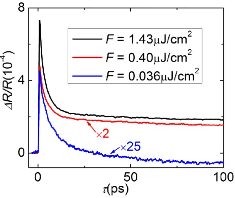
Figure S3: Pump induced reflectivity measurement for single crystal at 5K as a function of the pump fluence. In order to compare the three fluence conditions, values of the red curve are multiplied by 2 and blue by 25.
Raman Measurements
Figure S4: Room temperature Raman spectra from thin film and the single crystal. Both thin film and single crystal show the three main Raman active phonon modes of A1g (1263 cm-1), Eg (1128 cm-1) and T
2g (706 cm-1) symmetry (P. Nyhus et. al., 1997). These modes are associated with the displacement of boron atoms in SmB6. There is one major unknown mode at 979 cm-1.This mode, present in both thin film and single crystal, could be arising from residual photoresist after photolithography process (E. O. Potma et, al., 2004). All of the major Raman active modes in thin film sample are shifted, with less than 10%, to lower wavenumber. This could be due to the possible stress in the thin film and other crystalline quality related reasons.