2015 EOS/ESD Symposium, Reno, NV, Sept. 24-Oct. 2, 2015
Low Impedance Contact CDM
Nathan Jack and Timothy J. Maloney
Intel Corporation, 2501 NW 229th Ave., Hillsboro, OR 97124 USA e-mail: [email protected]
This paper is co-copyrighted by Intel Corporation and the ESD Association
Abstract – Relay-based contact CDM (CCDM) is shown to closely replicate the waveforms and failure currents of legacy field-induced CDM when the effective system impedances are approximately matched. The repeatability of the waveforms will be crucially important as CDM test levels decrease below 250 V. Recommendations for inclusion in future standards are presented.
I. Introduction
In an effort to replicate the stress conditions present in an automated manufacturing environment, the standardized field-induced CDM tester (FICDM) [1] relies on an air spark to generate the ESD event. The air spark is inherently variable and dependent upon many factors. The result is a “standard” which produces significant zap-to-zap variation [2]. To-date this variation has been tolerated as a necessary tradeoff to avoid the negative consequences that often accompany alternative test methods, such as the parasitic capacitance of socketed CDM [3].
When testing below the widely adopted qualification level of 250 V, FICDM variability transitions from inconvenient to intolerable. Figure 1 shows the maximum to minimum difference in Ipeak (top) and the
standard deviation (bottom) as a percentage of the average Ipeak of 50 zaps to calibration coins. Below
250 V, the variation in Ipeak as a percentage of the
mean increases as the precharge voltage Vpre
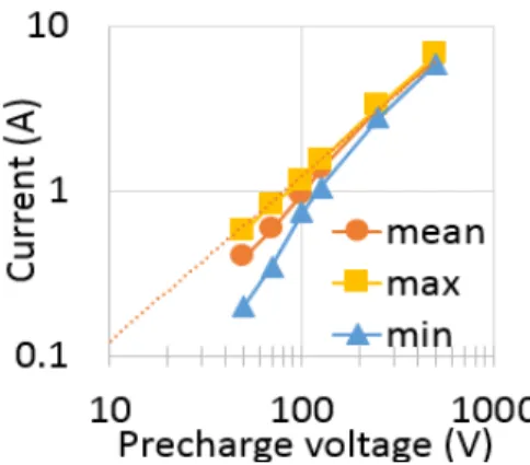
decreases. The data in Figure 2 reveal that while the maximum Ipeak is linearly proportional to Vpre, the
minimum Ipeak is not. Runt pulses are increasingly
common and the attenuation more severe as the Vpre
decreases, which in turn decreases the mean.
To satisfy scaling and circuit performance demands of the near future, components designed for less than 250 V CDM will become commonplace [4], [5]. The CDM protection levels for non-exposed intra-package I/Os (e.g., through-silicon vias) is likely to be well below 100 V CDM [5]. A repeatable, reproducible alternative to FICDM must be adopted to prevent a significant increase in the testing and design time wasted to accommodate a highly variable standard.
Figure 1: Ipeak maximum - minimum (top) and the standard deviation (bottom) of 50 zaps to JEDEC calibration coins as a percentage of the mean; 26% relative humidity. Data taken on an Orion2 FICDM system using an 8 GHz oscilloscope.
2
Relay-driven contact CDM testers (CCDM) such as capacitively coupled TLP (CC-TLP) [6] and Thermo Fisher’s “CDM2” [2] have been proposed to eliminate the air spark and improve repeatability. However, the decay constant of these 50 Ω systems results in pulses wider than those of FICDM, introducing a potential source of miscorrelation as will be shown. The rise time trise of CCDM can also be significantly faster
than FICDM [2] and can cause a miscorrelation in ICs where rise-time-sensitive protection devices are used (e.g., SCRs).
In this work, CCDM testers with reduced system impedance are presented. The new testers generate waveforms more closely resembling those of FICDM than their 50 Ω predecessors. Equivalent RLC models for the various testers are produced and compared. Failure correlation from a 14nm bulk finFET test chip containing various I/O types and protection devices is presented. Finally, a proposal is made for accommodating CCDM testers in future revisions of the CDM standard.
II. CCDM Tester Variations
CDM testers can be well approximated as an equivalent series RLC circuit [7]. The pulse width is an increasing function of the effective discharge resistance Reff and capacitance Ceff. The Reff of
existing 50 Ω CCDM testers will nearly always exceed that of FICDM, which can be as low as 24 Ω [7]. Consequently, reducing the system impedance of CCDM should result in better waveform matching to FICDM.
In this section, CCDM testers with system impedances of 50 Ω, 25 Ω, and 11 Ω are described.
A. 50 Ω CCDM
To-date, package-level 50 Ω CCDM has been instantiated in two primary forms: CC-TLP [6] and CDM2 [2]. Both are reviewed briefly here.
CC-TLP, illustrated in Figure 3, is essentially a 50 Ω VF-TLP tester with an FICDM-like test head. The VF-TLP pulse is applied at the pogo pin; the return path is the effective capacitance of the device under test (DUT) to the ground plane. A bipolar stress is delivered as displacement current charges and discharges the DUT during the pulse rising and falling edges, respectively. The current is extracted from the incident (Vinc) and reflected (VDUT) voltage
waveforms as in TDR VF-TLP:
𝐼𝐷𝐷𝐷(𝑡) = 𝑉𝑖𝑖𝑖(𝑡)−𝑉𝐷𝐷𝐷(𝑡)
50Ω . (1)
Figure 3: 50 Ω CC-TLP tester. The field plate resistor is not present in existing CC-TLP literature, but it can be added (as is done in CDM2) to more closely mimic the FICDM system.
CDM2 is illustrated in Figure 4. With the pogo pin contacting the DUT, the effective CDUT and the
coaxial cable leading to it are slowly charged. A relay then quickly discharges the system to ground through a 50 Ω coaxial cable and oscilloscope channel. This generates a unipolar current stress in the DUT. The current extraction is the same as for CC-TLP; see Equation (1). Vinc is the discharge with no DUT, and
VDUT is the discharge when contacting the DUT.
Figure 4: 50 Ω “CDM2” tester used in this work, as in [2].
Fundamentally CC-TLP and CDM2 are the same: both utilize a 50 Ω relay and transmission line to charge and/or discharge the device. Consequently the RC decay constant of the discharge to a given DUT is the same for both testers, provided the dimensions of the test head and field plate are the same.
3
B. 25 Ω CCDM
The system impedance of CCDM can be halved by connecting a parallel 50 Ω coaxial cable to the discharge path. This is illustrated in Figure 5. The system resembles a TDT VF-TLP system [8] whose pulse is applied to a CDM test head. A 200ps trise filter
is used to achieve a trise comparable to that of FICDM
– an advantage over CDM2. Similar to CC-TLP, displacement current stresses the device on the pulse rising and falling edges. To enable unipolar stress, the charge cable is terminated with an RC network. R is chosen to be 50 Ω to suppress reflections, and C is set to 10 nF. The resulting 500 ns RC time constant is slow enough to eliminate any significant displacement current in the DUT during the pulse falling edge.
Figure 5: Illustration of the 25 Ω CCDM tester used in this work, which resembles a TDT VF-TLP system injecting into a CDM test head. The RC termination of the charge cable ensures a single-polarity stress.
The device current extraction is similar to that of a TDT VF-TLP system (see Appendix A for more on IDUT extraction). From transmission line theory,
𝐼𝐷𝐷𝐷(𝑡) =𝑉𝑖𝑖𝑖(𝑡)−𝑉𝑟𝑟𝑟𝑟𝑟𝑖𝑟𝑟𝑟(𝑡)−𝑉𝑟𝑟𝑡𝑖𝑡𝑡𝑖𝑟𝑟𝑟𝑟(𝑡)
50Ω . (2)
Vtransmitted is the voltage measured directly at the
oscilloscope when in contact with the DUT. Vinc can
also be measured at the oscilloscope when the pogo pin is separated from the DUT. By observing that
𝑉𝑡𝑡𝑡𝑡𝑡𝑡𝑡𝑡𝑡𝑡𝑡(𝑡) =𝑉𝑡𝑡𝑖(𝑡) +𝑉𝑡𝑡𝑟𝑟𝑡𝑖𝑡𝑡𝑡(𝑡) , (3)
Equation (2) simplifies to
𝐼𝐷𝐷𝐷(𝑡) =𝑉𝑖𝑖𝑖(𝑡)−𝑉𝑟𝑟𝑡𝑖𝑡𝑡𝑖𝑟𝑟𝑟𝑟(𝑡)
25Ω . (4)
C. 11 Ω CCDM
The CCDM system impedance can be further reduced to below 25 Ω. One approach would be to add a third, fourth, or even fifth coaxial cable in parallel with the two that lead to the pogo pin in the 25 Ω system. As long as each is terminated with 50 Ω, the system impedance seen by the device is equal to 50 Ω divided by the total number of cables. Alternatively, a surface mount resistor can be soldered across the center and ground conductors near the pogo pin. In this work, a 20 Ω resistor with low parasitics is used. This is illustrated in Figure 6. The tester is otherwise identical to the 25 Ω system in Figure 5. The effective system impedance is now 20 || 50 || 50 Ω = 9/100 Ω = 11.11 Ω.
Figure 6: Zoomed-in illustration of 11 Ω CCDM. The tester is identical to 25 Ω CCDM with the addition of a 20 Ω surface mount resistor soldered across the center and shield conductors near the pogo pin.
The device current is as in Equation (2), with an additional 20 Ω path that must be accounted for:
𝐼𝐷𝐷𝐷(𝑡) =𝑉𝑖𝑖𝑖(𝑡)−𝑉𝑟𝑟𝑟𝑟𝑟𝑖𝑟𝑟𝑟(𝑡)−𝑉𝑟𝑟𝑡𝑖𝑡𝑡𝑖𝑟𝑟𝑟𝑟(𝑡)
50Ω
−𝑉𝑟𝑟𝑡𝑖𝑡𝑡𝑖𝑟𝑟𝑟𝑟(𝑡)
20Ω . (5)
By substituting Equation (3), Equation (5) becomes
𝐼𝐷𝐷𝐷(𝑡) =4∙𝑉𝑖𝑖𝑖(𝑡)−9∙𝑉𝑟𝑟𝑡𝑖𝑡𝑡𝑖𝑟𝑟𝑟𝑟(𝑡)
100Ω . (6)
Unlike 25 Ω CCDM, the waveform measured at the oscilloscope with the pogo separated from the DUT is not Vinc. Rather, it is a reference waveform Vrfr :
𝑉𝑡𝑟𝑡 =𝑉𝑡𝑡𝑖(1 +𝛤). (7)
In Equation (7), Γ is the reflection coefficient for the incident pulse when it reaches the 20 || 50 Ω branch. By substituting Equation (7) into (6), one obtains
𝐼𝐷𝐷𝐷(𝑡) =9∙𝑉𝑟𝑟𝑟(𝑡)−9∙𝑉𝑟𝑟𝑡𝑖𝑡𝑡𝑖𝑟𝑟𝑟𝑟(𝑡)
100Ω
= 𝑉𝑟𝑟𝑟(𝑡)−𝑉𝑟𝑟𝑡𝑖𝑡𝑡𝑖𝑟𝑟𝑟𝑟(𝑡)
4
III. Discharge Waveform Analysis
In this section, discharge waveforms from the three CCDM systems described in Section II are compared against FICDM. All three CCDM systems were implemented using modifications of the CDM2 Orion2 tester by Thermo Fisher [2]. All physical dimensions of each tester (e.g., ground plate size and field plate dielectric) conform to the JEDEC standard [1]. An 8GHz oscilloscope was used for all waveform measurements in this work.
A. Waveform Comparison
Discharge waveforms from FICDM and CCDM zaps to JEDEC calibration coins are shown in Figure 7. As expected, CCDM more closely replicates FICDM when the system impedance is reduced. Only the 11 Ω CCDM system can generate an underdamped waveform on both coins like FICDM. The pulse base width of the 50 Ω discharge is significantly wider than that of the legacy tester, especially when zapping the larger coin.
Figure 7: Discharge waveforms from FICDM and CCDM zaps to JEDEC large and small calibration coins.
Put another way, the total charge Qtot delivered for a
given Ipeak increases with the system impedance. This
is shown in Figure 8, where Ipeak is plotted as a
function of Qtot using four calibration coins of
different sizes. In the case of the largest coin, the Qtot
per Ipeakis more than double that of FICDM. The 25 Ω
system comes closer to approximating FICDM, while
the 11 Ω system matches quite well. For the smallest coin, the discharge from the 11 Ω system actually has slightly less charge per Ipeak than FICDM. This
suggests that a slightly larger system impedance – like 16 Ω – might result in the best overall match.
Figure 8: Total charge delivered to obtain a given Ipeak when stressing four calibration coins of different size.
It has been proposed that the pulse width of a 50 Ω CC-TLP system could be artificially reduced by applying, for example, a 1 ns VF-TLP pulse to the system rather than a 10 – 20 ns pulse. While this would limit the duration of the stress associated with the VF-TLP pulse rising edge, it also makes the pulse width approximately independent of CDUT. This is
undesirable if CCDM is to replicate FICDM; the latter clearly exhibits pulse width dependence on CDUT (see
Figures 7 – 8). Low impedance CCDM can capture this CDUT dependence and replicate the legacy Qtot per
Ipeak.
B. System RLC models
Equivalent 2-pole RLC models derived from the discharge waveforms can lend significant insight into waveform correlation with FICDM [7]. The models derived from the waveforms in Figure 7 are listed in Table 1. The Ceff for a given coin is constant across
testers – the required outcome since all testers use the same field and ground plates. The commercial FICDM test head contained a ferrite disk (not prohibited in the 2013 JEDEC standard [1]), while CCDM uses no ferrites. This results in a lower inductance Leff for CCDM in all cases [7].
5
The primary differentiator among the testers is Reff,
the largest component of which is the characteristic impedance of the system. The Reff of 50 Ω CCDM
with the large coin is more than three times that of FICDM, resulting in a wide discharge pulse. The excellent waveform match of 11 Ω CCDM to FICDM is primarily due to the close agreement of Reff. Table 1
also indicates that the dependence of Reff on coin size
(i.e. CDUT) is opposite between FICDM and CCDM:
Reff decreases with CDUT for CCDM while the reverse
is true for FICDM. So, while the Reffof 11 Ω CCDM
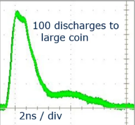
matches FICDM for the large coin, it is somewhat low for smaller DUTs. This further supports the idea that a CCDM system impedance somewhere between 11 Ω and 25 Ω would likely result in the best overall fit. Because CCDM is mercury-relay driven, the repeatability is excellent, as shown in Figure 9 for the 25 Ω system.
Figure 9: Waveforms of 100 discharges to the large calibration coin using 25 Ω CCDM.
C. Ipeak dependence on Vpre and Ceff
The Ipeak generated for a given power supply voltage
Vpre varies significantly among the testers, as shown
in Figure 10. FICDM generates at least twice as much current per Vpre than the CCDM testers. This is due to
differences in the stress generation methods.
Figure 10: Ipeak for a given Vpre when stressing the large JEDEC coin.
During FICDM, the potential of the DUT is nearly equal to Vpre just before the spark pulls it to ground
potential; i.e., nearly the full Vpre generates the current
stress. This is not the case for CCDM. Vpre is applied
initially to the charge cable (terminated by CDUT in 50
Ω CDM2). When the relay closes, Vpre is divided
equally across the two 50 Ω coaxial cables on either side of the relay. This results in a square pulse of amplitude Vpre / 2 that travels away from the charge
cable, and a -Vpre / 2 pulse that travels towards the end
of the charge cable. In CDM2 the -Vpre / 2 pulse in the
charge cable is superimposed upon the static Vpre that
was initially present across CDUT. In CC-TLP and 25
Ω – 11 Ω CCDM, the Vpre / 2 pulse travels towards
the DUT. In other words, in both CDM2 and CC-TLP-type systems it is the transition from Vpre to Vpre /
2 across CDUT that initiates the current stress (see
Appendix A for further discussion). This is approximately half of the voltage involved in the FICDM stress generation and hence generates approximately half the Ipeak of FICDM. In the 25 Ω
and 11 Ω case, the current from the Vpre / 2 pulse is
further diverted from the DUT to ground through the additional parallel paths connected near the pogo pin (see Figures 5 and 6). Hence, the IDUT per Vpre is even
lower in these systems than in 50 Ω CCDM.
Ipeak is also a function of the device capacitance;
however, this dependency is not the same between FICDM and CCDM. As shown in Figure 11, FICDM Ipeak is more strongly modulated by Ceff than is
CCDM. This means that while Vpre can be adjusted to
match the Ipeak of CCDM to FICDM for a given Ceff,
this same Vpre will not produce a matched Ipeak for a
different Ceff.
Figure 11: Ipeak dependence upon Ceff for FICDM and 25 Ω CCDM. The data is from zaps to calibration coins of four different sizes at the FICDM equivalent of 250 V.
Given the different dependencies of Ipeak on Vpre and
Ceff, Ipeak must be used rather than Vpre to correlate the
6
IV. Test Chip Correlation
The testers discussed in Section II were used to stress the I/Os of a 14 nm bulk finFET [9] test chip. The test chip and the measurement results are discussed in this section.
A.
Test Chip Description and
Discharge Waveforms
The test chip utilizes dual diode protection at the I/Os with an RC triggered PMOS clamp between the power rails. Two different I/O architectures are used on the chip, and the sizes of the ESD diodes are varied. The test chip is packaged in a large 38 mm by 38 mm LGA package with heat sink. Because pulse width dependence is more pronounced with larger DUTs (see Figure 7), this large package should exacerbate any miscorrelation arising from pulse width. Indeed, the discharge waveforms from the test chip, shown in Figure 12, reveal a significant pulse width dependence on tester impedance. Trise is
approximately matched across the systems, though that of CDM2 is approximately 50 ps sharper than the others. Wafer-level characterization indicates these I/Os are not sensitive to trise, so any miscorrelation
should arise from differences in twidth.
Figure 12: Discharge waveforms from the test chip used in this work.
B.
Ipeak vs. Pin Location
While Qtot is independent of I/O pin location in the
package during FICDM testing, Ipeak and twidth are
location dependent [10]. Waveforms from pins near the center have a larger Ipeak and shorter twidth than
those from pins near the package edge (charge across the package must travel longer distances to reach an edge discharge point). This source of variation is an important one for CCDM to capture if it is to replicate FICDM failures.
The I/O peak currents measured during FICDM and CCDM are mapped by pin location in Figure 13. The
trend of larger Ipeak in the center vs. the edges holds
true for CCDM. This is an expected but important observation for ensuring correlation with FICDM Ifail.
Figure 13: Map of Ipeak by I/O pin location on both FICDM and CCDM taken at the FICDM equivalent of 250 V.
C.
I
failCorrelation
Three test chip samples per CDM tester type were stressed and the failure currents recorded for several pins. All testers were configured to generate positive current stress into the pin – the worst case stress condition for this test chip. Failure was defined as a 4% post-stress deviation in an unpowered IV sweep of the pin. Because the low impedance CCDM testers produce less Ipeak per Vpre than FICDM (see Figure
10), sufficient current could not be generated to cause failure in a few I/Os. Where failure was not achieved, the last passing current is reported.
The Ifail results are shown in Figures 14 and 15 for two
different I/O types. For both I/O types, the wider pulses of 50 Ω CCDM result in Ifail values
significantly below FICDM. Ifail for 25 Ω CCDM is
typically lower than FICDM, but within 5%. The Ifail
7
FICDM. As discussed in Section III, it is likely that even better waveform and failure correlation could be obtained with a system impedance somewhere between 25 Ω and 11 Ω. Regardless, either of the lower-impedance CCDM testers are excellent candidates for successors to FICDM.
Figure 14: Failure current correlation for I/O type #1.
Figure 15: Failure current correlation for I/O type #2.
V. Inclusion in Standards
Future CDM standards must allow the use of innovative FICDM alternatives such as CCDM. This can be achieved while preserving the legacy voltage classification levels, allowing both FICDM and CCDM to co-exist. If the following three properties of a tester match those of FICDM, the stress to the DUT should be identical:
Property 1: The distribution of charge across the DUT
Property 2: The Ipeak delivered during the stress
Property 3: The waveform shape, including rise time, pulse width, and charge per Ipeak
Property 1 above can be guaranteed by specifying all test head and field plate dimensions, including the pogo pin length and field plate dielectric. The characteristics in Property 3 should be specified in terms of acceptable ranges when stressing specific calibration coins.
To achieve Property 2, CDM hardness should be quantified in terms of Ipeak rather than Vpre (see
Section III.C). Vpre then becomes a legacy “test
condition” rather than an actual measure of the field plate voltage, much as is done in the recent Joint CDM Standard [11].
Mapping between Ipeak and the legacy Vpre can be
achieved through a look-up table or continuous model, with Vpre and Ceff as input variables. It was
shown in [7] that FICDM Ipeak can be very accurately
predicted with an RLC model. Leff is approximately
constant. The relationship between Reff and Ceff is
linear:
𝑅𝑡𝑟𝑟∙ 𝐶𝑡𝑟𝑟 =𝑅0∙ 𝐶𝑡𝑟𝑟+𝑡𝑡𝑡0. (9)
The constants R0 and tau0 are chosen empirically,
leaving Ipeak as a function of only two variables: Vpre
and Ceff. This is illustrated in Figure 16, where the
excellent fit to measurements on various calibration coins can be seen. The maximum Ipeak rather than the
average was used; arguably CCDM should be targeted to replicate the worst stress a device pin could feel on FICDM. This also simplifies the modeling since, for a given Ceff, the maximum Ipeak is linear with Vpre while
the average is not (see Figure 2).
8
A CCDM test flow like the one proposed below would capture the dependencies embedded in the legacy FICDM voltage qualification levels:
1. Zap the VSS pin of the largest domain on the
product. Software integrates this waveform to determine Ceff automatically.
2. To test a part for a given Vpre robustness (e.g.
“200 V CDM”), the Ceff from Step 1 is plugged
into the continuous FICDM model of Figure 16 to obtain the targeted Ipeak. Using the known Ipeak per
Vpre relationship of the CCDM tester for that Ceff,
software automatically sets Vpre to achieve the
Ipeak specified as per Figure 16.
3. With Vpre now established, all pins are stressed.
Ipeak variation by pin location occurs naturally (an
essential part of Property 2).
4. The results can either be reported in terms of legacy Vpre or Ipeak, regardless of whether an actual
FICDM tester or a CCDM tester was used.
VI. Conclusions
Future CDM standards must allow the use of alternatives to FICDM. This will be especially crucial as qualification levels decrease below 250 V. A methodology for allowing co-existence of alternative testers with FICDM in future standards was presented. Such a standard will open the door for innovations in CDM tester design, the most promising of which is likely to be low impedance CCDM. The proposed methods for reducing the system impedance of CCDM result in excellent waveform and failure correlation to FICDM – a significant improvement over their 50 Ω predecessors. A broader correlation study involving multiple on-chip protection schemes, technology nodes, and IC suppliers should drive the ultimate selection of the CCDM system impedance adopted as an FICDM alternative.
Appendix A: Extracting CCDM
Device Currents
CCDM applies a step function to a matched transmission line with target load ZL at its end, as
pictured in Figure A.1. Current in the s-domain can be found from the input admittance at the step source, or . ) ( 1 ) coth( 1 2 0 0 0 0 s L e Z Z s V s sZ V t t − ⋅ + + + ⋅
= (A.1)
Figure A.1. Transmission line model of CCDM or CC-TLP.
The first term of the last expression is the TLP current into Z0 from an open circuited (ZL=∞) line [12], [13]
as in Fig. A.1, i.e., a calibration pulse. The second term is the current through ZL, which will at least
include the device current, and the exponential is the expected round-trip transmission line delay of 2t. The second term of (A.1), exclusive of delay, is the device current. This is true both for CC-TLP (Figure 3) in which the applied pulse charges the device, as well as CDM2 (Figure 4) in which the applied pulse
discharges the device. For charge-down, ZL=∞ at s=0
is required, as with series capacitance.
For low impedance CCDM (Figures 5-6), ZL should
be decomposed into two parts as in Fig. A.2: the removable device Zd(s), and the fixed Zp, which
includes a shunt resistor, if any, plus the exit transmission line (usually another Z0), in parallel with
the shunt resistor. The resistor and matched exit line preclude the charge-down mode, but enable a “through” pulse for measurement. Let this measured pulse be Vp, Ip, where Vp/Ip=Zp whether Zd(s) is
connected or not. Let the near-end (reflected) measured current be Im. Eq. (A.1) leads us to
(A.2)
where (A.3)
Similarly, transmitted current into Zp is
(A.4)
But also from current division, device current
(A.5) + + + ⋅ = ) sinh( ) cosh( ) sinh( ) cosh( 1 1 ) ( 0 0 0 0 s Z s Z s Z s Z Z s V s I L L t t t t ) sinh( ) cosh( ) sinh( ) cosh( ) ( 1 ) coth( 1 0 0 0 0 s s s s Z Z s V s sZ V
L t t
t t t + − ⋅ + + + ⋅ = . 0 0 0 Z Z Z Z Z p p
p = +
, )) ( )( ( ) ( ) ( 0 0 0 s Z Z Z Z s Z Z s V s I d p p d p
m + +
+ ⋅ = . )) ( )( ( ) ( ) ( 0 0 0 s Z Z Z Z s Z s V s I d p p d
p = ⋅ + +
). ( ) ( )) ( )( ( ) ( 0 0 0 s I s I s Z Z Z Z Z s V s
I m p
d p p
p
9 Figure A.2. Low-Z CCDM model; Zp represents through line and
shunt resistor.
Thus we have a way to measure device current with reflected and transmitted signals with the device in place. But what if we want to avoid setting up the reflection measurement Im? Again, Vp/Ip=Zp, but now
Vp is Vtransmitted from Sections II.B and II.C when Zd is
connected. Meanwhile, Vrfr from Section II.C is Vp
with no device, or
(A.6)
The coefficient of Vi is the transmission coefficient
and identical to (1+Γ) in Eq. (7). Ii=Vi/Z0. But
Im=Ii-Ir, thus Id=Ii-Ir-Ip (Ir being reflected current, and
Ir =Vr/Z0). However Vrfr=IrfrZp=Vr+Vi also.
Eliminating Ii and Ir from these equations gives
. )
1 )( (
0
0 p
d transmitte rfr
p p
rfr d
Z V V
Z Z I
I
I = − + = − (A.7)
This agrees with Eq. (8) in II.C. It can also be shown that
), 1 )( (
0
Z Z I
I
Id = m− rfr + p (A.8)
thereby allowing all-reflection measurements. Thus from (A.5), (A.7), and (A.8), any two of the quantities Im, Ip and Irfr are sufficient for determining Id, while all
three allow redundant self-checking of the setup. If Zp
is a shunt resistor Rx in parallel with exit line of
impedance Zt, then Zp=RxZt/(Rx+Zt), but usually
Zt=Z0.
References
[1] “Field-induced charge-device model test method for electrostatic discharge-withstand thresholds of microelectronic components,” JEDEC, Arlington, VA, USA, JESD22-C101F, 2013.
[2] R. Given, M. Hernandez, and T. Meuse, “CDM2 – A New CDM Test Method for Improved Test Repeatability and Reproducibility,” in Proc. EOS/ESD Symp., 2010, pp. 359-367.
[3] M. Chaine et al., “Investigation into socketed CDM Tester Parasitics,” in Proc. EOS/ESD Symp., 1998, pp. 301-310.
[4] Industry Council on ESD Target Levels. (2009, Mar.). White Paper 2: A case for lowering component level CDM ESD specifications and requirements. [Online]. www.esda.org/documents/IndustryCouncilWhitePaper 2.pdf.
[5] C. Duvvury, “CDM qualification: technology impact, testing nuances, and target levels,” presented at the International Electrostatic Discharge Workshop, Lake Tahoe, CA, 2015.
[6] H. Wolf, H. Gieser, W. Stadler, and W. Wilkening, “Capacitively coupled transmission line pulsing CC-TLP—A traceable and reproducible stress method in the CDM-domain,” in Proc. EOS/ESD Symp., 2003, pp. 338-345.
[7] T. Maloney and N. Jack, “CDM tester properties as deduced from waveforms,” in Proc. EOS/ESD Symp.,
2013, 9A.1. [Online]. Available: http://ieeexplore. ieee.org/stamp/stamp.jsp?tp=&arnumber=6635950. Expanded version also in IEEE Trans. Mat. Dev. Reliability, Vol. 14, no. 3, Sept. 2014, pp. 792-800. [8] E. Grund and R. Gauthier, “VF-TLP systems using
TDT and TDRT for Kelvin wafer measurements and package level testing,” in Proc. EOS/ESD Symp., 2004, pp. 338-345.
[9] S. Natarajan et al., “A 14nm Logic Technology Featuring 2nd-Generation FinFET Transistors, Air-Gapped Interconnects, Self-Aligned Double Patterning and a 0.0588µm2 SRAM Cell Size,” IEDM, 2014, #3.7.
[10] J. Di Sarro, B. Reynolds, and R. Gauthier, “Influence of package parasitic elements on CDM stress,” in Proc. EOS/ESD Symp., 2013, 9A.3.
[11] “Charged Device Model, Device Level,” ANSI/ESDA/ JEDEC, JS-002, 2014.
[12] T.J. Maloney, "Antenna Response to CDM E- fields", in Proc. EOS/ESD Symp., 2012, pp.269-278.
[13] T.J. Maloney, "Pulsed Hertzian Dipole Radiation and Electrostatic Discharge Events in Manufacturing", IEEE EMC Society Magazine, Q3/2013 issue, pp. 49-57.
. 2 ) (
2
) (
)
( 0
0 0
0
i p i p p
p p
rfr V Z I
Z Z
Z
Z Z
Z
s V s
V =


![Figure 16: Solid lines: a continuous 2-pole model [7] of FICDM I peak as a function of C eff and V pre , with L eff = 11 nH, tau 0 = 85 ps, and R 0 = 20 Ω](https://thumb-us.123doks.com/thumbv2/123dok_us/8195279.2172566/7.918.478.821.506.957/figure-solid-lines-continuous-model-ficdm-function-ω.webp)


