Stacked PMOS Clamps for High Voltage Power Supply
Protection
Timothy J. Maloney and Wilson Kan
Intel Corporation, SC12-607, 2200 Mission College Blvd., Santa Clara, CA 95052. Tel. (408)765-9389, e-mail: [email protected]
Abstract - Large PMOS FETs with multiple gates can be arranged to provide ESD protection to high voltage on-chip power supplies in submicron integrated circuits. These clamps divide the supply voltage among several gate oxides; the circuitry accompanying the large series FETs provides near-maximum gate drive during the ESD for high pulsed current. Layouts are densely packed because minimum dimensions can be used and because no contact is needed between the stacked gates. The designs for high voltage are extensions of the large PMOS FET ESD clamps and timed drive circuitry that are used to clamp ordinary on-chip power supply lines.
Introduction
In recent years, complementary metal-oxide-semiconductor field-effect transistor (CMOS FET) scaling, power supply voltage scaling, and FET engineering for performance have caused a continued need for ESD protection methods which can be easily applied to inputs and outputs, without interfering with process development. The preference has been to exploit devices that are available “for free” as part of the process, and which do not need to be engineered for ESD performance and then made compatible with other goals.
These protection methods focus on defining smooth ESD current paths through the chip for the possible ESD events in stress testing and in actual handling. On input and output pins, the natural diodes to power and ground are used whenever possible, and current paths are linked together with the help of power supply clamps [1-4]. The latest designs for power supply clamps in submicron technology take full advantage of device scaling, which only in recent years has made it possible to dissipate ESD-scale currents (on the order of amperes, but only for nanoseconds) within small amounts of chip area (bond pad size) using MOS FET conduction. In earlier days, some kind of avalanche breakdown event had to be used, but sensitivity to process and triggering events made these methods very difficult to execute. With dual diodes for basic inputs and outputs, and special p-channel MOS (PMOS) FET circuits for power supply linkage, smooth ESD current
paths can be defined for nearly all varieties of chip interface with the outside world. PMOS FET clamping methods for ESD have become important for all of our company’s low voltage deep submicron CMOS products. They also help to solve the ESD protection problem for mixed voltage products, where compatibility with signals from earlier technologies is desired.
This paper will focus on the PMOS power supply clamp, in particular the PMOS power clamp with stacked transistors, designed to stand off power supply voltages in excess of the ordinary Vcc of the process. Stacked PMOS FET clamp designs will be shown to be area-efficient and compatible with ESD design goals for mixed voltage supply products.
I. PMOS Power Supply Clamps
I.a. Design
The scaling of power supply voltages below 5 volts in recent years has meant that components need to be backward compatible, to some extent, with chips running on higher voltage supplies. Table 1 summarizes the situation with five typical CMOS integrated circuit (IC) processes of the past few years, with Proc1 being the last of the processes allowing a continuous 5V across the gate oxide.
Much work on the use of diodes for cross-linking similar power supplies has been reported [1-2]. Less obvious is how to clamp dissimilar power supplies, such as Vcc to Vss. These stand-alone power supply clamps also can solve the problem of powerup sequencing (as when “similar” Vccx power supplies are powered up and may overstress their crosslinking diodes) and have become increasingly popular as a result of their success.
5 V 3.3V 2.5V 1.8-2.0 V 1.3-1.5V
Proc1 (0.8 µm)
Proc1 low
Proc2 hi Proc2
(0.6 µm)
Proc3 hi+ Proc3 hi Proc3
(0.35 µm)
Proc4 hi++ Proc4 hi+ Proc4 hi Proc4
(0.25 µm)
Proc5 hi++ Proc5 hi+ Proc5 hi Proc5
(0.18 µm)
Table I. Compatibility of submicron CMOS technology; Proc1 is last 5V process.
Work at our company and others in the 1992-95 time frame pointed toward the need for power supply clamping in ESD protection, and toward the need for a design that would yield equivalent or better performance with each process generation. Our rigorous qualification standards required universal application of power clamp cells, meaning that each clamp should pass all standard ESD tests with some margin (>4-8kV human body model (HBM), >1.2kV socketed charged device model (CDM)) in stand-alone mode, so that an arbitrarily small power supply would be protected. In addition, pulsed I-V behavior must be consistent with sinking at least a 2kV HBM peak current (1.33 amps) below the known danger Vcc voltage for all ordinary circuits in the process, even vulnerable ones (it was expected that every supply would be designed with at least two clamps). These criteria, and the cost-driven desire not to add masks or tamper with the performance-engineered FET process, drove us away from n-channel MOS (NMOS) FET clamps [5,6] because the salicided devices, even large ones, failed miserably on all ESD tests. Unsalicided NMOS devices resembling some of Worley’s [6] had the same reported problems with size and CDM behavior. Instead we went with PMOS devices; the simplest of these will be called pmosclamp here.
The practice of using MOSFETs in ordinary conduction mode for ESD clamping of power supplies began with 0.8 µm technology [5,6], when MOSFET
current densities reached reasonable levels. More recently, MOSFETs have scaled to deep submicron dimensions in production CMOS integrated circuit (IC) technologies, and the current per unit area in the “on” state (gate drive at full power supply voltage) has reached even higher levels. These currents are higher still for the pulsed voltages that a typical power supply line can tolerate. Transistor dimensions have scaled such that, if desired, a pulsed one amp of current can be sunk by a MOSFET in an area far less than the size of one bond pad (104 µm2). With this capability, it is more efficient than ever to fabricate ESD power supply clamps with large MOSFETs and accompanying circuitry designed to drive the gates hard. We have preferred to use p-channel FETs for power clamps, as shown in Figures 1-4, and have found that they allow dense packing of gate stripes and contacts while maintaining substantial ESD immunity [2-4].
Vcc
T1
C1 T2
T3
C2
Figure 1. RC-timed circuit for PMOS FET power clamp (pmosclamp); T2 and C1 enhance gate drive.
Figure 2 shows transmission line pulsed (TLP, [8]) I-V curves [2,3] for a pmosclamp protection circuit as in Fig. 1. The “idealized” curve is from a test pattern with the T1 gate artificially hard-wired to Vss and shows how close we come to desired grounding of the gate during the pulse. Note that the I-V of a pmosclamp with an RC network only, without the optimized trigger circuit including C1 and T2, shows clearly degraded characteristics as the gate does not fully turn on. The gate length used in Fig. 1 matched for the three examples shown, and happened to be well above the process minimum. The pmosclamp now routinely used in products has about 10% higher pulsed current than shown and its gate length is still substantially above the process minimum. The subthreshold leakage of these pmosclamps is not an issue, and is below 1 µA until considerably above 100 C. The clamps were also shown to be robust against power supply noise, which was simulated on test chips with a high-frequency signal applied to the power supply node. There have been no reliability problems with the clamps on recent products.
Pulsed I-V
0.0 0.5 1.0 1.5 2.0 2.5 3.0
0 2 4 6 8 10
V(volts)
I (
Amps
) pmosclamp
idealized
RC only
Figure 2. Pulsed I-V behavior of pmosclamp in 0.25 µm process; idealized curve has T1 gate artificially grounded and RC only has no inverter driving the T1 gate.
I.b. Simulations and Tests
Simulations of these circuits (using the standard process MOSFET model) match the pulsed I-V curves almost perfectly to the device model’s voltage limit of 4-5V and the extrapolated model is still fairly close to measured data. Note in Fig. 2 how the pmosclamp continues to conduct (without destruction, for 100 nanosecond pulses) up to 9-10V, far beyond the observed dc punchthrough voltage, around 5-6V. 10V is also greater than the pulsed voltage where some other circuit on Vcc would fail. This is sometimes called the danger voltage, about 8V for this 0.25 µm
process. Thus the pmosclamp clearly will not be the first point of failure. The HBM self-protection of these clamps was measured to be 8 kV, and CDM did not fail to the limit of the 2kV KeyTek socketed tester. CDM product results are also very good.
I.c. Scaling of the PMOS clamp
The equivalent pmosclamp for the 0.35 µm process [9] has roughly the same I-V curve as in Fig. 2, and is in a still-reasonable 12,000 µm2, but this uses over 50% more area than the 0.25 µm process. On the other hand, for a 0.18 µm process [10], we have designed a pmosclamp in less than 5,000 µm2, yet it sinks almost twice as much pulsed current at 6V (3.1 amperes) as the pmosclamps for the 0.35 µm and 0.25 µm processes. The scaling trend definitely points in a favorable direction, and should continue until such MOS conduction of pulsed currents runs into thermal limits. All of this is because, with shorter FET channels, we can achieve more pulsed and dc current sinking per unit area as processes scale, and because current flow in PMOS FETs is uniform. In the old days of process feature size of 1.0 µm and above, the same PMOS FETs for sinking ESD currents would have been absurdly large; however just in the past few years, as these results show, it has become possible to sink more than an ampere of pulsed current through ordinary MOS conduction in a production PMOS FET less than the size of a bond pad. And while devices have scaled dramatically due to Moore’s Law, ESD events have not— the human being, source of the HBM, has not scaled noticeably (!), and while electronic packages, source of the CDM, have proliferated into a variety of sizes and shapes, the CDM event is roughly the same as always. Thus device scaling once again teaches us to be on the lookout for opportunities as well as drawbacks.
II. High-Voltage PMOS Clamps
II.a. 0.25
µ
m process, 2-stack
The design and performance of clamps in Figs. 1-4 are described in greater detail in Refs. 2 and 3.
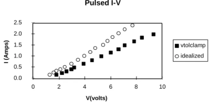
Figure 4 [2,3] shows a TLP I-V curve for the voltage-tolerant clamp (vtolclamp) of Figure 3 for a 0.25 µm process as described above. The “idealized” curve shows the pulsed I-V with the midpoint (as in Fig. 3) artificially grounded. This shows that there is room for improvement in the gate drive circuitry, which tries to ground the T1 and T2 gates during the pulse so that maximum current sinking is achieved until RC timeout. But performance is adequate. Also, no failure of the device on TLP up to a sustained 10V, 100 nsec was observed, so again some other circuit on the power supply is expected to fail before the hi-V power clamp (although the pulsed danger voltage for hi-V circuits is not exactly known). HBM and CDM did not fail up to the limits of the KeyTek Zapmaster tester, 8kV and 2kV, respectively.
hi-Vcc
T1
C1 T2
T3
T4
T5
midpoint
C2
Figure 3. PMOS power supply clamp for up to twice nominal Vcc.
Pulsed I-V
0.0 0.5 1.0 1.5 2.0 2.5
0 2 4 6 8 10
V(volts)
I (Amps)
vtolclamp
idealized
Figure 4. Pulsed I-V behavior of Fig. 3 clamp compared with idealized case of artificially grounded midpoint.
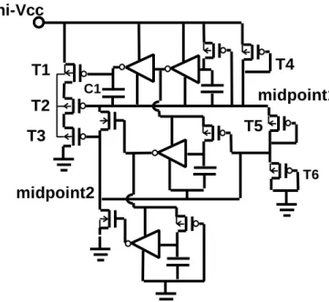
Figure 5 shows the schematic of an improved high voltage PMOS power supply ESD clamp, heretofore unpublished except for a patent filing [11]. Nearly the same circuitry and device dimensions as in Fig. 3 have
been used, but with some important differences. The inverter string for the T1 gate has been increased by one stage (a small inverter, with minimal area impact) so that now the T1 drive circuitry resembles that of Figure 1. It creates a node that is temporarily raised to the full pulsed power supply voltage. This provides maximum gate drive to the transistor T3 during the pulse through the inverter driving T3’s gate. T3 is responsible for grounding the gate of the large PMOS transistor T2 and must sink much capacitively coupled charge. Meanwhile, the T1 gate is pinned to the midpoint by C1 and the inverter driving the gate. After RC timeout (again, 1.5-2 µsec, and easily varied), the inverter driving T3’s gate is powered by a node at the midpoint (nominal process Vcc or less) and all oxide voltages relax to allowed long-term values.
hi-Vcc
T1
C1 T2
T3
T4
T5
midpoint
C2
T6
C3
Figure 5. Voltage-tolerant clamp for Fig. 3 case, having improved circuit design.
gate off at about the same time as its power supply goes to the midpoint.
Figure 6 shows the pulsed I-V result for a v-tolerant clamp designed as in Fig. 5 and having roughly the same size T1 and T2 devices as in Fig. 3. Performance is much improved. At 6V (a good conservative choice for pulsed power supply limit in a submicron process), the Fig. 3 device is between 1 and 1.5 amps, the Fig. 5 device is almost 2 amps and close to the “idealized” curve of Fig. 4. As stated above, stand-alone HBM and CDM ESD tests did not produce any failures, and TLP passed up to 10V on the power supply node, at which point we quit testing because experience has shown that something else will fail at such pulsed voltages on a power supply.
Pulsed I-V
0.0 0.5 1.0 1.5 2.0 2.5
0 2 4 6 8 10
V(Volts)
I (Amps)
Old Vtol Clamp New Vtol Clamp
Figure 6. Pulsed I-V for hi-V PMOS clamp designed as in Fig. 5 (new), and compared to design as in Fig. 3 (old), 0.25 µm process.
Simulated Node Voltages, Fig. 5 Circuit
0.0 1.0 2.0 3.0 4.0 5.0 6.0
4.8 5.2 5.6 6.0 6.4 6.8
Time (ns)
Voltage (V)
hi-Vcc
T1 Gate
T2 Gate
T3 Gate
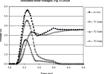
Figure 7. Simulated 2-stack clamp voltages for 80V, 56 ohm TLP pulse, 1 nsec rise time, beginning at the 5 nsec mark. After RC timeout (1-2 µsec) the voltages go to their steady state, off condition.
Further insights into the workings of this design are seen in Figure 7, a circuit simulation of the Fig. 5 circuit in response to a TLP pulse resulting in about
1.35 amps of current (i.e., peak current of a 2kV HBM pulse). Notice how the gates of PMOS FETs T1 and T2 are driven hard to ground in short order, owing to the T3 gate being driven all the way to hi-Vcc. Note that agreement of this simulated I-V data point with Fig. 6 is fairly good. It takes less than an ohm of extra parasitic resistance added to the model to bring it into agreement with Fig. 6, and that is to be expected for the kind of packaged test pattern used for Fig. 6.
II.b. 0.25
µ
m process, 3-stack
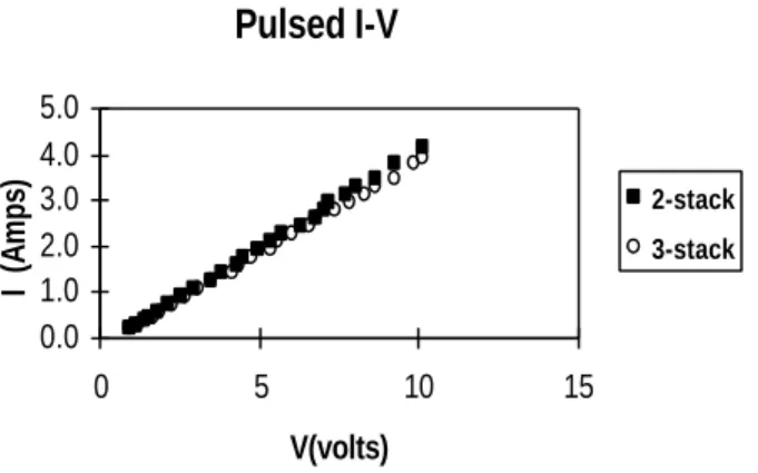
The concepts in Fig. 5 can be generalized to a stack of n large PMOS transistors as a power supply clamp for voltages more than twice the nominal Vcc. Figure 8 shows how (for n=3), the inverters and n-channel devices can be chained together such that all long-term voltages across the thin oxides are legal, yet the pulsed behavior drives the n-channel gates (whose drains in turn ground the T1-T2-T3 gates) as hard as possible. These extra PMOS stages come at the price of more area because the gates are all in series and more gate width must be added to sink the same amount of current. Even so, the layout efficiency in the 0.25 µm process is good, as the area of the 2-stack cell (as in Fig. 5) is only 1.8 times the size of a 1-stack cell (as in Fig. 1), despite the extra drive circuitry and more width (4,000 vs. 3,000 µm) for each of the two gates. A 3-stack clamp as in Fig. 8, tolerating three times the ordinary supply voltage (over 5.5Vdc), has about 1.6 times the area of the 2-stack cell, with 30% more gate width than the 2-stack. The pulsed current drive is similar to that of the 2-stack cell, as shown in Fig. 9.
hi-Vcc
T1
C1
T2
T3
T4
T5
midpoint1
T6
midpoint2
Figure 8. 3-stack PMOS clamp for up to three times nominal Vcc, with chained inverters and NMOS devices to enhance gate drive of T1, T2 and T3
.
Gate lengths of the clamps under discussion in this paper are above the process minimum, ranging from 10-30% above the minimum. The choice of gate length is driven by the desire for current sinking ability, which trades off against subthreshold leakage of the off device. For stacked v-tolerant devices, only the top device in the stack is important for leakage, so to cut down on leakage (particularly at high temperature), only the gate of T1 need be lengthened.
Pulsed I-V
0.0 1.0 2.0 3.0 4.0
0 5 10 15
V(volts)
I (Amps)
2-stack
3-stack
Figure 9. Pulsed I-V of 3-stack vtolclamp compared to 2-stack vtolclamp, 0.25 µm process.
Figure 10 shows measured leakage current vs. temperature for the 2- and 3-stack designs of Figs. 5 and 8 in the 0.25 µm process, at the highest voltages (supply + 10%) for each case. At room temperature
the leakage can always be arranged to be submicroamp, and depends on the length of the bias transistors T4, T5 and (for Fig. 8) T6. This baseline leakage is mostly independent of temperature. The higher temperature leakage comes mainly from subthreshold leakage of T1, but as stated above this can be reduced by lengthening the T1 gate by a little, at only slight cost to pulsed I-V behavior.
Leakage current
0.1 1 10 100
0 50 100 150
T(C)
I (µAmps)
2-stack @ 3.6v
3-stack @ 5.5v
Figure 10. Leakage current vs. temperature at voltage extremes for designs in Figs. 5 and 8.
II.c. 0.18
µ
m process
Pulsed I-V
0.0 1.0 2.0 3.0 4.0 5.0
0 5 10 15
V(volts)
I (A
mps
)
2-stack
3-stack
Figure 11. Pulsed I-V of 3-stack vtolclamp compared to 2-stack vtolclamp, 0.18 µm process.
III. Discussion and Conclusions
High-voltage power supplies in submicron CMOS integrated circuits are needed because of low operating voltages and the need to be compatible with higher-voltage signals that arise when communicating with other chips. These power supply lines can be ESD protected to a high level by using power supply clamps composed of large PMOS FETs with multiple gates. These PMOS FETs can be laid out with minimum or near-minimum dimensions without compromising performance, and allow high ESD performance to be achieved more readily than NMOS FETs. The clamp circuits divide the steady-state supply voltage among several gate oxides, thus avoiding oxide wearout. During the ESD pulse, the circuitry uses the full voltage developed across the clamp to drive PMOS gates as low as possible, toward ground, and thus maximize the current sinking. RC timers, built into the cells, restrict the high-current sinking to the desired 1-2 microseconds. Standby leakage is low, set by the current required to sustain a voltage divider string of long-channel FETs.
We have described a general circuit design method for these high-voltage power supply clamps, allowing n stages and corresponding to standing off n times the ordinary Vcc power supply voltage. The two- and three-stage cases were designed, fabricated, and reported in detail here for two submicron processes, 0.25 µm and 0.18 µm. All examples gave excellent stand-alone ESD results for cells of reasonable size. Pulsed I-V curves for these cells revealed their ability to protect power supply lines from ESD damage by keeping the voltage low during the event.
The PMOS clamp designs discussed here, both single-FET and stacked, were pioneered on 0.6 µm and 0.35 µm processes several years ago. The scaling trend has been most interesting, because the clamp cells get smaller for each new process generation, yet can sink the same amount of ESD current, or more, because of shrinking gate and contact dimensions. Fortunately, ESD events themselves are roughly the same for each generation of integrated circuit products. So far we have not encountered thermal limits to sustaining these large pulsed currents in an ever-shrinking silicon area. The PMOS FET’s ability to conduct current very uniformly under conditions of heavy gate bias is believed to responsible for this favorable condition. Scaling of these PMOS power supply clamp devices into submicron CMOS processes of the future is expected to continue.
Acknowledgments
The authors thank Tina Cantarero for laboratory measurements and manuscript preparation, and thank Andy Hou for managerial support. Also, Gene Worley of Conexant Systems, Inc., provided valuable feedback on the technical content.
References
1. T.J. Maloney and S. Dabral, “Novel Clamp Circuits for IC Power Supply Protection”, 1995 EOS/ESD Symposium Proceedings, pp. 1-12. Revised version published in IEEE Trans. on Components, Packaging, and Manufacturing Technology, Part C, 19, pp. 150-161, July 1996.
2. T.J. Maloney, "Designing Power Supply Clamps for Electrostatic Discharge Protection of Integrated Circuits", Microelectronics Reliability 38, pp. 1691-1703 (1998).
3. K. Seshan, T. J. Maloney, and K. Wu, “The Quality and Reliability of Intel's Quarter Micron Process”, Intel Technology Journal, Q3 1998, available at
http://developer.intel.com/technology/itj/q31998.htm
4. T.J. Maloney and T.M. Eiles, "MOSFET-Based Power Supply Clamps for Electrostatic Discharge Protection of Integrated Circuits", US Patent application, filed 3/25/97.
6. E.R. Worley, et. al., “Sub-micron Chip ESD Protection Schemes Which Avoid Avalanching Junctions”, 1995 EOS/ESD Symposium Proceedings, pp. 13-20.
7. M. Bohr, et. al., “A High Performance 0.25 µm Logic Technology Optimized for 1.8V Operation”, 1996 Proceedings of the IEEE International Electron Devices Meeting, pp. 847-850.
8. T. Maloney and N. Khurana, “Transmission Line Pulsing Techniques for Circuit Modeling of ESD Phenomena”, 1985 EOS/ESD Symposium Proceedings, pp. 49-54.
9. M. Bohr, et. al., “A High Performance 0.35 µm Logic Technology for 3.3V and 2.5V Operation”, 1994 Proceedings of the IEEE International Electron Devices Meeting, pp. 273-276.
10. S. Yang, et. al., “A High Performance 180 nm Generation Logic Technology”, 1998 Proceedings of the IEEE International Electron Devices Meeting, pp. 197-200.

![Figure 2 shows transmission line pulsed (TLP, [8]) I-V curves [2,3] for a pmosclamp protection circuit as in Fig](https://thumb-us.123doks.com/thumbv2/123dok_us/8195353.2172590/3.918.101.453.555.746/figure-shows-transmission-pulsed-curves-pmosclamp-protection-circuit.webp)