Comparison of PI Controller and Fuzzy Controller in Transformer less DC-DC Boost Converter
Archana P.
Assistant Professor, Dept. of EEE, NSS College of Engineering, Palakkad, Kerala, India
ABSTRACT: The output voltage generated by the sources such as photovoltaic arrays, the fuel stacks, the super capacitors or the battery sources are very low, in the range of 12-48 V. Hence it must be boosted to a high voltage. Therefore a novel topology for a boost converter, which can achieve a higher voltage gain, is necessary. The proposed converter is derived from a two-phase interleaved boost converter. The advantages of interleaved boost converter compared to conventional topologies include high voltage gain, high efficiency, low input current ripple and better transient responses. Even though high voltage gain can be obtained, the closed loop control of transformer-less boost converter with PI controller results in reduction of the system responses and causes damage to the components used in the system. So, in order to overcome these drawbacks a quadrupler voltage boost converter with Fuzzy Logic Controller (FLC) is presented. Here simulation models of transformer-less interleaved boost converter with PI controller and Fuzzy Logic Controller in MATLAB was developed. The analytical model for the switching intervals has been validated with the simulation results using MATLAB simulation tool.
Keywords: DC-DC converter, PI Controller, Fuzzy Logic Controller, Quadrupler, Interleaved Boost Converter.
Introduction
The voltage provided by a number of small power generating sources such as renewables is usually low in amplitude. As a result of this, boost-type architecture with a large voltage gain is required to link this voltage to an inverter.A traditional boost converter can achieve an infinite voltage gain as the duty cycle approaches 100% in theory, but in practice, the leakage resistance in the inductor-charging loop limits the boost ratio.Because of this, a boost converter is not used when the required boost ratio is higher than four. Another important requirement is to drain a continuous current with minimum ripple. Therefore, converters combining these two features are expected to find many applications within the renewable-energy context. In the photovoltaic case, the current ripple impacts the power generation since it produces an oscillation around the MPP reducing the energy extracted from the photovoltaic generator. These characteristics make the boost converter a good candidate to interface the photovoltaic systems. Another possibility to reduce the converter’s input current ripple is given by the interleaving structures. The interleaved structure can effectively increase the switching frequency and reduce the input and output ripples as well as the size of the energy storage inductors.
Literature Survey
proposed converter, the conventional switched capacitor technique makes the switch suffer high transient current and large conduction losses. Yang et al. [4] defines a high step-up ratio converter to achieve higher voltage conversion ratio and further reduce voltage stress on the switch and diode. This converter can provide large step-up voltage conversion ratios. But again, the voltage stress of diodes in those converters remains rather high. In this paper, ref. [5,6 and 7] were taken into consideration while analysing the existing converter, whichdescribes about how the fuzzy logic can be applied to the converter and improve the system responses.
Transformer-Less Boost Converter
The main objective of the topology is to obtain high voltage gain and such characteristic can only be achieved when the duty cycle is greater than 0.5 and in CCM. With duty cycle lower than 0.5 or in DCM, there is no enough energy transfer from the inductors to the blocking capacitors, output capacitors, and load side, and consequently it is not possible to get the high voltage gain as that for duty ratio greater than 0.5. In addition, only with duty cycle larger than 0.5, due to the charge balance of the blocking capacitor, the converter can feature the automatic current sharing characteristic that can obviate any extra current-sharing control circuit. On the other hand, when duty cycle is smaller than 0.5, the converter does not possess the automatic current sharing capability any more, and the current-sharing control between each phases should be taken into account in this condition.
Following assumptions are made in order to simplify the circuit analysis of the proposed converter,
1)All components are ideal components.
2)The capacitors are sufficiently large, such that the voltages across them can be considered as constant approximately.
3)The system is under steady state and is operating in CCM and with duty ratio being greater than 0.5 for high step-up voltage purpose.
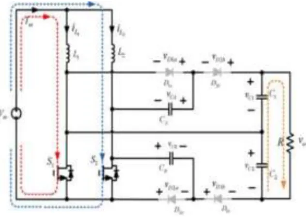
Fig. 1 Transformer-less Boost Converter
Proposed Converter And Operation Principle
One switching period of the converter is divided into five intervals. The detailed theoretical analyses for each mode will be given as follows.
Mode 1: Mode 1 corresponds to the time interval (t0 ≤ t < t1). Before t0, the converter works at a
current free-wheeling stage, and both iL1 and iL2 are equal to zero. For mode 1, switches S1 and S2
are triggered to conduct and diodes D1a, D1b, D2a, and D2b are all OFF. The corresponding equivalent
circuit is shown in Fig.5.3. In this case both iL1 and iL2 are increasing to store energy in L1 and L2,
respectively. The voltages across diodes D1a and D2a are clamped to capacitor voltage VCA and VCB,
respectively, and the voltage across the diodes D1b and D2b are clamped to VC2 minus VCB and VC1
minus VCA, respectively. Also, the load power is supplied from capacitors C1 and C2. The
corresponding state equations are given as follows. Fig. 2 shows the equivalent circuit.
Fig. 2 Equivalent Circuit for Mode 1(t0 ≤ t < t1)
Mode 2: Mode 2 corresponds to the time interval (t1 ≤ t < t2). For this operation mode, switch S1
remains conducting and S2 is turned OFF. Diodes D2a and D2b become conducting. The corresponding
equivalent circuit is shown in Fig.3. It is seen from Fig.3 that part of stored energy in inductor L2 as
well as the stored energy of CA is now released to output capacitor C1 and load. Meanwhile, part of
stored energy in inductor L2 is stored in CB. In this mode, capacitor voltage VC1 is equal to VCB plus
VCA. Thus, iL1 still increases continuously and iL2 decreases linearly.
Fig.3 Equivalent Circuit for Mode 2 (t1 ≤ t <t2 )
Mode 3: Mode 3 corresponds to the time interval (t2 ≤ t < t3). For this mode, operation is same as in
the case of mode1. Both S1 and S2 are turned ON. The corresponding equivalent circuit turns out to
Fig.4 Equivalent Circuit for Mode 4 (t3 ≤ t <t4 )
Mode 4: Mode 4 corresponds to the time interval (t3 ≤ t < t4). For this operation mode, switch S2
remains conducting and S1 is turned OFF. Diodes D1a and D1b become conducting. The corresponding
equivalent circuit is shown in Fig. 4. It is seen from Fig.5.5 that the part of stored energy in inductor L1 as well as the stored energy of CB is now released to output capacitor C2 and load. Meanwhile,
part of stored energy in inductor L1 is stored in CA. In this mode, the output capacitor voltage VC2 is
equal to VCB plus VCA. Thus, iL2 still increases continuously and iL1 decreases linearly.
Steady State Analysis
In order to simplify the circuit performance analysis of the proposed converter in CCM, the same assumptions made in the previous sections will be adopted.
A.Voltage Gain: Referring to Fig. 2 and 3, from the volt-second relationship of inductor L1 (or L2),
the following relations can be obtained.
VinD + (Vin− VCA)(1 − D) = 0 (1)
VinD + (Vin− VCB)(1 − D) = 0
(2)
Also from the equivalent circuits in Fig. 5.4 and 5.5, the voltage VC1 and VC2 can be derived as follows,
VC1 = VCA + VCB =[2/(1 – D)]Vin (3)
VC2 = VCA + VCB =[2/ (1 – D)]Vin (4)
It follows from (3) and (4) that the output voltage can be obtained as follows:
Vo= VC1 + VC2 =[4/(1 – D)]Vin (5)
Thus, the voltage conversion ratio M of the proposed converter can be obtained as follows:
M = Vo/Vin=4/ (1 – D) (6)
B. Voltage Stresses on Semiconductor Components
To simplify the voltage stress analyses of the components of the proposed converter, the voltage ripples on the capacitors are ignored. From Fig. 3 and 4, one can see that the voltage stresses on active power switches S1 and S2 can be obtained directly as shown in the following equation:
VS1,max= VS2,max = [1/ (1 – D) ]Vin (7)
VS1,max= VS2,max = VO/4 (8) From (8), it is clear that the voltage stress of active switches of the proposed converter is equal to one fourth of the output voltage. Hence, the proposed converter enables to adopt lower voltage rating devices to further reduce both switching and conduction losses.
As can be observed from the equivalent circuits in 2 and 4, the open circuit voltage stress of diodes D1a,D2a,D1b, and D2b can be obtained directly as shown in (9).
VD1a,max= VD1b,max = VD2b,max = VO/2 , VD2a,max = VO/4 (9) In fact, it is clear from (8) that the maximum resulting voltage stress of diodes is equal to VO/2. Hence,
the proposed converter enables one to adopt lower voltage rating diodes to further reduce conduction losses.
PI Controller
As the name suggests it is a combination of proportional and an integral controller. In a PI controller the output is directly proportional to the summation of the proportional of the error and integration of the error signal. The PI controller has the ability to reject disturbances and can stabilize the process. The output dc voltage is sensed and compared with a reference output voltage, which gives the error signal. This error signal is then processed by the controller to keep the output voltage constant.
Fuzzy Logic Controller
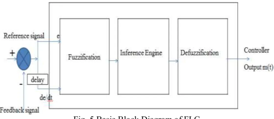
Fuzzy logic is a multivalued logic. It is an approach to computing based on ―degrees of truth‖ rather than the usual―true or false‖ (1 or 0) Boolean logic on which the modern computer is based. The idea of fuzzy logic was first advanced by Dr, LotfiZadeh of the University of California at Berkeley in the 1960s. Fuzzy logic includes 0 and 1 as extreme cases of truth (or ―the state of matters‖ or ―facts‖) but also includes the various states of truth in between.The basic block diagram of fuzzy logic controller is shown in Fig. 5
Fig. 5 Basic Block Diagram of FLC
A.Fuzzy Inference System (FIS) Editor:Fuzzy Logic Toolbox software does not limit the number of inputs. However, the number of inputs may be limited by the available memory of your machine. If the number of inputs is too large, or the number of membership functions is too big, then it may also be difficult to analyze the FIS using the other GUI tools.
B. Membership Function Editor:To define the shapes of all the membership functions associated with each variable C.Rule Editor:To edit the list of rules that defines the behavior of the system
D. Rule Viewer: To view the fuzzy inference diagram. Use this viewer as a diagnostic to see, for example, which rules are active, or how individual membership function shapes influence the results.
E. Surface Viewer:To view the dependency of one of the outputs on any one or two of the inputs— that is, it generates and plots an output surface map for the system.
Simulation Model
The transformer-less boost converter is simulated in the MATLAB-SIMULINK version R2013a. The converter was tested with Vin= 25V DC and Vo= 400V DC. The simulation circuits are shown below.
TABLE I: Component List of Transformer-less Boost Converter with PI Controller
PARAMETERS VALUE
Frequency 40kHz
Inductor L1, L2 253 µH
Blocking Capacitor CA, CB 10 µH
Output Capacitor C1, C2 250 µF
Resistor R 400 Ω
The parameter values of the simulation are given in table I for reference.
Fig. 6 Simulation Model of the Converter PI Controller.
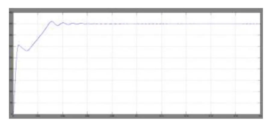
Time (sec) Fig. 7 Output Voltage Waveform of the Converter PI Controller
The switching frequency is chosen to be 40 kHz, both duty ratios of S1 and S2 equal to 0.75. The output
voltage waveform of the converter with PI controller is shown in Fig. 7. The output voltage obtained gives a peak-over shoot of 9.5%. The maximum percent overshoot MP is the maximum peak value of
the response curve, measured from c(∞).
Fig.8 shows the simulation model of the quadrupler voltage converter with FLC. The output voltage is compared with reference voltage which is taken as error. Then again a second time this error is given to a delay to obtain the error changes. Thus the 2 inputs: error and error-change is given to the FLC with rule base as a single input using MUX. Again the output of saturation block is given to delay and added to output of FLC, thus boosting the progress.
Fig. 8 Simulation Model of the Quadrupler Voltage Boost Converter using FLC Then the output is compared with less than or equal to [<=] block and the corresponding pulses are given to gate of two MOSFETs. To ensure 1800 phase shift, one output of saturation block is deducted
Fig. 9 Output Voltage Waveform of Quadrupler Voltage Boost Converter using FLC The output voltage waveform with fuzzy logic converter is given in Fig. 9. The settling time of output voltage waveform is obtained as 0.06sec. The settling time Ts is the time required for the response curve to reach and stay within the 2% of the of the final value.
Time (sec)
Fig. 10 Input Inductor Current of Quadrupler Voltage Boost Converter using FLC
Fig.10 shows the input inductor current for inductors L1 and L2. Both simulated inductor
current ripples are about 2.75A. From the waveform it clear that the proposed converter possesses inherent automatic uniform current sharing capability.
TABLE.II Comparison between PI controller and FLC
Controller used Delay Time(Td) in sec Rise Time(Tr) in sec Settling Time(Ts) in sec Peak Overshoo t( Mp) in
% Transient Behaviour PI Controller 2.84se c 3.95se c
0.1sec 9.5 Oscillatory
Fuzzy Controller 2.19se c 6.45se c
0.06sec 2.7 5
Smooth when
compared to PI
settling time of the quadrupler voltage boost converter with FLC is less compared with that of the PI controller.
Conclusion
Even though it is possible to achieve high voltage gain, the closed loop control of the transformer-less boost converter with PI controller produces a peak overshoot of 9.5% which will damage the system components and reduces the system responses. So, inorder to overcome these drawbacks a quadrupler voltage boost converter with FLC is proposed. The various waveforms of the quadrupler voltage boost converter with uncoupled interleaved inductor topology and FLC have been simulated using MATLAB. Using these results, comparison between transformer-less boost converter with PI controller and the quadrupler boost converter with FLC has been done. By making use of FLC it is possible to reduce the peak overshoot, delay time and the settling time of the converter thereby improving the system response and prevent the damage caused to the components of the system
References
[1] Papanikolaou, N. P., and Tatakis, E. C., ―Active voltage clamp in flyback converters
operating in CCM mode under wide load variation,‖ IEEE Transactions on Industrial Electronics, vol.51, no.3, pp.632–640, 2004.
[2] Li, W., and He,X.,―ZVT interleaved boost converters for high efficiency,
high-step-up DC/DC conversion,‖ IET-Electronics on Power Application, vol.1, no.2, pp.284–290, Mar.2007.
[3] Ismail,E. H.,Al-Saffar,M. A.,Sabzali,A. J., and Fardoun,A. A., ―A family of
single-switch PWM converters with high step-up conversion ratio,‖ IEEE Transactions on Circuits System I, vol.55, no.4, pp.1159–1171, May2008.
[4] Yang,L. S.,Liang,T. J.,and Chen, J. F., ―Transformerless DC–DC converters with
high step-up voltage gain,‖ IEEE Transactions onIndustrial Electronics, vol.56, no.8, pp.3144–3152, Aug.2009.
[5] SameenaNaaz, AfsharAlam and RanjitBiswas, ―Effect of Different Defuzzification
methods in a Fuzzy Based Load Balancing Application‖,
International Journal of Computer Sciences(IJCSI), vol. 8, no. 1, pp. 261-267, Sep. 2011
[6] Rajasekaran, B., and Bharathi,M.L., ―High-Efficiency Modular High Step-Up
Interleaved Dc-Dc Boost Converter Using Fuzzy Controller‖,
International Journal of Scientific & Technology Research(IJSTR), vol. 3, no. 2, pp. 267-271, Feb. 2014
[7] Karthikeyan,R.,Argha Paul and Balamurugan,P., ―Simulation of Interleaved Boost
![Fig. 8 Simulation Model of the Quadrupler Voltage Boost Converter using FLC Then the output is compared with less than or equal to [<=] block and the corresponding pulses are given to gate of two MOSFETs](https://thumb-us.123doks.com/thumbv2/123dok_us/8062420.2135154/7.893.228.661.157.385/simulation-quadrupler-voltage-converter-compared-corresponding-pulses-mosfets.webp)