Metal Oxide Thin Film Growth by Laser Ablation
and Its Applications in High Surface Area
Photoanodes
Rudresh Ghosh
A dissertation submitted to the faculty of the University of North Carolina at Chapel Hill in partial fulfillment of the requirements for the degree of Doctor of Philosophy in the Department of Physics and Astronomy.
Chapel Hill 2012
Approved by:
Charles Evans Rene Lopez
Laurie E McNeil
Thomas J Meyer
c
2012
Abstract
Rudresh Ghosh: Metal Oxide Thin Film Growth by Laser Ablation and Its Applications in High Surface Area Photoanodes
(Under the direction of Rene Lopez)
Thin films are widely used in various applications, including but not limited to
sim-ple reflective coatings for mirrors, electrodes for lithium batteries, conducting substrates
for electronic circuits, gas sensors and solar cells. As the scope of their applications has
widened over the years so has the need to obtain different structural motifs for thin
films. A large variety of fabrication techniques are commonly employed to obtain these
structures. Pulsed laser deposition (PLD) can be used to obtain films varying from
extremely compact and only a few angstroms thick to micron thick porous structures.
In this dissertation I introduce a model for predicting different structures as a function
of laser parameters and deposition environments in a pulsed laser deposition system.
This is followed by a comparison of simulated and experimentally obtained structures. I
then use this model to obtain tailored structures suited for individual applications. One
of the unique structures obtained using the PLD consists of vertically-aligned
struc-tures with nanoparticles as their building blocks. I investigate the superiority of this
unique structure over random nanoparticle networks as photoanodes for titanium
diox-ide (TiO2)-based dye- sensitized solar cells (DSSC). UV-Vis studies show that there
is a 1.4 x enhancement of surface area for PLD-TiO2 photoanodes compared to the
best sol-gel films. PLD-TiO2 incident photon to current efficiency (IPCE) values are
comparable to 3 x thicker sol-gel films and nearly 92% absorbed photon to current
oxide (Ta: TiO2) as photoanode materials. For optimized PLD-Nb2O5-based DSSCs
IPCE values up to 40%, APCE values around 90% and power conversion efficiency of
2.41% were obtained. DSSCs made of PLD-Ta:TiO2 show enhanced photocurrents as
well photo efficiency over those based on PLD-TiO2. I show that this improvement is
due to the slower recombination rates because of the presence of Ta5+. I also show the
applicability of other structures obtained using the PLD. I use very compact thin films
for obtaining the band edges of different potential candidates suitable for photoanodes
of dye sensitized photoelectrochemical cells (DSPEC). This is done by a combination of
x-ray and ultraviolet photoemission spectroscopy (XPS-UPS) and inverse photoemission
spectroscopy (IPS). I also use porous tungsten oxide (WO3) PLD films as H2 sensors.
I determine the optical constants for WO3 in the colored and bleached states and use
them to correlate the gasochromic and electrochromic behavior of WO3. I also introduce
Acknowledgements
I would Like to start of by thanking my advisor, Dr Rene Lopez. His way of letting me do
my own things yet prodding me towards the final destination, helped me in becoming
independent without getting lost in thousands of different directions. He was always
there to offer advise, support and enthusiasm.
I would also like to thank all my committee members for being a part of this effort.
Provided me with many inputs at all times. I am thankful that I had so many extremely
brilliant scientists to show me what being a researcher was all about. Most importantly
for me them gave me confidence and pushed me towards being a better overall scientist.
All the work in this thesis is more a testament of the really intelligent scientists I
have met over the course of my graduate work. I have recieved support and advice
from collaborators within and outside of UNC. I have been trained on experimental
techniques, analysis methods and presentation skills by a bunch of extremely talented
people. I have constantly asked for help and never been said no to.
I would like to thank all the lovely people at CHANL. Every grad student thinks
their research is the most important thing in the world. You guys knew better, yet
played along. Everytime I did something stupid with the instruments you guys made
me feel like it was not really my fault. I have never been without the support of CHANL
and really dont know how research was done here before you guys.
I would also like to thank the people at UNC-EFRC. I would like to thank for all the
diverse research and channeling their efforts towards a common goal.
This would be a good time for me to also thank the unofficial mentors I have had.
Kyle, I really did not know anything at all about dye sensitized solar cells, photophysics,
instrumentation or chemistry. Thank you so much for all the help to not only get me
started , but helping me everytime I needed. Thank you for all the help with the
numerous talks and papers. Ken, as I said to you once, I felt lost everytime people
spoke in the language of chemistry. Thank you for translating that into a language i
understand. Thank you for helping me in projects that you had absolutely no reason
to. Thank you for editing so many things that I wrote, scientific or otherwise. Paul, I
would like to thank you for all the advice with the different projects. You always seemed
to know the right recipes, methods and explanations for physical processes that puzzled
me. Leila, your help with the devices lab is so highly appreciated. Thanks for all the
support in the different projects, even the ones that you and I knew would not work.
I would like to thank not only my lab mates but everyone in the basement of
Chap-man. I have borrowed things from every lab, walked in talking loudly in the middle of
what I later realized were possibly important scientific conversations. We started our
own basement soccer league and that I am prety sure has not happened on any other
floors of Chapman or any other research building.
I would also like to thank the people who have not known me professionally but
have helped me keep my sanity. I would like to thank the lunch group for all the weird
conversations we have had. All the soccer people for allowing me to call you names and
force you into playing soccer even when it made no sense to. I would like to thank so
many of my friends for the rides to and from different places.
I would like to also thank my family (my mom, dad and Urmila masi) for their love
and support. I would like to thank my sister for all the inspiration and tough love. If it
it either.
I would also like to thank my partner, Oana Lungu. Her drive for excellence and
ambition has definitely helped me work harder. Her love for the science she does made
me more passionate about mine.
Table of Contents
Abstract . . . iii
List of Tables . . . xii
List of Figures . . . xiii
List of Abbreviations . . . xvi
1 Introduction . . . 1
1.1 Motivation . . . 1
1.2 Thesis Contributions . . . 2
1.3 Document outline . . . 2
2 Thin film synthesis using pulsed laser deposition: growth model . . 4
2.1 Introduction . . . 4
2.2 Pulsed Laser Deposition: overview . . . 5
2.3 Short time scale description: plasma growth . . . 8
2.4 Particle growth . . . 11
2.6 Model . . . 15
2.7 Film Growth and Characterization . . . 17
2.8 Comparing simulation to experimental results . . . 18
2.8.1 Y-bias to pulse energy . . . 18
2.8.2 Y-bias depletion to background gas pressure . . . 21
2.8.3 Substrate height to target-to-substrate distance . . . 23
2.8.4 Remaining parameters: number of pulses, pulse rate . . . 25
2.9 Conclusions . . . 25
3 Dye Sensitized Solar Cells: Overview of methods, materials and anal-ysis techniques . . . 32
3.1 Introduction . . . 32
3.2 Working principles of a DSSC . . . 34
3.3 Quantitative understanding of effects of different variables . . . 37
3.4 Choice of materials . . . 41
3.4.1 Choice of transparent conductive oxide . . . 42
3.4.2 Choice of photoanode material . . . 42
3.4.3 Choice of chromophore . . . 43
3.4.4 Choice of electrolyte . . . 46
3.4.5 Choice of counter-electrode material . . . 48
3.5 Device fabrication protocol . . . 48
3.5.1 Preparing substrates . . . 48
3.5.3 Preparing counter electrode . . . 49
3.5.4 Preparing dye solution . . . 49
3.5.5 Preparing electrolyte solution . . . 50
3.5.6 Putting it together . . . 50
3.6 Characterization . . . 51
3.6.1 Morphology . . . 51
3.6.2 Chemical and Structural . . . 52
3.6.3 Absorbance . . . 53
3.6.4 Incident Photon to Current Efficiency . . . 54
3.6.5 Current Voltage . . . 56
3.6.6 Electrochemical Impedance Spectroscopy . . . 57
3.6.7 Open Circuit Voltage Decay . . . 57
4 Optimizing Dye Sensitized Solar Cells: different approaches . . . . 63
4.1 Introduction . . . 63
4.2 Directional structures vs random nanoparticle network: Laser ablated TiO2 versus sol gel fabricated TiO2 . . . 64
4.2.1 Experiment . . . 67
4.3 Results and discussions . . . 68
4.3.1 Conclusions . . . 72
4.4 Different growing conditions and morphologies for Nb2O5 using pulsed laser deposition . . . 72
4.4.1 Choice of photoanode material: Nb2O5 . . . 72
4.4.3 Results . . . 75
4.4.4 Conclusion . . . 82
4.5 Comparing undoped TiO2 and Ta doped TiO2 grown under similar con-ditions . . . 84
4.5.1 Choice of material: Tantalum doped TiO2 . . . 84
4.5.2 Film synthesis . . . 84
4.5.3 Characterization . . . 85
4.5.4 Results . . . 86
4.5.5 Discussion . . . 88
5 Other applications of pulsed laser deposited thin films . . . 98
5.1 Introduction . . . 98
5.2 Measurement of energy bands of metal oxides . . . 98
5.2.1 Experimental . . . 99
5.2.2 Results and Discussions . . . 101
5.3 WO3 as gas sensor . . . 105
5.3.1 Experimental . . . 106
5.3.2 Results and Discussions . . . 108
5.3.3 Conclusions . . . 112
List of Tables
2.1 Explanation of variables used in growth model . . . 27
2.2 NanoPLD: operating range of parameters . . . 28
4.1 Nb2O5 device performance: background oxygen pressure variation . . . . 78
4.2 Nb2O5 device performance: gas mix variation . . . 81
4.3 Nb2O5 device performance: thickness variation . . . 83
4.4 Device performance comparison between devices made with undoped TiO2 and Ta-TiO2 electrodes. . . 88
List of Figures
2.1 Schematic diagram of a PLD system . . . 6
2.2 Optics used in our PLD system . . . 7
2.3 Plume growth at different pulse energies . . . 10
2.4 Plume growth at different background gas pressures . . . 11
2.5 Particle formation due to single laser pulse . . . 13
2.6 Particles in ”multiple pulse” mode . . . 14
2.7 Explanation of growth model . . . 16
2.8 Comparison of simulated and experimental structures: y-bias vs pulse energy . . . 19
2.9 Comparison of simulated and experimental structures: y-bias depletion vs background oxygen pressure . . . 22
2.10 Comparison of simulated and experimental structures: y-bias vs pulse energy, spread from seed . . . 23
2.11 Comparison of simulated and experimental structures: substrate height using a patterned substrate . . . 24
3.1 Efficiencies of different solar techniques compared . . . 33
3.2 DSSC structure and energy levels . . . 34
3.3 Step-wise working of a DSSC . . . 35
3.4 IV curve at different conduction band positions of photoanode material . 38 3.5 IV curve for different α values . . . 39
3.7 IV curve at different diffusion coefficients . . . 41
3.8 IV curves for films with different film thicknesses . . . 42
3.9 Chemical structure of common dyes . . . 45
3.10 Action spectra of N719 and N749 . . . 46
3.11 Chemical structures of YD2 and YD2-o-C8 . . . 46
3.12 Steps in device fabrications . . . 51
3.13 Different methods of measuring absorbance . . . 54
3.14 IPCE measurement setup . . . 55
3.15 Transmission line model used for DSSCs . . . 58
4.1 Schematic of random nanoparticle network showing high dye loading . . 65
4.2 Schematic of nanorod based photoanode showing improved charge trans-fer pathways . . . 66
4.3 Schematic for optimized structures for DSSCs . . . 66
4.4 PLD structure compared to sol gel . . . 67
4.5 Electron micrographs of TiO2 deposited at different P(O2) using a PLD . 69 4.6 Photophysical behavior of PLD films deposited at different P(O2) com-pared to sol-gel films . . . 70
4.7 Nb2O5 characterization: XRD and Raman spectra . . . 74
4.8 Nb2O5 sem and tem at different background O2 pressures . . . 76
4.9 Nb2O5 photophysics at different P(O2) . . . 78
4.10 Nb2O5 IPCE increase with Li+ . . . 79
4.11 Nb2O5 structure and photophysics for gas mixes . . . 80
4.13 Nb2O5 thicknesses cross SEM . . . 82
4.14 Nb2O5 thicknesses photophysical characterization . . . 82
4.15 Morphological, structural, elemental characterization of Ta-TiO2 . . . 87
4.16 Photophysical characterization of Ta:TiO2 compared to TiO2 . . . 89
4.17 Photophysical characterization of Ta:TiO2 compared to TiO2 . . . 90
4.18 Comparing TiO2 and Ta:TiO2 fitted transmission line components. . . . 91
5.1 Photoemission and inverse photoemission schematic . . . 99
5.2 TiO2 core levels and valence band . . . 101
5.3 TiO2 core levels and valence band . . . 102
5.4 Nb2O5 core levels and valence band . . . 102
5.5 SrTiO3 core levels and valence band . . . 103
5.6 Metal oxide energy band edges measured using UPS and IPS . . . 104
5.7 WO3 stoichiometry . . . 107
5.8 WO3 change in transmission . . . 108
5.9 WO3 optical constants . . . 109
List of Abbreviations
PLD: Pulsed laser deposition
DSSC: Dye sensitized solar cell
IPCE: Incident photon to current efficiency
APCE: Absorbed photon to current efficiency
DSPEC: Dye sensitized photoelectrochemical cell
XPS: X-ray photoelectron spectroscopy
UPS: Ultra violet photoelectron spectroscopy
IPS: Inverse photo emission spectroscopy
CNT: Carbon nanotube
ICCD: Integrated charge coupled device
SEM: Scanning electron microscope
TEM: Transmission electron microscope
AFM: Atomic force microscope
TCO: Transparent conducting oxide
HOMO: Highest occupied molecular orbital
LUMO: Lowest unoccupied molecular orbital
CB: Conduction band
MLCT: Metal to ligand charge transfer
IMVS: Intensity-modulated-voltage spectroscopy
ITO: Indium tin oxide
FTO: Fluorine doped tin oxide
LHE: Light Harvesting Efficiency
EIS: Electrochemical impedance spectroscopy
Voc: Open circuit voltage
Jsc: Short circuit current density
UHV: Ultra high vacuum
CMA: Cylindrical mirror analyzer
VBM: Valence band maximum
CBN: Conduction band minimum
EA: Electron affinity
PDMS: Polydimethylsiloxane
RBS: Rutherford back scattering
Chapter 1
Introduction
1.1
Motivation
Human ingenuity has produced great technological advances in the last few centuries.
This technological progress has improved our overall quality of life. However, it has
come at the cost of large amounts of energy consumption. If this trend continues,
we can anticipate doubling of the world’s energy needs by 2050 and tripling by 2100.
The increased energy demand has been met over the last couple of decades mostly by
fossil fuels. However, the limited availability of these resources as well as their adverse
environmental effects have forced us to look for other sources of energy.
One of the main alternative avenues being pursued is direct harvesting of the sun’s
energy. In order for the sun to become a viable alternative to fossil fuels we need to
be able to harness this energy cheaply and efficiently. Dye sensitized solar cells (DSSC)
provide hope of such a solar cell. However, for solar energy to become the primary
energy resource we need to improve the efficiency of the devices used to harvest it to
at least close to their theoretical maximum. In order for this to happen we need to
1.2
Thesis Contributions
One of the known bottlenecks for enhanced DSSC performance is the random
nanopar-ticle network that is conventionally used. In this thesis we investigate the effects of
different film morphologies on device behavior. Unlike the conventional sol gel method
we have used pulsed laser deposition (PLD) in order to be able to tailor the film
struc-tures. The high-energy ablation process as well as the decoupling of the evacuation
and deposition steps allows PLD to be used under different reactive and non-reactive
growth environments. This allows us to play with different growth parameters to obtain
tailored structures using this process. Besides just investigating film structures we have
also explored the suitability of other materials with potential to replace TiO2 as the
only DSSC photoanode material.
1.3
Document outline
In order to be able to tailor structures for different applications it is necessary to know
how the film of interest grows by PLD. In the beginning of chapter 2 I briefly talk about
the development in laser systems that helped in the getting to the present state of PLD
systems. This is followed by an overview of the functioning of our PLD system. Next
I discuss about the different occurrences at the different time scales after laser ablation
of the material. I then introduce a model for the film deposition starting from particles
and their interactions as they travel in the target-substrate region. Experimental and
modeled structures are compared as well.
Chapter 3 explains the working principles of DSSCs. I start with a energy level
description of the device components. This is then followed by a discussion of the effect
of different properties of materials used for the devices. Understanding of the working
about the different characterization techniques and the experimental setups I have used.
Chapter 4 focuses on the optimization of photoanodes for DSSCs. In the first
sec-tion I compare PLD-based TiO2 to conventional sol gel-based TiO2 photoanodes. I also
discuss film morphology and its effect on device performance. The next section deals
with photoanodes made of Niobia (Nb2O5). In this section I describe growth conditions
and the resulting structures. This is followed by comparing device performance for
dif-ferent structures for this new material as a photoanode. The third part investigates
TiO2 doped with a metal (Ta). Knowledge from earlier sections is used to synthesize
hierarchical, high-surface-area structures for Ta-doped TiO2 and undoped TiO2.
Pho-tophysical performance of the two types of photoanodes are compared. I discuss what
might be the cause of the differences in performance.
Chapter 5 investigates other possible applications of PLD’s ability to tailor film
struc-tures. I also talk about potential applications for our methods for hybrid-photovoltaics
and DSSC based Tandem cells. Applications to hydrogen gas-sensors are described in
detail.
Chapter 6 summarizes the work done as described in the earlier chapters. It briefly
Chapter 2
Thin film synthesis using pulsed
laser deposition: growth model
2.1
Introduction
Early uses of thin films focused mostly on electronic and optical devices with simple
but high-quality architectures. In these applications it was important to have perfect
surfaces for near-zero-resistance interconnection, and so monolithic films free of particles
were necessary. The inevitable particle formation during PLD severely limited the use
of the technique in the fabrication of such films. This caused a lot of the theoretical and
practical advancements in the field to focus on trying to eliminate particles. Successful
methods to obtain particle-free films included (a) deposition at laser powers below the
threshold energy for particle formation (1), (b) mechanical shutters that use the
differ-ence in time when the atomic plasma and the particles reach the substrate(2; 3), (c) gas
dynamic separation(4; 5), (d) using a molten target(6) among others.
Use of these techniques allowed PLD to be then used for thin film growth for high
temperature superconductors(7; 8), epitaxial oxides on semiconductors(9; 10; 11), and
tribological coatings(12). In more recent years PLD applications have included
car-bon nanotube(CNT)-assisted battery LiCoO2 electrode(13), ZnO nanocones for field
However, as newer thin film applications have arisen, PLD has been embraced for
what was earlier considered its drawback. For example gas sensors(17) and dye sensitized
solar cells (DSSC)(18; 19), need high surface areas and the porous network of particles
produced by laser ablation at high background pressures provides just that. During
work with DSSCs (18; 19) it was observed that different morphological structures could
be formed by deposition under different background pressures. It had already been
suggested that controlling the morphology for such structures using PLD can be done
using the ratio of the target to substrate distance to the plume length(20) as a guideline.
However a growth model for the structure has not yet been proposed.
In order to understand the nanostructure growth mechanism I divide the effect of
each pulse into three separate time regimes. The first is the short time scale that ranges
from nanoseconds to a few hundred microseconds after the ablation (time scale in which
the atomic and molecular species are dominant), the second is the medium time scale
which is in the millisecond range (particle formation due to a single pulse) and continues
till the next pulse hits the target. The longest time scale consists of particle interactions
due to multiple trains of laser shots.
However, before I jump into describing a theoretical model for the nanostructured
growth, it is necessary to give a brief overview of our PLD system.
2.2
Pulsed Laser Deposition: overview
Of the many physical vapor deposition techniques used for thin film growth, pulsed laser
deposition (PLD), with its decoupling of the energy source for vaporizing materials and
the vacuum hardware for the deposition chamber itself provides a unique flexibility in
terms of deposition environments. The directionality of the laser itself in combination
with mobile targets and optics may be used to obtain anything from simple single layered
as an entire deposition laboratory by itself.
Further, in concept a pulsed laser deposition system is possibly the simplest thin
film deposition system. It consists of a high power laser incident on a target that gets
vaporized and is deposited on the substrate. However the actual system is a little more
complex and looks more like figure 2.1.
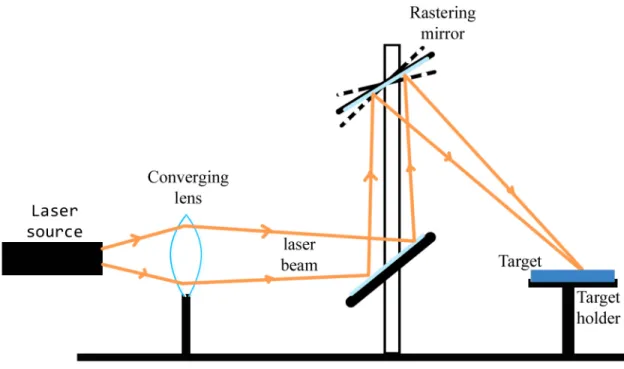
Figure 2.1: Schematic diagram of a PLD system
At the heart of the PLD system is an excimer laser. Our PLD is based on a KrF
laser operating at λ = 248nm. The laser beam is made incident on a small area on
of mirrors. One of these mirrors is motorized to be able to rasterize the beam on the
target.
Figure 2.2: Optics used in our PLD system
In our system there is a moving carousel that can hold up to three targets at the
same time. This is very helpful in obtaining layered structures. The substrate holder is
placed directly over the target being irradiated. The substrate holder is mobile and is
controlled by a motor that can raise the holder up or down. This is important, as I will
show later in the chapter, because the target-substrate distance dictates film structure
and morphology.
The target itself is usually in the form of a small solid disk. Besides the z-motion of
the substrate each of the target holders as well as the substrate holder are capable of
rotating. Together with the rastering of the beam over the target, this assures both a
uniform film deposition over the substrate as well as uniform using up of the target.
physical deposition system lies in the decoupling of the vacuum hardware and the
evap-oration power source. This allows film deposition to occur in different reactive and non
reactive environments, over a large range of pressures as well gas-types. The deposition
occurs inside a chamber that is connected to a vacuum pump. After evacuation the
chamber may be filled with a desired gas to a controlled pressure level. Gas pressure is
monitored by pressure gauges while flow rates are controlled by flow meters.
Besides the variability in deposition environments and target to substrate distance
our PLD system allows us to fabricate films over a larger parameter space that includes
variables such as pulse energy, pulse rate, deposition temperature and the total number
of pulses. The ability to set these parameters and have reproducible films over and over
again is a big advantage compared to sol-gel methods traditionally used to fabricate
porous thin films.
2.3
Short time scale description: plasma growth
In the very short time scale (≤ 200 µs) range the dominant effect is due to the plume
dynamics with respect to the background gas. Wood et al.(21) with great detail came
up with a model for the plume expansion into the background gas dependent on multiple
scattering and hydrodynamical principles considering only on elastic collisions.
Accord-ing to them the plume is made up of plasma that consists of charged ions and neutral
species of the ablated material that act identically as long as the plume growth is
con-cerned. The high ionization energy of the background gas (oxygen in this case) ensures
that the there are no charged species besides those from the target material. Together,
this lends to the argument that the important collisions are those between the plume
and the background gas and the kinetics and scattering processes due to the charged
and neutral species are virtually the same.
in the presence of a background gas into ”fast” and ”slow” components. The ”fast”
component is said to be from mostly the ionic species and is similar to that observed in
vacuum, however the ground state and neutral species are slowed down in the presence
of the background gas.
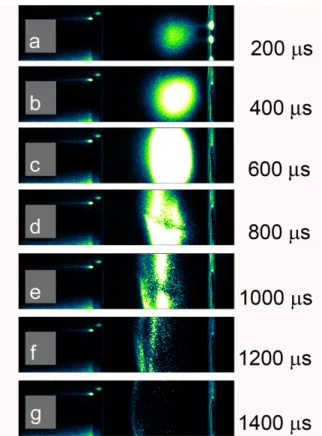
To experimentally observe the changes in plume dynamics, I photographed plume
growth in the presence of background gas as a function of pulse energy, background
gas pressure and target-to-substrate distance were observed. The experimental setup
consisted of a cylindrical lens ( fL=5500 mm) focusing the apertured 248 nm beam from
a Questek 2960 KrF-excimer laser (28 ns FWHM pulse width) to a horizontal line (2.0
cm3 X 0.075 cm) on the face of a TiO2 (99.99%) pellet at an incidence angle of 30o.
Op-tical detection utilized a 1.33 m spectrometer (McPherson 209, 1800 g/mm holographic
grating) outfitted with an intensified, gated diode array (Princeton Instruments
IRY-700RB, 5 ns resolution) and photomultiplier tube (Hamamatsu R955). Fast unfiltered
imaging was performed with a gated, (ICCD), lens-coupled camera system (Princeton
Instruments) with variable gain, 200 to 820 nm response, and variable gating above 5
ns.
Figure 2.3 shows the luminescence from the plume observed for laser pulses with two
different energies (pulse energy = 200 mJ and 300 mJ) in the presence of a background
gas. At higher energies the plume travels faster and reaches a further ”terminal distance”
than the plume from lower energy pulse for the same target material traveling through
the same background gas. At higher pulse energy ejected species from the target have
larger momentum and kinetic energy. These are then expected to need a larger number
of scattering events to be slowed down.
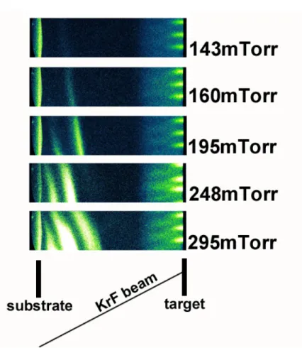
Similar trends are observed with change in background pressure. As shown in figure
2.4, at low pressures ( vacuum and 30mTorr) the plume easily reaches the substrate in
Figure 2.3: ICCD photographs of the visible plasma emissions at different times after KrF laser pulse with different pulse energies is incident on the TiO2 target
the slowing down of the plume causes very little of the plume to be able to reach the
substrate. Further slowing down of the species in the plume causes a larger concentration
of the slow-moving species to continue to exist in the target-substrate distance. This
may in turn lead to formation of particles due to inter-atomic collisions. At higher
background gas pressures there is a larger number of background gas molecules, which
in turn means that species in the plume undergo a larger number of scattering events.
Over a few hundreds of microseconds even for high-energy pulses in low background
pressures the luminescence from the plume dies down. From this time to the time of
the next pulse the slow-moving species that did not reach the substrate collide among
themselves in the target-substrate distance and form particles that become the building
blocks for the nanoparticulate films. Before I talk about the inter-particle and
Figure 2.4: ICCD photographs of the visible plasma emissions in the presence of different background pressures of Oxygen at different times after KrF laser pulse is incident on the TiO2 target
in a laser-ablated system.
2.4
Particle growth
Particulate formation during film growth was one of the main reasons impeding pulsed
laser deposition from becoming more widely used as a thin film growth method. The
combination of research leading to a greater understanding of the particulate growth as
well as newer applications that require nanoparticle-based film structures have renewed
interests in using laser ablation as a deposition method.
In order to understand film structures, it would be a good thing to start with how
particles are affected by different laser parameters. Particles formed by laser ablation
whether it originally started in the solid, liquid or vapor phase. Particles starting either
in the solid or liquid phase are usually much larger, in the sub micron range, compared
to vapor-phase particles which usually range from a few to tens of nanometers in size.
Further, particles formed in the solid or liquid phase are usually irregularly shaped and
do not travel very far from the target in the presence of background gases. The particles
that originated in the vapor phase are only formed in high background gas pressure and
are usually spherical. In our case the high background pressure as well as relatively
large target-to-substrate distance allows us to neglect the particles formed outside the
vapor phase for our simulations (to be presented later).
Particle size, number density and trajectories are dependent on a number of laser
parameters. For a chosen target material and laser wavelength the most important
parameter for variations in particulate characteristics is the laser fluence. The laser
fluence may be controlled by either changes in the laser energy or changes in the laser
spot size. It has been shown that no particles are formed below a threshold energy, and
then the number of particles increases with laser energy until the number levels off(1).
The leveling off at higher energies is due to saturation in the ablation process(23).
Background gas pressure is another laser parameter that needs to be studied in
or-der to unor-derstand particulate formation during laser ablation. The use of background
gases may be characterized as active or passive. Passive use is usually to compensate
for deficiency in certain components. Metal oxides and have been shown to be oxygen
deficient when laser deposition is done in high vacuum compared to when the films are
grown in the presence of background oxygen(17). However the presence of background
gases does much more than just stoichiometric correction as far as particulate growth
is concerned. An increase in the background pressure causes an increased number of
collisions between the vapor phase particles and the background gas molecules. This in
particle-particle collisions because the particles continue in the target-substrate region
for a longer amount of time. Matsunawaet al.(24) have shown that with increased
back-ground pressure there is a larger variation of particle sizes with a shift of the distribution
towards larger particles. They also showed a larger concentration of smaller particles
closer to the substrate which supports the earlier argument.
Figure 2.5: Particle formation and evolution due to a single laser pulse ablating target material.
The particle formation and motion in the target-substrate region is shown in figure
2.5. Initially particles are injected close to the substrate. These high-energy particles
then expand into the cooler region that is occupied by the background gas. As they
expand into this region they suffer collisions with the gas molecules as well as among
themselves, which then slows down the expansion process. Inter-particle collisions are
collisions are smaller and have conserved more of their forward momentum. This causes
the smaller particles to move towards the substrate faster while the larger slow-moving
particles form the tail. This may be the reason for the larger concentration of smaller
particles closer to the substrate (24). Over a long period of time these particles will
reach a terminal distance from the target. This is the distance at which the initial
forward momentum that was imparted to the particles by the laser pulse is completely
lost because of scattering events.
2.5
Multiple Pulse mode
In a PLD system there is a train of pulses time-separated from each other by the
inverse of the pulse rate, each of which introduces new atomic, molecular and particle
species in the target-substrate region. Particles formed from individual pulses continue
to exist in the target-substrate distance over very long periods of times (seconds). This
forces particles from subsequent pulses to interact with those from the previous ones.
The amount of interaction will depend on deposition parameters like pulse energy and
background gas pressure. For higher pulse energies, particles will need larger scattering
events to lose all of their initial energy. This in turn means they travel faster and
reach a greater distance from the target by the time the new species is introduced. This
reduces the interaction between particles from different pulses. The effect of background
pressure is the opposite. Increased background gas pressure translates to a larger number
of collisions, which in turn means a faster slowing down of the particles. This forces
a larger amount of interaction with particles from the subsequent pulses, as shown in
figure 2.6.
2.6
Model
Computer models to study similar structures are common and include the
diffusion-limited aggregation(25) and deposition diffusion aggregation(26). For this model I use a
modified diffusion-limited aggregation approach. Before going on to explain the results
obtained it is necessary to explain the basis of this model, the different parameters that
I have used and what they represent in the physical sense, table 2.1.
For every laser pulse ablating the material a given number of particles <variable
name = injection amount>is injected in the region between the target and the substrate.
These particles move randomly with an initial overall preferred direction<variable name
= y bias>towards the substrate. The number of injected particles as well as the initial
particles undergo this motion they have a probability of colliding with the background
gas molecules (which will depend on the background gas pressure). For every scattering
event there is a loss of forward momentum <variable name = y bias depletion>. Once
these mobile particles reach the substrate they become immobile <particles.mobile =
true⇒particles.mobile = false>to form the first layer. This is not necessarily a uniform
layer but more like seeds on the substrate. The subsequent particles may land on the
bare substrate or on one of these seeds. Mobile particles that collide with immobile
particles may or may not get stuck depending on the amount of energy (dependent on
y bias that still remains in the particle after y bias depletion) that they are incident
with. If they collide with the stuck particle with energy greater than a threshold energy
<variable name = threshold energy> they lose some energy, which depends on the
material cohesiveness<variable name = stickiness>, and bounce back to their previous
position and continue with their random motion. For lower-energy particles, striking a
stuck particle causes them to get stuck <particles.mobile = true ⇒ particles.mobile =
false>. Figure 2.7 depicts this sequence of steps.
2.7
Film Growth and Characterization
In order to compare our model to nanostructured PLD-films, I grew metal oxide films
from the corresponding targets using a KrF excimer laser (248 nm) focused with a 60
degree incidence angle into the chamber and rastered over the target. The resulting
plume was directed towards the substrate held above the target. Both the target and
the substrate were continuously rotated at 40 rpm and 20 rpm, respectively, for uniform
deposition. Prior to deposition, the PLD chamber was evacuated to a base pressure
of 6 x 10 -6 Torr. Variable parameters for the pulsed laser deposition system and the
corresponding operating ranges are noted in table 2.2
microscope (SEM) or transmission electron microscope (TEM). Scanning electron
mi-croscope images are obtained using a Hitachi S-4700 operated at an accelerating voltage
of 2 kV. Cross sectional images from SEM micrographs are obtained by cleaving the
Si substrate and then using a L-mount. Transmission electron microscope images were
obtained in the normal transmission (TEM) mode using JEOL 2010F-FasTEM using
200kV accelerating voltage. In order to obtain single nanostalks to be observed using
TEM, films were scraped off the Si substrate and added to ethanol. These were then
sonicated for 30 minutes and were then put on the TEM grid.
2.8
Comparing simulation to experimental results
2.8.1
Y-bias to pulse energy
To start off I modulate the ”y-bias” parameter. The term ”y-bias” may be considered
as a misnomer as instead of a constant bias during the motion of the particles, this
variable refers to the forward momentum the particles start with. This initial forward
momentum is provided by the pulse energy. Therefore any change seen in the
sim-ulated structures obtained by changing ”y-bias” should be similar to changes seen in
experimental structures due to changes in laser pulse energy.
In these simulations every particle in the region will perform a modified random
walk with a preferential direction. This directionality is provided by the ”y-bias” (or
forward momentum) parameter. Each particle starts of with a given ”y-bias” which will
dictate its subsequent motion. In figure 2.8 I show the effect of modulating ”y-bias”
in this model with all other parameters held constant and the corresponding structures
obtained.
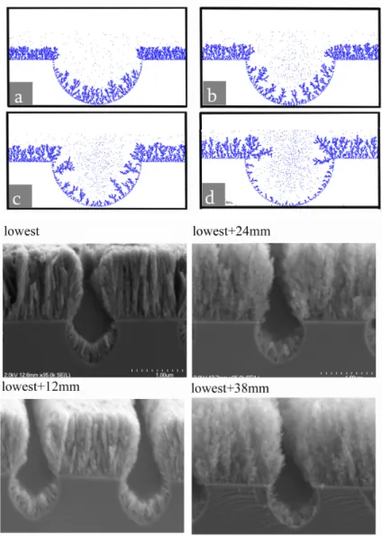
In the simulations which show structure progressions from lowest to highest y-bias,
very compact structure at highest bias (d). At y-bias values in between we see vertically
aligned structures which look like trees. The experimental versions of these structures
are obtained by changing the deposition parameter of pulse energy (shown in the second
panel). The structures do show similar trends of increased porosity as shown in the
simulated figures. There are however certain differences that can be explained in terms
of experimental conditions. The range of pulse energies obtainable for our pulsed laser
deposition system is relatively small (200 mJ to 300 mJ) and therefore does not allow
us to explore the extreme film structures. Secondly from the scale bars it might be
noted that thicker films are obtained at higher pulse energies opposite to that noted
for simulations done at different y-biases. This is due to pulse energy influencing not
only the y-bias but also the number of particles injected into the system from the target.
Larger pulse energies introduces a larger number of particles which in turn causes thicker
films. For the simulations, one of the parameters was changed at a time in order to isolate
trends coming from individual parameters.
Increased pulse energy will cause a larger number of injected particles, which does
not cause the structural geometry to change much besides making the films thicker as
shown in the figure.
To quantify the results from simulations I introduce the terms seed number, average
path length, porosity. In this code every immobile particle is given a path number.
The path number is a measure of how far an immobile particle is from the substrate.
The initial particles that land on the substrate have a path number zero, and are called
seeds. The total number of particles with path number equal to zero is the seed number.
Particles that land on these particles then have a path number 1, which is one higher
than that of the particles they stuck to and this continues. The average path length
from the outermost particles to the substrate is then the average path number. The
film height to the area covered by the immobile particles.
2.8.2
Y-bias depletion to background gas pressure
Once the particle with a given initial ”y-bias” has been injected in the target-substrate
region it will start performing the modified random walk. However, for every step in
the random walk it will lose part of its initial forward momentum because of the ”y-bias
depletion”. In a physical sense this corresponds to what might be expected to occur
in the presence of a background gas. During growth processes in the presence of an
increased background gas pressure, particles will collide more with the gas molecules
and will lose energy faster. This in turn means they will have less of their forward
momentum remaining by the time they reach the substrate if they can get that far.
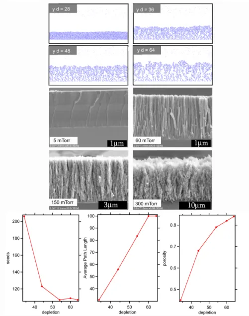
Similar to y-bias changes, the structure can also be modulated using y bias depletion.
Figure 2.9 shows that at the lowest y-bias depletions the films obtained are very compact,
and they become increasingly porous with increase in the value of this parameter with
the possibility of obtaining vertically-aligned structures within a range of its values.
In this case the number of injected particles is not affected by the parameter changed
(background gas pressure). Our system also allows us to vary the range of background
gas pressure from high vacuum to one atmosphere and this allows us to obtain structures
that vary from extremely compact to highly porous as seen in figure 2.9. Further, the
increased porosity also causes film thicknesses to be larger for films deposited at higher
background gas pressures. A larger spreading of the structure from a single seed, as
shown in figure 2.10, is also noted at higher background pressure. Simulations are
Figure 2.10: Comparison of spreading of structures. In the top panel is the simulated structures at different depletion settings (y-bias depletion = d). The spreading is com-pared by measuring the lateral dimension of the simulated structure 20 units away from the seed. In the panel below similar observations are made for structures fabricated at different background gas pressures. Lateral dimensions are measured for the fabricated structures at a distance of 50 nm from the seed.
2.8.3
Substrate height to target-to-substrate distance
Similar trends are also noted for different target-to-substrate distances as shown in figure
2.11. At smaller target-to-substrate distances the particles have more energy left when
they arrive at the substrate due to the lower number of scattering events. This allows
them to form a more compact structure because they do not get stuck to the other
immobile particles immediately. Using a patterned substrate for this part also shows
that the growth is perpendicular to the substrate. This lack of directionality of film
Figure 2.11: Comparison of simulated and experimental structures. Simulated structures are obtained by changing ”substrate height” parameter (lowest at (a) to highest at (d)). Simulations show trends of increased porosity with increased ”substrate height”. In a physical sense ”substrate” corresponds to the target-to-substrate distance. Structures obtained by changing this distance (lowest at (a) to highest at (d)) show similar trends. Further, using a patterned substrate allows us to see if the growth is dependent on the plume direction or the direction of the substrate surface. Growth perpendicular to the circular surface for both experimental and simulated structures confirms that the particles get stuck after the directionality due to the initial energy is lost.
becoming immobile only when they have lost enough forward momentum by means of
2.8.4
Remaining parameters: number of pulses, pulse rate
Other externally-controllable parameters during deposition include the total number of
laser pulses used and the pulse repetition rate. Neither of these parameters has much
effect on the structural geometry. This is due to the fact that they do not control
the directionality or energy with which the particles reach the substrate. Simulated
structures obtained by changing ”number of steps” and ”injection period” confirm these
assumptions.
2.9
Conclusions
Nanostructured films deposited using laser ablation have a unique structure that is due
to the combined effect of plasma, single particles and the continuous collision of particles
as they travel in the target to substrate region. The structures obtained vary from very
compact thin films (grown predominantly by plasma deposition) to very porous thin films
(in the presence of mostly particles). Somewhere in the regime between these extremes
it is possible to get structures that resemble tree-like vertically aligned structures.
Parameters that affect the forward momentum of the particles when they reach the
substrate will also affect the nanostructure of films deposited by pulsed laser deposition.
The final forward momentum of the particles when they reach the substrate will depend
on the initial forward momentum (from pulse energy), the amount of loss in forward
momentum due to scattering (from background gas pressure) and the total number of
scattering events (target to substrate distance). Particles reaching the substrate with low
forward momentum form porous structures while those with larger forward momentum
form compact structures.
This knowledge now allows us to tailor structures from a very compact structure to
vertically-aligned structures. These vertically-vertically-aligned structures are especially useful in
photo-voltaic applications in general and DSSCs in particular as will be theoretically explained
Variable name variable explained
number of parti-cles
number of particles injected into the system initially.
number of steps total number of scattering events being considered. injection period number of scattering events between injections (pulse
rate) injection
amount
number of particles injected for each pulse (same as number of particles)
min radius minimum particle radius max radius maximum particle radius
origin x, y min particles are injected into a random region, close to tar-get and move towards the substrate: minimum of this range in x,y-direction
origin x, y max particles are injected into a random region, close to tar-get and move towards the substrate: maximum of this range in x,y-direction
x step size step size for random walk along x direction y step size step size for random walk along y direction
x bias if any direction is preferred during random walk the bias along x direction can be controlled
y bias the initial forward momentum to the particles. Physi-cally controlled by pulse energy.
x bias depletion for every scattering event there is a probability of colli-sion that causes loss in directionality.
y bias depletion for every scattering event there is a probability of col-lision that causes loss in directionality. In our model this initial directionality is due to pulse energy, which is depleted because of collisions with gas molecules
substrate height target-substrate distance
threshold energy the maximum energy a particle can have for it to be able to collide with a stationary particle and get stuck material
sticki-ness
amount of bias depletion on colliding with a stationary particle.
Parameter start end
Pulse energy (mJ) 200 300
Pulse rate (hZ) 1 100
Background gas pressure (mTorr) 1×10⁻⁵ 1000 Background gas flow (sccm) 1 20 Target substrate distance (mm) 50 88
References
1. Blank, D., IJsselsteijn, R., Out, P., Kuiper, H., Floksura, J., and Rogalla, H. (1992) High Tc thin films prepared by laser ablation: Material distribution and droplet problem. Materials Science and Engineering B(Switzerland) 67–74
2. Barr, W. (1969) The production of low scattering dielectric mirrors using rotating vane particle filtration. Journal of Physics E: Scientific Instruments 2, 1112
3. Dubowski, J. (1986) Epitaxial growth of thin semiconductor films by pulsed laser evaporation, damage and vaporation of CdTe and InSb targets induced with Nd: YAG laser. In Proc. Soc. Photo-Opt. Instrum. Eng., volume 668, 97
4. Gaponov, S., Gudkov, A., Luskin, B., Luchin, V., and Salashchenko, N. (1981) Formation of semiconductor films from a laser erosion plasma scattered by a heated screen. Soviet Physics-Technical Physics 26, 598–600
5. Kennedy, R. (1992) A new laser ablation geometry for the production of smooth thin single-layer YBa2Cu3O7-x and multilayer YBa2Cu3O7-x/PrBa2Cu3O7-x films. Thin Solid Films 214, 223–228
6. Cheung, J. and Sankur, H. (1988) Growth of thin films by laser-induced evapora-tion. Critical Reviews in Solid State and Material Sciences 15, 63–109
7. Dijkkamp, D., Venkatesan, T., Wu, X., Shaheen, S., Jisrawi, N., Min-Lee, Y., McLean, W., and Croft, M. (1987) Preparation of Y-Ba-Cu oxide supercon-ductor thin films using pulsed laser evaporation from high Tc bulk material. Applied Physics Letters 51, 619–621
8. Wu, X., Dijkkamp, D., Ogale, S., Inam, A., Chase, E., Miceli, P., Chang, C., Tarascon, J., and Venkatesan, T. (1987) Epitaxial ordering of oxide supercon-ductor thin films on (100) SrTiO3 prepared by pulsed laser evaporation. Applied physics letters 51, 861–863
10. Fork, D., Fenner, D., Barton, R., Phillips, J., Connell, G., Boyce, J., and Geballe, T. (1990) High critical currents in strained epitaxial YBa2Cu3O7-δ on si. Applied Physics Letters 57, 1161–1163
11. Fork, D., Ponce, F., Tramontana, J., and Geballe, T. (1991) Epitaxial MgO on Si (001) for Y-Ba-Cu-O thin-film growth by pulsed laser deposition. Applied physics letters 58, 2294–2296
12. Auciello, O., Barnes, T., Chevacharoenkul, S., Schreiner, A., and McGuire, G. (1989) Laser ablation deposition of titanium nitride films on silicon substrates at room temperature. Thin Solid Films 181, 65–73
13. Lo, A., Sun, C., Tseng, W., and Kuo, C. (2009) Process and properties of the carbon nanotube assisted LiCoO thin-film battery electrode by pulsed laser deposition. Journal of Vacuum Science & Technology B: Microelectronics and Nanometer Structures 27, 3067
14. Bae, J., Hong, J., Han, W., Choi, Y., and Snyder, R. (2009) Superior field emission properties of ZnO nanocones synthesized by pulsed laser deposition. Chemical physics letters 475, 260–263
15. Zhang, H., Feng, P., Makarov, V., Weiner, B., and Morell, G. (2009) Synthesis of nanostructured SiC using the pulsed laser deposition technique. Materials Research Bulletin 44, 184–188
16. Ray, E., Hampton, M., and Lopez, R. (2009) Simple demonstration of visible evanescent-wave enhancement with far-field detection. Optics letters 34, 2048– 2050
17. Ghosh, R., Baker, M., and Lopez, R. (2010) Optical properties and aging of gasochromic WO3. Thin Solid Films 518, 2247–2249
18. Sauvage, F., Di Fonzo, F., Li Bassi, A., Casari, C., Russo, V., Divitini, G., Ducati, C., Bottani, C., Comte, P., and Graetzel, M. (2010) Hierarchical TiO2 photoanode for dye-sensitized solar cells. Nano letters
20. Bailini, A., Di Fonzo, F., Fusi, M., Casari, C., Bassi, A., Russo, V., Baserga, A., and Bottani, C. (2007) Pulsed laser deposition of tungsten and tungsten oxide thin films with tailored structure at the nano-and mesoscale. Applied surface science 253, 8130–8135
21. Wood, R., Chen, K., Leboeuf, J., Puretzky, A., and Geohegan, D. (1997) Dynam-ics of plume propagation and splitting during pulsed-laser ablation. Physical review letters 79, 1571–1574
22. Leboeuf, J., Chen, K., Donato, J., Geohegan, D., Liu, C., Puretzky, A., and Wood, R. (1996) Modeling of dynamical processes in laser ablation. Applied surface science 96, 14–23
23. Smith, G., Chen, L., and Chuang, M. (1992) Effects of processing parameters on KrF excimer laser ablation deposited ZrO films. In Materials Research Society Symposium Proceedings, volume 235, 843–848
24. Matsunawa, A., Katayama, S., Susuki, A., and Ariyasu, T. (1986) Laser produc-tion of metallic ultra-fine particles. Trans. JWRI 15, 233–244
25. Witten Jr, T. and Sander, L. (1981) Diffusion-limited aggregation, a kinetic crit-ical phenomenon. Physcrit-ical Review Letters 47, 1400–1403
Chapter 3
Dye Sensitized Solar Cells:
Overview of methods, materials and
analysis techniques
3.1
Introduction
One of the grand challenges for the human race is to be able to keep up with the
constantly growing energy needs of our species, while at the same time ensuring that
we protect our environment. In order to be to able to achieve this goal there is an
immediate need for us to shift from our dependence on fossil fuel. The obvious choice is
to move to an energy source that is inexhaustible and clean at the same time. The Sun
with its proven track record of providing enough energy to run all natural processes on
our planet throughout its existence is an excellent candidate. However, in order to tap
into this source we need to find a way to harness this energy. Although there already
exists techniques and products to do this, there still exists certain difficulties that have
stood in the way of solar energy overtaking or even making a significant dent in this
fossil fuel driven world.
Current techniques to tap the Sun’s inexhaustible energy source to produce electricity
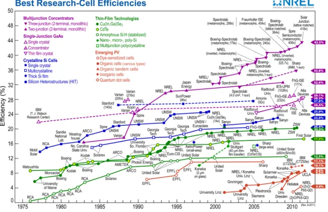
Figure 3.1: Efficiency of different solar techniques and their evolution over the years.
obvious from figure 3.1 the battle for efficiency is being won by multijunction
concentra-tors followed by c-Si and thin film based techniques. However, in order for solar energy
to be able to become competitive overall, efficiency is not the only parameter that needs
to be optimized. The biggest hurdles in the path of the above-mentioned techniques
in replacing fossil fuels remain the high costs and highly energy-consumptive methods
of preparation. Additionally certain widely-used materials for these techniques are not
only toxic (e.g. CdTe) but are also not overly abundant.
On the other hand although emerging photovoltaics do not boast the high efficiencies
of the other techniques, they do provide the advantages of being inexpensive, easy to
fabricate and being made of materials that are relatively abundant. Of the various
devices that are included in this field, the highest efficiencies have been recorded for dye
Although the idea of sensitizing photoelectrodes itself is not new, (1) being able
to use it as a viable solar cell was only demonstrated in 1991 by Brian O’Regan and
Michael Gr¨atzel(2). Since then there has been a great amount of research in the field
which has seen an improvement of over all power conversion efficiency increase from 7%
to its current value of around 13% (3).
3.2
Working principles of a DSSC
Despite the great amount of research in optimizing different parameters, the extremely
simple architecture of DSSCs has remained pretty much unchanged since 1991. A DSSC
consists of the following components: (a) a glass substrate for support, (b) a transparent
conducting oxide (TCO) on the substrate, (c) a semiconductor film, (d) sensitizer dye
adsorbed on the semiconductor film, (e) an electrolyte with a redox mediator, and (f)
a counter electrode that can regenerate the redox mediator. The layout of the different
components in a typical DSSC is shown in figure 3.2 (a). Figure 3.2 (b) shows the
different energy levels that dictate the photophysical behaviour of the cell.
Figure 3.2: (a) Schematic diagram showing different parts of a DSSC, (b) Energy levels for the different parts of s DSSC
sorbed by the dye, it excites an electron from its highest occupied molecular orbital
(HOMO) level to its lowest unoccupied molecular orbital (LUMO) level, thus oxidizing
the dye. This is quickly followed by the injection of the excited electron into the
con-duction band (CB) of the semiconductor. The dye itself is brought back to its normal
state by gaining an electron from the redox electrolyte. The injected electron is
trans-ported through the semiconductor to the TCO by doing an amount of work equal to the
energy difference between the CB of the semiconductor and the redox potential of the
electrolyte.
In principle the functioning of a DSSC maybe divided into eight distinct processes
(4) shown in figure 3.3.
1. Photon absorption and excitation: Light is absorbed by the dye. This is dictated
by the absorption window, the light intensity in that window and the absorption
coefficient (α) of the dye. The absorbed energy from this light excites electrons
from the HOMO level to the LUMO level of the dye. figure 3.3 (a)
2. Radiative recombination: Direct relaxation of the dye back to its ground state in
which the excited electron loses its energy by some radiative process and goes back
to the HOMO from the LUMO level. figure 3.2 (d) This usually has a time scale
in the nanosecond regime. Rate constant = k2
3. Exciton diffusion: The excited electrons may then jump from the LUMO level of
one dye molecule to another. figure 3.2 (e). This may be reduced by ensuring only
uniform monolayer coverage.
4. Interfacial charge transfer: Excited electrons from the dye-LUMO are injected into
the semiconductor-CB. figure 3.2 (f). For an efficient DSSC this should happen in
a picosecond time scale. Rate constant = k4
5. Electron back transfer: Excited electrons from the semiconductor-CB may be
captured by the oxidized species of the electrolyte. figure 3.2 (g). Rate constant
= k5
6. Interfacial charge recombination: Excited electrons from semiconductor-CB may
get captured by the oxidized dye molecules. figure 3.2 (h). Rate constant = k6
7. Electron transport: The excited electrons travel through the network of
may also be lost to the lower-energy states of the semiconductor by non-radiative
processes like phonon relaxation.
8. Electrolyte to dye electron transfer: Electrons from the electrolyte constantly
re-plenish the dye-HOMO level, figure 3.2 (j).
The main driving force for the efficient working of a DSSC is the very fast interfacial
charge transfer. When the electron is in the dye-LUMO, of the two processes that are
possible, (2) and (4) from above, the rate constants (k4/k2 ∼ 1000) overwhelmingly
favors charge injection. Once they have been injected into the semiconductor CB, rate
constants (k5/k6 ∼ 100) favor electrons being lost to the electrolyte over being lost to
the dye. In light of these rate constants the steps (2) and (6) may be ignored for most
optimized systems(4).
3.3
Quantitative understanding of effects of
differ-ent variables
In order to have a very basic understanding of the effects of the different parameters
on the functioning of a dye sensitized solar cell we use a mathematical model based
on the work of Wurfel(5). The code used for the simulation can be downloaded from
www.physics.unc.edu\∼rudresh\dssccode.nb.
The first parameter we vary is the position of the conduction band (Ecb) of the
photoanode. Since I-/ I3- is the redox couple predominantly used for these systems we
keep that constant. In keeping with this convention we fix the I-/ I3- redox level at
-4.95 eV. Ecb is varied from -4.0 eV to -4.9 eV. From the I-V curves obtained (shown in
figure) it can be noted that the only effect the change in Ecbhas is that of changing the
Voc. This is understandable because the change in Ecb changes only the position of the
been injected to this Ecb the transfer and collection of those electrons is independent of
this energy level.
Figure 3.4: IV curves for different positions of conduction band edge, Ecb, of materials used as photoanaodes.
Once we know that electrons can be injected into Ecb, we can think of the other
possibilities. The next step is to know how electron concentration in the Ecb affects
device behavior. The electron concentration in Ecbwill depend on the injection efficiency
of the molecules and the total number of electrons in the LUMO of the dye. This will
in turn depend on the absorption coefficient of the dye and the light intensity. For our
simulations we consider only one light intensity and unity light efficiency (similar to
what is expected for TiO2 based dye sensitized solar cells). We consider all the other
steps using a single parameterα in our simulations.
From the IV curves we see that unlike the changes caused by changes in Ecb, changes
Figure 3.5: IV curves for different values of α.
of the photoanode. This increase in electron concentration pulls the Fermi level upward
and therefore is observed as an increased Voc. The increased conduction band electrons
are also observed as a larger photocurrent.
The trends of Voc and Isc shown in the graphs also reiterate this. Initially with an
increase inαthere is a large change in the position of the quasi-Fermi level (and therefore
the Voc) but as the quasi Fermi level gets closer and closer to the position of Ecb, the
value of Voc saturates off. A similar trend, though slower, is seen for Isc. Initially with
an increase in α there is a larger increase in the number of photo-generated electrons.
However once the system has absorbed all the light there is no further increase in the
number of photo-generated electrons.
The electrons in the conduction band may either recombine with the electrolyte
with a rate constant Krcb or diffuse through the photoanode with a diffusion coefficient
Dcb. The IV curves due to changes in Krcb are shown in the figure. Like changes in α,
electrons can go through the photoanode and reach the conductive substrate. Lowering
Krcb further does not cause any increase in Isc. However the lower Krcb in this regime
causes the electrons to populate the conduction band for longer, causing a positive shift
in Ecb and therefore a higher Voc.
At higher Krcb electrons are lost faster and not all the photo-generated electrons can
reach the conductive substrate. This is observed as a lower Isc. In order for improved
device performance Krcb needs to be reduced.
Figure 3.6: IV curves for different recombination rates, Krcb, for materials used as photo anodes.
The diffusion coefficient Dcbdoes not cause any changes in Voc. However it does cause
a rapid drop in Isc at corresponding diffusion lengths smaller than the film thickness.
At diffusion length values comparable to and larger than the film thickness all electrons
can pass through and therefore no further changes in photocurrent are observed.
Change in film thicknesses has two possible effects. Increase in thickness causes a
Figure 3.7: IV curve as diffusion coefficients, Dcb, is varied
larger number of photo-generated electrons. However with a very thick film there is also
a larger amount of electrons lost due to recombination. This shows up as a saturation
in the photocurrent at a given film thickness with no gains by making it any thicker.
For an optimized device, a high Vocand high Iscare desired. This may be obtained for
a photoanode with high conduction band (lower than the LUMO of the dye), high light
absorption (controlled by the absorption coefficient of the dye as well as the amount of
dye loading), low recombination rate, high diffusion constant, a thickness optimized for
efficient light absorption and an overall device architecture that lowers resistive losses.
In the next section I describe how these choices are made.
3.4
Choice of materials
In the last section I discussed the rationale for choosing certain properties for an efficient
Figure 3.8: IV curves as film thicknesses, d, is changed.
improvements are possible.
3.4.1
Choice of transparent conductive oxide
Conductive substrates are required for charge transfer out of the cell. The usual
trans-parent conducting oxides are indium doped tin oxide or fluorine doped tin oxide.
3.4.2
Choice of photoanode material
The major breakthrough in using dye sensitized films for solar cells came in 1991 with
the use of a mesoporous network of TiO2 as the photoanode. Since then a variety of
other materials, including other binary metal oxides (ZnO(6),(7), Nb2O5(8),(9)), ternary
oxides (SrTiO3(9),(10)), doped metal oxides (Ta(11) or Nb(12) doped TiO2) or core shell
structures (ZnO coated SnO(13)) have also been tried. In recent years work has focussed
on not only the proper choice of material but also the optimization of the morphology
nanotubes(14) and single crystal nanorods(15).
In spite of the works on other materials and structures, TiO2 nanoparticle-based
films still dominate the DSSC device landscape. Although different crystalline forms
(rutile, brookite, anatase) of TiO2 exist naturally, the larger band gap and higher Ecb
of the anatase phase makes it the favorite for DSSC applications. The usual fabrication
processes of TiO2 films are based on sol-gel or hydrothermal routes starting from
hy-drolysis of a titanium precursor such as titanium(IV) alkoxide using water as a catalyst
in an acid or base, followed by hydrothermal growth and crystallization. Control of
the shape, size and properties may be accomplished by tuning the rate of hydrolysis,
temperature, and water content.
Although much work has been done in growing TiO2 films this way, the advances of
this method cannot be readily translated when trying to develop other materials. A lack
of clear understanding of the growth processes prevents the tailoring of morphologies of
films. Together, these factors make controlled investigations of different materials and
different structures for DSSCs a difficult process.
3.4.3
Choice of chromophore
The first step in the conversion of light to current in DSSCs involves the absorption
of light by the chromophore. The absorption of light by the dye starts off a series of
reactions (shown below) that act as the functioning steps of a DSSC.
dye + hν → dye∗
dye∗ → dye+ + e-(injected)
dye+ + 3/2I- → dye + 1/2I
3-I3- + 2e- → 3I
-In order for a DSSC to be highly efficient it must start with a dye that satisfies