! ! ! ! ! DESIGN!OF!A!NANOSCALE!TIME/OF/FLIGHT!SENSOR!AND!AN!INTEGRATED! MULTISCALE!MODULE!FOR!THE!POINT/OF/CARE!DIAGNOSIS!OF!STROKE! ! ! ! ! ! Matthew!Andrus! ! ! ! ! ! A!thesis!submitted!to!the!faculty!at!the!University!of!North!Carolina!at!Chapel!Hill!in! partial!fulfillment!of!the!requirements!for!the!degree!of!Master!of!Science!in!the! Department!of!Biomedical!Engineering.! ! ! ! ! ! Chapel!Hill! 2015! ! ! ! ! ! ! ! ! ! ! ! ! ! !!!!! !!!!!!!!!!Approved!By:! !
! ! ! ! ! ! ! ! ! !!!!!!!!!!Steven!A.!Soper!
!
! ! ! ! ! ! ! ! ! !!!!!!!!!!Frances!Ligler!
!
! ! ! ! ! ! ! ! ! !!!!!!!!!!Glenn!Walker!
!
ABSTRACT"
Matthew"Andrus:"Design"of"a"Nanoscale"Time=of=Flight"Sensor"and"an"Integrated" Multiscale"Module"for"the"Point=of=Care"Diagnosis"of"Stroke""
(Under"the"direction"of"Steven"A."Soper)" "
" Stroke"is"a"leading"cause"of"death"and"disability"in"the"United"States,"however," there"remains"no"rapid"diagnostic"test"for"differentiating"between"ischemic"and" hemorrhagic"stroke"within"the"three=hour"treatment"window.""Here"we"describe"the" design"of"a"multiscale"microfluidic"module"with"an"embedded"time=of=flight"nanosensor" for"the"clinical"diagnosis"of"stroke.""The"nanosensor"described"utilizes"two"synthetic" pores"in"series,"relying"on"resistive"pulse"sensing"(RPS)"to"measure"the"passage"of" molecules"through"the"time=of=flight"tube.""Once"the"nanosensor"design"was"completed," a"multiscale"module"to"process"patient"samples"and"house"the"sensors"was"designed"in" a"similar"iterative"process.""This"design"utilized"pillar"arrays,"called""pixels""to"
TABLE"OF"CONTENTS" "
LIST"OF"FIGURES"AND"TABLES...vi" CHAPTER"1:"INTRODUCTION...1" 1.1"Diagnosis"with"LabAOnAAAChip:"Stroke...1" 1.2"SingleAMolecule"Detection...3" 1.3"Coulter"Counter"and"Resistive"Pulse"Sensing...6" 1.4"Thermoplastics"in"Microfluidic"Applications...7" 1.5"A"Universal"Molecular"Processing"System"(uMPS)...10" 1.6"Structure"of"the"Thesis...12" CHAPTER"2:"A"NANOSALE"TIMEAOFAFLIGHT"SENSOR...14" " 2.1"Sensor"Description"and"Design"Constraints...14" " 2.2"Resistive"Pulse"Sensing"(RPS)...18" " 2.3"COMSOL"Assisted"Iterative"Design...19" " 2.4"Fabrication"of"a"Nano"TimeAofAFlight"Sensor...34" CHAPTER"3:"INTERGRATED"MULTISCALE"MODULE"FOR""
LIST#OF#FIGURES#AND#TABLES#
#
Figure#1.1#–#Example#optical#train...5#
Figure#1.2#–#Coulter#counter#patent#drawing...6#
Figure#2.1#–#CAD#drawing#of#nanosensor#geometry...14#
Figure#2.2#–#Imported#flightMtube#geometry#and#electric#field#trace#from#COMSOL...22#
Figure#2.3#–#Initial#3D#model#with#field#strength#shading...23#
Figure#2.4#–#Input#funnel#length#experiment#results...26#
Table#2.1#–#Results#from#the#TBE#buffer#models...27#
Figure#2.5#–#Results#from#the#particle#size#simulation...29#
Figure#2.6#–#Model#for#nanopore#length#simulations...30#
Figure#2.7#–#COMSOL#results#from#the#pore#length#experiments...31#
Figure#2.8#–#Blockage#current#traces#for#20,#50,#and#80#nm#pores...33#
Figure#2.9#–#SEM#image#for#nanochannel#milled#into#silicon#with#FIB...35#
Figure#2.10#–#3D#AFM#image#of#the#50#nm#nanopore#within#the#nanochannel...37#
Figure#3.1#–#Overview#of#the#final#chip#design...40#
Figure#3.2#–#Steady#state#hydrodynamic#flow#profile#through#chip...41#
Figure#3.3#–#Hydrodynamic#flow#profile#at#critical#regions...42#
Figure#3.4#–#Particle#trace#illustrating#even#distribution#through#chip...43#
Figure#3.5#–#Proportional#arrow#plot#for#electric#field#strength#in#chip#...44#
Figure#3.6–#Electric#field#arrows#at#critical#regions#on#chip...45#
Figure#3.10#–#Close#up#images#of#final#device#with#features#labeled...49#
#
CHAPTER 1
Introduction
1.1Diagnosis with Lab-On-A-Chip: Stroke
Lab-on-a-chip (LOC) technologies can allow new diagnostic devices to reach
patients in both the developed and the developing world in novel and powerful
ways.1 These devices can allow for highly sensitive, specific, and reproducible point
of care tests with little more input needed from the user than the insertion of a
patient sample. LOC devices possess a number of inherent advantages over
traditional laboratory tests, including portability, low solution volumes, efficiency,
and potentially cost.1 These advantages make these devices especially well-suited
for mobile applications such as emergency services vehicles.
Herein is described work towards a device for the rapid diagnosis of stroke
in the pre-hospital setting. Technologies such as those that we are developing can be
used in identifying and tracking genetic biomarkers that were previously too rare to
detect and accurately measure over time with the existing diagnostic technologies.
To generalize, this technology will allow for rapid and portable diagnoses utilizing
very rare biomarkers.
A few facts and statistics will elucidate the importance of a new diagnostic
there are two variations of a stroke, ischemic and hemorrhagic, which are
indistinguishable by current diagnostic methods such as computed tomography
(CT) or magnetic resonance imaging (MRI). It is critical that the distinction made
between these two disease states as quickly as possible because the treatments for
ischemic and hemorrhagic stroke are very different and can actually be fatal if
administered to a patient who has suffered the other type. The biggest example of
this in assessing whether or not to administer tissue plasminogen activator (tPA), a
treatment that is known to be very effective in ischemic stroke, yet is very
dangerous and often fatal in hemorrhagic stroke. A rapid diagnosis could allow
physicians to make the proper decision early in the treatment process. Additionally,
there is only about a four hour treatment window available to stroke patients,
lending to the common phrase “time is brain”.3,4 Rapid diagnostics will be critical to
allow physicians to make the necessary diagnostic decisions within this pressing
time window. Unfortunately, no reliable biomarkers have yet been discovered in
the peripheral blood for indicating what type of stroke the patient has suffered.
However, it has been demonstrated that mRNA can be harvested from specific white
blood cells and a panel gene expressions can be utilized as a reliable biomarker for
the diagnosis of stroke.5,6 Our system could allow for these mRNA panels to be
quickly assessed in patient blood samples in a point-of-care setting. In a disease like
stroke where getting the diagnosis correct very rapidly can save lives, this type of
1.2 Single-Molecule Detection
The goal of single-molecule detection (SMD) is to probe individual molecules
in solution, gaining as much information about the molecule as possible. In addition,
SMD can be used as a detection foundation in the clinic to detect very rare
biomarkers and provide quantitative information with exquisite sensitivity due to
the digital nature of the readout. The first detection of a single molecule occurred in
1989 by W.E. Moerner, who imaged a single pentacene molecule inside a solid
crystal utilizing an absorbance measurement.7 A year later at Los Alamos National
Laboratory, Shera et al. demonstrated the detection of single fluorescent molecules
in solution.8 This successful experiment sparked a new area of research and many
groups began working on and improving upon this technology for the accurate
detection of single molecules in solution. Trautman et al. successfully imaged a
single fluorophore on an air-dried surface in 1994 and Funatsu et al. imaged a single
fluorophore attached to a protein molecule using total internal reflection
fluorescence (TIRF) microscopy in 1995.9,10 This optical detection of a single
molecule in fluid marked the birth of single molecule detection technologies. These
technologies opened a new era in life sciences technologies, especially in the area of
diagnostics. Biomolecules are now able to be individually probed, pulling important
data out of previously averaged ensemble measurements.11 This allows for the
detection of much more scarce and specific biomarkers for diseases that would
otherwise be extremely difficult to diagnose with traditional bulk measurements. In
exquisite analytical sensitivity compared to analog measurements, which consist of
bulk measurements.
Microfluidic systems have become a very popular platform for single
molecule studies due to the ability physically isolate particles and utilize extremely
low concentrations and low solvent volumes.12,13 Nanofluidics are even more
attractive for SMD studies, as the benefits of microfluidics are further increased as
the device dimensions continue to decrease. Moerner et al. has demonstrated that
single molecules can be so confined in these nano-structures that Brownian motion
is markedly decreased, allowing for more accurate observations.14
Traditionally, SMD schemes have relied on fluorescently tagging molecules to
make them ”visible” at specific wavelengths. This is an excellent strategy that allows
for multiple channels to be monitored separately and simultaneously by utilizing
multiple markers and excitation sources.15 Unfortunately, these types of systems
require sophisticated and fragile optical trains that require precise alignment and
calibration. While this type of system thrives in the lab, it can become useless once
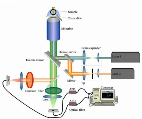
taken out into the field for point-of-care diagnostics. Figure 1.1 shows an example
optical system utilized by our lab group; many of the components are made of glass
and the alignments required for accurate measurements are on the scale of
Figure 1.1 Example optical train for a SMD system. With many fragile components,
including 532 nm and 650 nm lasers, and precise alignment required for accurate measurements; this type of system is not adapted to portable, rugged applications. (Designed by Zhiyong Peng)
Electronic detection modalities not only overcome this portability limitation,
allowing SMD systems to be utilized in situations that would otherwise be
unworkable, but also have advantages in both cost and miniaturization, making
them much more scalable and commercially viable.16,17 Often, these electronic
detection schemes involve nanowires or nanogap electrodes patterned into the
fluidic substrate.18–21 However, there are challenges with the fabrication of
electronic systems that can achieve single-molecule detection. Firstly, creating
durable electrodes at the sizes required for a good signal to noise ratio is very
electrode strategies may work well in glass microfluidics, thermoplastic chips
require different solutions for electrical detection of single molecules to be feasible.
1.3 Coulter Counter and Resistive Pulse Sensing
In 1949, Wallace H. Coulter patented his method for counting particles
suspended in a fluid.22 This approach involved passing particles through an orifice
with a current applied across the fluid. As the particle passes through the orifice,
taking up volume, and displacing ions, the change in resistance across the device can
be measured. The principle can be understood from one of Coulter’s original patent
drawings seen in Figure 1.2. Coulter originally created his technology for the US
Navy during World War II, but its universal applicability was quickly realized and it
was adapted to be utilized in many research and clinical applications.23
Figure 1.2 Original drawing from Dr. Coulter’s 1949 patent showing the measured
Cell counters that employed Coulter’s technology allowed clinicians to
rapidly and accurately count cells in clinical samples. Prior to Coulter’s invention,
blood cell counts were completed manually, wasting time and often yielding
inaccurate and inconsistent results. This was simply the start of the Coulter
counter’s rise in clinical and research applications. Soon, Coulter’s technology was
being utilized in systems to count and size not only cells, but bacteria, prokaryotes,
and viruses.24
This technology has become the center of many clinical and diagnostic
instruments, allowing for rapid, accurate particle counts in blood and other clinical
samples. Much work has been completed in an effort to shrink this technology
down to the microscale to allow for the counting of smaller particles with a
decreased chance of co-residence errors.25,26 As this technology continues to shrink
and the sensitivity of the electronics improve, Coulter counters are being used in
more varied applications. Examples include the detection and counting of colloidal
beads, pollen, metal ions, viruses, DNA, and antibody-antigen binding.24,25,27–33
1.4 Thermoplastics in Microfluidic Applications
Traditionally, micro- and nanofluidic devices have been fabricated in fused silica or
silicon, utilizing direct-write and chemical etching methods. These methods are
the fabrication of micro- and nanofluidics. Thermoplastics are a class of polymers
that exhibit softening behavior above their characteristic glass transition
temperature while returning to their original state upon cooling. These polymers
differ from elastomers and thermosets by their ability to remain chemically and
dimensionally stable over a wide range of operational temperatures and
pressures.34
Typical thermoplastics utilized in fluidic applications include polycarbonate
(PC), poly(methylmethacrylate) (PMMA), and cyclic olefin copolymer (COC); all of
these polymers possess significantly lower glass transition temperatures (Tg) than
that of glass, allowing for novel approaches to be used in the generation of
nanostructures.35 Typically, thermoplastics have excellent solvent compatibility
compared to elastomers like PDMS, optical properties similar to glass, and the
ability to be heated above their Tg and molded multiple times.36,37
Our group typically utilizes modular systems, allowing for multiple materials
to be used in the entire system, leveraging the advantages of each material while
avoiding scenarios that would exploit their disadvantages.38 In this way, each chip’s
material can be selected as the optimum substrate for the task that the chip was
designed to carry out.
Polycarbonate is a low cost thermoplastic with several advantages. It has
low moisture absorption, high impact resistance, a high glass transition
temperature, and good transparency in the visible region of the electromagnetic
spectrum. There are also several disadvantages of polycarbonate that must be
absorbance in the near UV and UV. Largely due to its low cost, polycarbonate
remains a very popular microfluidic substrate in many applications, including chips
for PCR reactions.39
PMMA has a lower glass transition temperature, similar organic solubility,
and similarly high absorbance in the ultraviolet (UV) range compared to
polycarbonate. PMMA, although has a much lower fluorescence background
compared to polycarbonate and better optical transmissivity in the near UV, making
it more attractive for single molecule detection applications.40 COC is often
considered one of the most suitable thermoplastics for microfluidic applications due
to a number of highly desirable properties. COC has a high glass transition
temperature, good chemical properties, and optical properties that are even better
than PMMA with their optical properties that approach that of glass in the
UV-visible range. However, COC is not without drawbacks, as it exhibits very strong
hydrophobic character that can degrade the performance of biological molecules
without modification.41–43
Another benefit thermoplastics possess over glass is the diversity of their
surface chemistries’ determined by the monomer units comprising the
thermoplastic. Surfaces can be specifically selected for applications and can be
modified or “activated” with oxygen containing functional groups by a number of
simple procedures.41 Both UV and plasma activation have been verified as surface
activation protocols capable of producing numerous oxygen containing groups
1.5 A Universal Molecular Processing System (uMPS)
Microfluidic systems hold promise in creating diagnostic devices and
protocols for disease detection and management that are difficult to monitor using
traditional methods.1,44 These platforms allow us to probe RNA expression profiles
of disease associated cells very rapidly and accurately to help guide decisions on
how to treat that disease as well as diagnose that disease. Examples include probing
circulating tumor cells (CTC’s) to understand cancer progression or interrogating
T-cells and neutrophils in patients that recently suffered a stroke to determine
whether the stroke was ischemic or hemorrhagic.6,45–47 In clinical cases like these, a
panel of biomarkers from the mRNA expression profile may be the only way to
correctly diagnose and monitor the disease state in a timely manner so as to
determine proper treatment.48
Our group is developing mixed-scale systems (uMPS) engineered with a
modular format in which task specific modules are integrated to a fluidic
motherboard. By utilizing multiple scales we can mate the advantages of
microfluidic processing domains with the inherent advantages of nanofluidic
sensing domains.49 In this type of platform, large blood volumes can be processed,
allowing for a high probability of extremely rare biomarkers being found, which can
then be subjected to downstream processing to elucidate the presence of the
disease. These downstream measurements are made in nanofluidic domains,
allowing for exquisite sensitivity and that take advantage of the unique physics
adherent in this size domain. Thus, it becomes necessary to envision a sensing
from clinical samples and then, enrich these biomarkers into sub-picoliter volumes
to accommodate the nanofluidic analysis.
In order to achieve this multi-scale operation, a hybrid driving mechanism was
devised for manipulating molecules. Initially, all materials are moved onto the chip
with hydrodynamic flow and all waste is removed in the same way. Then, when
nano-scale measurements are to be made, the hydrodynamic flow is terminated and
all materials are electrokinetically driven through nanoscale detectors. By utilizing
discrete steps in this way, the microfluidic regions and nanofluidic regions can be in
close proximity without disrupting the functionality of the other.
While there are a variety of different molecular markers that can be used to
guide disease management scenarios, mRNA (messenger RNA) expression profiling
is a common modality because it can provide information as to the activity of genes
within the genome that are dysregulated in the diseased state. 48,50,51 A common
modality used for analyzing mRNA expression profiling is to use reverse
transcription to convert the mRNA into cDNAs followed by a ligase detection
reaction (LDR) to identify certain mRNA molecules via Watson-Crick base
pairing.48,52,53 When measuring mRNA expression profiles using LDR, there is
always a probability of a mis-ligation event causing a false-positive reading. Often
this specificity error is simply accepted as inherent to the measurement and
factored into the diagnostic decision-making process. The system that will serve as
the anchoring technology for this thesis allows for the re-interrogation of ligation
entirely, allowing the specificity of the assay to approach 100%. This advantage will
be further discussed along with more details about the system in Chapter 4.
To summarize, the work presented within this master’s thesis is part of the
development of the uMPS that can select circulating markers (cells or exosomes in
this example) for in vitro diagnostics to manage several different diseases. The
modular design approach offers many unique advantages compared to a monolithic
one such as: (i) Using materials and manufacturing techniques appropriate for a
particular application; (ii) generating a toolbox composed of functional modules
that can be mix and matched for a variety of assays; and (iii) the ability to process a
sample across a large volume range (mL → fL) and efficiently analyze rare targets at
the single-molecule level.
1.6 Structure of the Thesis
This thesis discusses in detail the design and simulation results of the
multi-scale fluidic device for sensing single molecules serving as markers for certain
disease states. The thesis will elaborate on the design, modeling, and fabrication of
the time-of-flight nanosensor and its ancillary components.
The first chapter introduces the background on this project and gives a
general overview of the work that was completed. Additionally, many of the
important principles and physics underlying this work are introduced and
discussed, including single molecule detection (SMD) technologies, resistive pulse
devices. At the end of this chapter is a brief summary of the structure for the
remainder of the thesis.
The second chapter focuses on the nanoscale time-of-flight sensor. It
describes the design considerations, finite element analysis, and fabrication of this
device. This chapter will highlight some of the challenges in working with nanoscale
structures as well as some of the future techniques that will be deployed to
overcome these difficulties.
The third chapter will discuss the design and simulation of the multiscale
module for use in diagnostics. This chapter will also detail how this device will be
further developed and utilized in certain disease states in conjunction with different
collaborators. In the future, this device will be part of a universal molecular
processing system (μMPS) for the comprehensive molecular analysis of cellular and
molecular markers isolated from clinical samples that will be briefly introduced to
further frame the work done in this master’s project.
The fourth chapter will briefly summarize the work that was done in this
CHAPTER 2
A Nanoscale Time-of-Flight Sensor
2.1Sensor Description and Design Constraints
The sensor utilized by the multiscale platform discussed in this thesis
consists of a nanoscale time-of-flight (TOF) sensor. The basic structure of the sensor
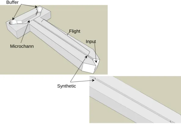
can be seen in Figure 2.1.
Figure 2.1 Computer assisted design image of the basic sensor geometry with
important structures labeled.
Synthetic pores
Flight Tube Buffer
Reservoirs
Microchann el
By fabricating a nanochannel with two nanopores embedded within it, we
can make time-of-flight measurements that allow us to interrogate and identify
molecular entities flowing through the nanochannel; the time-of-flight provides a
molecular identification due to the unique electrophoretic mobility of the particular
entity within a nanochannel. The key to implementing this identification modality is
to use a simple and robust technique to measure the mobility as a single molecule
electrophoretically travels through the flight tube. In this case, we will discuss the
use of in-plane synthetic nanopores positioned at the input and output ends of the
nanometer-scale flight tube that generates a resistive pulse due to carrier buffer ion
exclusion when the target molecule travels through the pores. Thus, the mobility is
measured from the known electric field strength and distance between the pores as
well as the measured time of travel between the pores.
The pores are essentially coulter counters placed in series, giving a signal at
each pore as well as a time-of-flight measurement as the molecule travels the fixed
distance between the two pores. By utilizing an electrical method for detection, we
are able to simplify the auxiliary hardware needed to run the system and also,
negate the need for labeling the molecule we are interrogating; a molecular label can
perturb the electrophoretic mobility of the target molecule.
The sensor will be placed at the end of our universal molecular processing
units (uMPS), creating the readout for the single molecules of interest. These
molecules will vary in size depending on the sample being analyzed and the
nucleotides that act as diagnostic biomarkers in stroke, cancer and other disease
states of interest. In most cases, these biomarkers will be labeled oligonucleotides
produced from our solid phase ligase detection reactions upstream of the sensor. In
order to provide measurements on the order of single molecules in a thermoplastic
micro-/nanofluidic chip with the sensitivity to identify distinct single molecular
species, a sensor had to be designed that utilized resistive pulse sensing technology
(the Coulter principle). As was previously discussed, resistive pulse technology was
selected as the modality for this application because of the ability to make these
structures in thermoplastics with high reproducibility and scalability. Additionally,
the external equipment (electronic components) required to drive and readout from
these sensors are much smaller than those required for optical systems.
It was decided that a time-of-flight sensor with two RPS regions separated by
a nano flight tube would be the basis for the nano-sensor for our systems. This
builds on work that has demonstrated the use of nanopores in the detection of
single molecules. The decision to use a time-of-flight type measurement gives the
user three useful data points with each particle measurement. One current pulse
when the particle passes through the first pore, a second pulse when it passes
through the second, and the time-of-flight information from the duration between
the two pulses. These three data points will allow for the ability to accurately
determine the identity of the molecule passing through the time of flight tube.
Additionally, this sensor must be easily fabricated in the same embossing step as the
rest of the chip geometry to make the production of such chips scalable. This means
ion beam milling process and nano-imprint lithography (NIL). Structures too
complicated or small for these processes would change our fabrication strategy and
increase the time and cost required to fabricate each device.
The first variables that were considered were simply those involving the size
of the nanochannel containing the time of flight sensor as well as the dimensions’ of
the features contained within this region. Perhaps the most important thing to
consider when thinking about this nanochannel in terms of resolution is the overall
length of the gap between the two nanopores. It was determined that a 100 micron
total channel length with 80 microns between the two pores should be a sufficient
starting dimension to achieve acceptable resolution of the single molecules passing
through the flight tube. This was decided based on average particle sizes that might
be seen in this sensor as well as the nano-electrophoresis studies done by other
members of the lab. A time-of-flight length of 80 microns will allow particles of
various sizes to be driven at a range of different voltages while still residing within
the flight tube long enough to distinguish between the two pulses. Another very
important consideration when designing this sensor was the possibility of
co-residence of molecules within the flight-tube. Co-co-residence will not be a large issue
with the type of diagnostic applications we are interested in, as the biomarker
populations are so small, however, it is still worth designing out of the system as
much as possible. Several strategies can be utilized to mitigate the risk of
co-residence occurring and fouling the data. The first is creating sufficiently small
initial “entry” pulse can be distinguished with 100% confidence from the second
“exit” pulse. The simplest example of this would be making the second constriction
2-3 times as long as the first. This would significantly alter the shape of the
waveform created by the molecule passing though the pore so that it would be
easily distinguished from the first pore’s signal. Understanding that all of these
variables can be easily adjusted to fit specific tasks utilizing certain molecular
species makes this a very powerful and adaptable sensor design.
2.2Resistive Pulse Sensing (RPS)
Many applications require the direct counting of particles on the microscopic
scale. For decades, the Coulter counter has been utilized as a device to perform this
functionality automatically and rapidly for particles suspended in an electrolyte
solution.24 As particles pass through a constriction, electrolytes are pushed out of
the volume, altering the resistance within the channel. This change is measureable,
directly related to the resistivity of the particle passing through the channel,
allowing for accurate counting and limited identification capabilities. To
understand these events we can look at Equation 1 (DeBlois and Bean) which
describes the resistive effects of a particle that is much smaller than the surrounding
channel, which is a good approximation for most applications. Equation 1 is given
as:
D
R
=
R
2-
R
1=
r
d
3where R2 is the resistance of pore with the particle inside it, R1 is the empty pore, ρ
is the resistivity of the particle, d is the diameter of the particle, and D is the
diameter of the pore. The change in resistance is proportional to the cube of the
diameter and inversely proportional to the fourth power of the pore diameter for
most applications.24 Additionally, some specific analytes require geometry
adjustments to better suit the actual physics occurring within the pore geometry.
For example a recent paper out of the Jacobson group describes the use of resistive
pulse technology for the discrimination of T=3 and T=4 HBV virus capsids. In order
to mathematically describe these capsids, the particle is treated as a porous
spherical shell, or a hollow “wiffle ball” geometry, filled with electrolyte.54 In the
case of the polystyrene bead experiments, such alterations may be necessary if the
simplified equations do not correspond well with experimental values. For ssDNA
measurements a “polymer chain” type geometry where multiple spheres pass
through the pore in series may be the best way to approximate the behavior and
physics of the oligonucleotide markers in solution.
2.3COMSOL Assisted Iterative Design
In working to develop a nanoscale time of flight sensor for the universal
molecular processing unit, an iterative design process was utilized in tandem with
COMSOL simulations to refine the geometry at each step. By utilizing two
nanopores in series in a nanochannel, we are able to harness the coulter principle
device, indicating that this strategy will be successful in thermoplastics with even
smaller channels and particles.54 Our device doesn’t need to achieve
mononucleotide resolution, but small oligonucleotide products will be the targets
identified in this sensor. This will eventually require structures on the order of 1-10
nanometers. However, it would be impractical to immediately begin by trying to
design and fabricate a microfluidic with structures on the order of only a few
nanometers. Accordingly, it was decided that a proof-of concept device with larger
dimensions (about 10X larger than the desired dimensions for the final device)
would be the ideal beginning step for this project.
Initially a two-dimensional single nanopore was created within a
nanochannel with the aid of computer assisted design software (AutoCAD 2014).
This 2D pore essentially assumes an infinitely flat circle with the same properties at
the particle moving through an infinitely flat channel with the same properties as
the three-dimensional fluidic channel. This single pore was then imported into
COMSOL Multiphysics 4.3 and utilized as a basic model to look at the behavior of the
electric field around the nanopore structure. This basic structure was then
extrapolated into a two-dimensional time-of-flight nanochannel with the two
nanopores separated by 100 micrometers. The nanochannel had a width of 100 nm
and the pores constricted to 50 nm. Additionally, an input funnel was included, as
previous work from Dr. Soper’s lab group had shown that input structures allowed
more particles to migrate into the nanochannel.55 An electric field was created
using a 10 volt driving potential from before the input funnel to the output fluidic
flow through the nano flight tube when it is embedded into a universal molecular
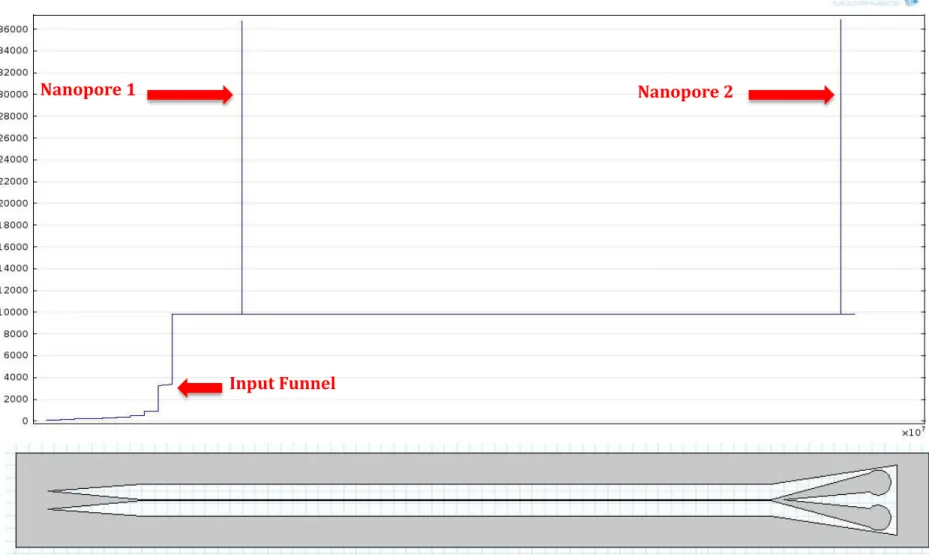
processing chip; that is to say, it will not be an isolated entity. Figure 2.2 shows the
imported nano flight tube geometry and the resulting electric field trace. This
simulation is very different from most of the others, as it had no flow considerations.
The voltage was simply applied to a conductive two-dimensional channel
22
Figure 2.2 Two-dimensional flight tube imported into COMSOL with electric field trace resulting from 10 V potential applied
through the center of the channel. This simulation was performed with a fine mesh and channel resistance with water.
Nanopore 1 Nanopore 2
A two dimensional model quickly became insufficient to understand the
properties of a true three-dimensional nanopores and not just a channel
constriction in one dimension. Again, initially a system with an input funnel and a
single nanopore was created for simplicity and simulation processing time. By
comparing the initial results from this model to that of the two-dimensional model
containing two pores, we found that this model could be accurately extrapolated
into a two-nanopore flight tube. This model had a nanochannel with a 100 nm X
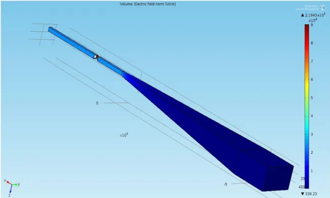
100 nm cross section and a 50 nm X 50 nm X 50 nm pore (Figure 2.3).
Figure 2.3 Initial three dimensional model with 50 nm pore and input funnel; a 10 V
potential was applied and the color chart represents the resulting electric field strength.
system. This model relies on the Coulter principle, or a resistive pulse
measurement, as it is more commonly named to in the literature. The current
blocking measurement is dependent upon how many ions the insulating particle
(polystyrene bead) can displace within the detecting volume (the nanopore). In the
case of this model, the 40 nm polystyrene bead displaces 33.5 zL of the 125 zL
detection volume. This is approaching an idealized situation, where the particle
takes up as much space in the detection volume as possible without risk of physical
blockage. Considering actual polystyrene nanobeads typically have a tolerance of ±
10% and nanochannel walls created by FIB milling often have a slope induced by the
Gaussian profile of a focused ion beam, this is the tightest fit that we could
confidently model. This yields a volume displacement of approximately 27%.
Fortunately, the volume displacement in the current blocking measurement isn’t the
only critical variable, the ionic strength of the buffer and the applied potential affect
the duration and magnitude of the signal generated by a particle passing through
the detection volume. These variables will have to be fine-tuned depending on what
size particles are being passed through the actual device and what their electrical
properties are.
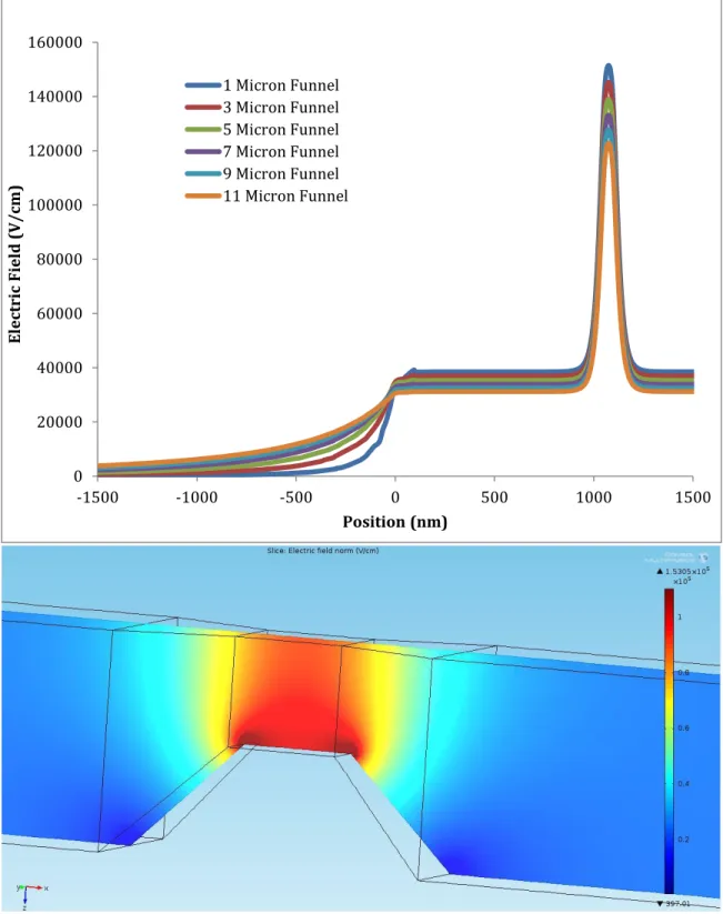
The first variable assessed with this model was the length of the input funnel.
Previous research has demonstrated that the geometry at the input of the channel
affected the rate at which particles enter the channel.55 However, we were also
interested in the effect the geometry has on the electric field, particularly across the
nanopore. This was investigated by keeping the overall length of the channel and
from 1 micron to 11 microns. Additionally, the boundary dimensions were held
constant: in all trials, the funnel sloped from a channel with dimensions of 2 μm X 1
μm to a channel with dimensions of 100 nm X 100 nm. The results from this
experiment can be seen in Figure 2.4, along with a close up view of the electric field
at the nanopore (indicating a lack of dead volume). A number of interesting findings
came from this experiment:
1) The funnel length drastically affects the slope of the electric field at the
transition region from the funnel to the nanochannel. The longer the
funnel, the less severe the rise in electric field strength. This will not only
affect the number of particles entering the nanochannel but also the rate
at which particles are entering the sensor.
2) The longer the input funnel, the lower the electric field strength at the
nanopore. This is very important when considering how rapidly a
particle will move through the detection region and the ability of the
Figure 2.4 Graph displaying results from input funnel length experiment in which the input funnel was varied from 1-11 μm and the channel size was held constant at 100 μm X 100 μm. A close-up of electric field at the nanopore is also provided to show the sharp rise seen on the graph.
0 20000 40000 60000 80000 100000 120000 140000 160000
-1500 -1000 -500 0 500 1000 1500
El
ect
ric
Fiel
d
(V
/cm
)
Position (nm) 1 Micron Funnel
The next experiment performed utilizing this model was a buffer
concentration experiment to understand how the buffer would affect not only the
baseline current recorded but also the change in current as a particle passed
through the detection nanopore. Tris-borate-EDTA (TBE) buffer was selected as the
buffer because of its prevalence in electrophoresis experiments, particularly those
involving nucleic acids. For this experiment the funnel length (10 microns), driving
potential (10 V), and pore geometry were all held constant. The TBE buffer
concentration was varied from 1.0X to 2.5X. The measurement was taken from the
simulation as the particle was in 11 different positions, but essentially we can think
of two conditions: a blocked condition, where the particle is centered in the
detection nanopore, and an unblocked condition, where the particle is in the larger
channel on either side of the nanopore. Table 2.1 shows the summarized results
from the modeled buffer experiment.
TBE
Concentration Conductivity (S/m) Current (nA)Empty Current (nA)Blocked Difference (nA) DifferencePercent
0.5X 0.576 19.17 18.53 0.64 3.35%
1.0X 0.901 29.98 28.98 1.00 3.35%
1.5X 1.083 36.04 34.83 1.21 3.35%
2.0X 1.389 46.22 44.68 1.55 3.35%
The TBE buffer experiment indicated that the TBE buffer concentration not only
changes the baseline current through the nano flight tube proportionally to the
conductivity of the buffer, but the current change when the pore is blocked is also
changed by this scale factor. This means that the highest buffer concentration
feasible in a physical device will give the highest amplitude signal at each nanopore.
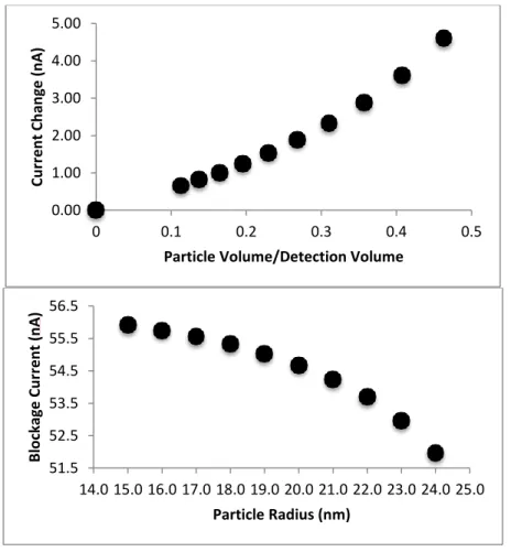
The final experiment performed utilizing this model was a study on the effect
of the particle size on the sensor response. This was a critical experiment for
understanding how the sensor would perform in a real setting where different
analyte molecules of varying sizes will be flowing through the sensor in one run.
Going back to the physics of the Coulter counter, this is very important because the
size of the particle determines how much conductive volume is being displaced.
This can be done through an experiment with two measurements, one in the
unblocked state and the other in the fully blocked state. The input funnel length,
buffer concentration, driving potential, and the sensor geometry were all held
constant for this simulation. The particle remained a sphere and always passed
directly through the center of the detection volume, but the radius of the sphere was
varied from 15 nm to 24 nm. This is not a practical experiment for a physical device
because of the variance in the polystyrene nanobeads; a COMSOL simulation is an
excellent way to understand the response of the sensor without risking blockage of
a test device. The sensor’s blockage current value exhibited a nonlinear response to
the particle diameter and the proportion of the detection volume blocked by the
particle. As would be expected, the greater the diameter of the particle, the greater
detection volume, as was stated previously. However, the increase was not linear,
but rather exponential as the blocked volume approached the total detection
volume of the nanopore. This behavior indicates that great care must be taken
when deciding upon the dimensions required for a specific application. Too large of
a pore and some smaller analytes may go undetected, too small of a pore and larger
molecules could potentially block the sensor. The results of this experiment can be
seen in Figure 2.5.
Figure 2.5 Results from the particle size simulation represented in two graphs. The
first examines the overall blocked current vs. particle radius, the second shows the current drop vs. the proportion of the detection volume filled by the particle. The
0.00 1.00 2.00 3.00 4.00 5.00
0 0.1 0.2 0.3 0.4 0.5
Cu rr e n t Ch an ge ( n A )
Particle Volume/Detection Volume
51.5 52.5 53.5 54.5 55.5 56.5
14.0 15.0 16.0 17.0 18.0 19.0 20.0 21.0 22.0 23.0 24.0 25.0
B lo ckage Cu rr e n t (nA )
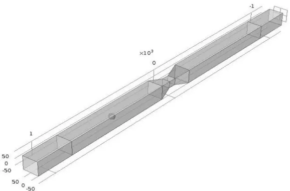
The final simulation utilized a new model with only a nanochannel and a
nanopore centered within it. Removing the input funnel and other extraneous
volumes allowed for faster simulation processing time as well as enhanced signal
measurements from the model with a much finer mesh. Again this model was
initially designed in AutoCAD 2014 and then imported into COMSOL 4.3; it can be
seen in Figure 2.6.
Figure 2.6 Model for nanopore length simulations in which finer meshes were used
to further understand the behavior of the particles and their signals as they passed through the pore.
The polystyrene bead can be seen in the first part of the nanochannel before
the pore. This bead was “stepped” through the nano flight tube and current
measurements were taken at 45 distinct points. This process was initially repeated
channel dimensions as well as the radius of the polystyrene sphere (20 nm) were
held constant, along with the buffer concentration (2.5X TBE) and driving potential
(10 V). It was found that the pore lengths closest to the particle diameter displayed
the largest current drop. Additionally, it was found that longer pores produce
longer signals, whereas shorter pores produce shorter signals. These results can be
seen in Figure 2.7.
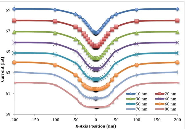
Figure 2.7 Simulation (COMSOL) results showing the effects of pore length on the
current response generated. A pore with a cross section of 50 nm X 50 nm was varied in length from 10 nm to 80 nm. For each length a polystyrene bead with a diameter of 40 nm was stepped through positions inside of the pore, the resultant drop in current was recorded.
59 61 63 65 67 69
-200 -150 -100 -50 0 50 100 150 200
Cu
rr
ent
(
nA
)
X-Axis Position (nm)
After obtaining data from this initial pore length experiment, we wanted to
refine the model further to better understand the relationship between the pore
length and the shape of the signal output from the sensor. The same geometry as
shown in Figure 2.6 was used but with a finer mesh, especially around the curvature
of the polystyrene sphere. Again, it was demonstrated that the lengths closest to the
diameter of the particle showed the largest current drop, with diminishing signals
as the pore length got much larger or smaller, as shown in Figure 2.8. The difference
in the width of the signal was also seen more clearly, further elucidating the idea
that the sensor geometry could be modified to match the hardware that is
performing the current measurements. For systems where the sampling frequency
limit is being approached, a longer pore could allow for more particles to be
correctly detected. Conversely, for systems where the dynamic range is the limiting
variable, a shorter pore, closer to the diameter of the particle, could be used to
ensure that the signal has the highest amplitude possible. This experiment further
aided in our understanding of the adaptability of this sensor design and the way it
30 53.4 53.6 53.8 54.0 54.2 54.4 54.6 54.8 55.0 55.2 700 1200 Cu rr ent (nA) Position (nm)
20 nm
51.2 51.4 51.6 51.8 52.0 52.2 52.4 52.6 52.8 53.0 700 1200 Cu rr ent (nA) Position (nm)50 nm
43.3 43.5 43.7 43.9 44.1 44.3 44.5 44.7740 940 1140 1340 1540
2.4 Fabrication of a Nano Time-of-Design Flight Sensor
Once the sensor geometry had been modeled and the variables affecting the
current blockage signal were better understood, it was time to begin fabrication of a
nano flight tube. We utilized a nanofabrication method that has been reported in
the literature.55,56 The first step in this process involved creating the
microstructures that serve as reservoirs and feed channels in a pure silicon wafer.
Two v-shaped access channels were patterned into a standard silicon <100> wafer
(University Wafers, Boston, MA) utilizing standard photolithography and
anisotropic etching with 50% KOH. These channels measured 55 μm wide by 12 μm
deep, and 1.5 cm long. All of this was completed in the UNC clean room.
The next step in this process was calibrating the input variables to the output
structures on the focused ion beam (FIB) (FEI Helios 600 Nanolab DualBeam
System). By milling structures and then analyzing and measuring them, we were
able to create a “calibration curve” for the channels milled by the FIB. At the same
time, 24-bit gradient bitmap files were created, which contained the desired
structures to be milled into the silicon wafer. A number of strategies were
attempted to achieve the optimal result. Finally, it was decided upon that the entire
nano flight tube would be milled in one ion exposure with the guidance of one
gradient bitmap image. This produced the most consistent results, minimized the
exposure of the silicon to ion and electron bombardment, and reduced the risk of
drift causing misalignment of structures. The final device was produced with a
structure successfully connected the two access microchannels and produced all of
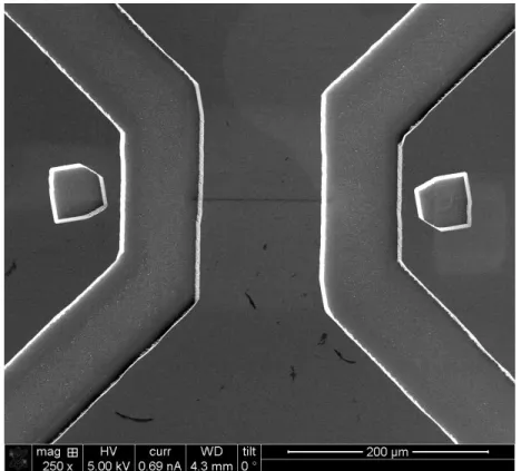
the features from the bitmap, shown in Figure 2.9.
Figure 2.9 Zoomed out SEM of nano flight tube between access microchannels in a
silicon wafer. The microchannels were produced with anisotropic wet etching techniques and the nanochannel was produced via FIB milling with a milling current of 9.7 pA, a dwell time of 1 μs, and a mill time of 5:24. (FEI Helios 600 Nanolab DualBeam System)
The next fabrication step involved the production of a resin stamp from the
silicon master so that the structures that have negative tone on the master can have
positive tone and be imprinted into thermoplastics. This is accomplished by first
silanizing the silicon master in a desiccator for 3 hours. A drop of a UV-curable resin
the surface of the silicon master and lightly pressed down with a scored piece of
6017 COC (Topas Advanced Polymers, Florence, KY) to serve as the backplate of the
stamp. Once all bubbles were removed and the resin had completely filled the
structures on the silicon master, the entire assembly was placed into a CL-100
Ultraviolet source and exposed to 365 nm (10 J/m2) UV light for 6 minutes to ensure
complete crosslinking of the resin and adhesion to the COC backplate. The assembly
was then removed and the now cured stamp was carefully demolded from the
silicon master.
Next, the structures in the stamp were or imprinted into a 1.5 mm thick
PMMA (Good Fellow, Berwyn, PA) substrate that would be the final chip containing
the nanochannel and nanopore. Imprinting was performed using a HEX03 from
JenOptik with a pressure of 1910 kN/m2 for 120 seconds. During the imprinting
step, the top and bottom platens were held at a temperature of 125 °C. Once the
imprinting step was complete, the platens were cooled to 40 °C and the pressure
was removed. The PMMA chip was then carefully demolded from the resin stamp
and four holes were drilled, one at each reservoir. After the holes were drilled and
all debris was removed from the chip, the PMMA substrate and a 8007 COC cover
plate were oxygen plasma treated for 2 minutes to clean the surfaces and decrease
their water contact angle. The substrate and cover plate were then pressed together
and sealed in an airtight vacuum bag to begin the bonding. The assembly was then
removed from the bag and placed between polyimide films and rubber sheets, and
then placed in the HEX03. Once the chamber closed, both platens were brought to
then cooled back to room temperature (~25 °C), and the pressure was slowly
removed from the device.
Once several devices had been imprinted and bonded, the stamp was
analyzed using atomic force microscopy (AFM) (Asylum Research MFP-3D Atomic
Force Microscope) in repulsive tapping mode at a rate of 0.5 Hz. A Tap300A1-G
cantilever tip was used with a force constant of 40 N/m and a frequency of 300kHz.
This allowed us to assess the fidelity of the stamp as well as measure the channels
being produced. From these scans, it was seen that the pore structures from the
bitmap were faithfully transferred not only to the silicon, but also to the resin stamp.
The AFM results are shown in Figure 2.10.
Figure 2.10 Three-dimensionally rendered AFM scan showing the pore structure
produced in the resin stamp. This particular stamp had nanochannels 50 nm deep with a 10 nm deep nanopore. This image was captured on an Asylum Research MFP-3D Atomic Force Microscope in repulsive tapping mode at a rate of 0.5 Hz. A Tap300A1-G cantilever tip was used with a force constant of 40 N/m and a
CHAPTER 3
Integrated Multiscale Module For Diagnostic Applications
3.1 Design Considerations and Requirements
A multiscale device needed to be designed that could carry out multiple solid
phase reactions on pillars, have individually addressable subpopulations on those
pillars, incorporate the time of flight sensor that was developed in the previous
chapter, and allow for re-interrogation to minimize the effects of mis-ligation errors.
By incorporating all of this functionality into one chip we can bring in genetic
material from the sample, interrogate it with ligase detection reactions and then
individually address these pillars by releasing their products into the time-of-flight
nanotubes. In order to accomplish this, a multiscale microfluidic module was
designed and modeled through an iterative process to create an efficient chip that
could accomplish all of the required tasks. More specifically, the chip will be able to:
1) Capture poly-T tailed targets using polymer pillars covalently loaded with
LDR primers
2) Carry out various molecular processing steps on the immobilized targets
3) Thermally release solid-phase ligase detection products from the pillar
arrays
4) Detect and identify single molecules using the time of flight nanosensor
5) Perform steps 2-4 multiple times to allow for re-interrogation of the
immobilized strands of interest on the pillar arrays
To accomplish all of the tasks required, various chip designs were considered
and modeled to understand their behavior. Some of the earlier designs revolved
around complex multi-layer devices with vacuum pumps pulling products and
waste out in the vertical axis. Another early design explored the idea of individually
addressable micro-heaters that would allow for very specific release of spLDR
products off of targeted pillars, allowing for products detected to be traced back to a
particular location on the chip. However, this design ran into limitations of
substrate thickness as well as increasing complexity due to the incredibly abundant
heat dissipation channels required to control the flux from the heaters. The design
that would turn into the final design presented in this thesis came from the idea of
individual pillar array, physically isolated from one another, each with their own
single molecule detector. In this way, like in the other designs, the precise location
on chip could be known and could be re-interrogated as is required for the
particular application.
3.2 Final Design
After an iterative design process that will be discussed further later, a final
design was developed that fulfills all off the design constraints and capabilities
Figure 3.1 Overview of the final chip design (410μm x 200μm). More details and structures labeled in Figure 3.10.
As can be seen in the final design, 8 nanosensors are placed in parallel within
a single chip. Each nanosensor has its own pillar “reaction bed” on which ligase
detection reactions can take place to identify and capture target biomarkers. All of
the important functionality of this chip will be discussed.
An important breakthrough that allowed this design to be feasible was the
notion of a hybrid drive system for the chip. In this hybrid system, all of the initial
genetic material for analysis is loaded on to the chip with hydrodynamic flow. Then,
once the target molecules have attached to the pillar arrays, the waste is pumped off
hydrodynamically. Finally, once the products are alone in the chip on the pillars,
they are released and driven electrophoretically into the nano time of flight tubes.
This novel scheme allowed for the pillars to be located so close together and for the
Once this final device was created in SolidWorks 2013, it was imported into
COMSOL so that important functions could be modeled and understood (COMSOL
was used at each design step as a way to verify). The first simulation that was
looked at was simply the hydrodynamic flow profile through the chip, essentially,
how would fluid move during the loading and waste removal stages. The resulting
flow profile can be seen in Figure 3.2.
Figure 3.2 Steady-state hydrodynamic flow profile through the entire chip
Next, we focused in on the regions that are critical to the device functioning. Figure
3.3 shows that flow is uniform through the pillars and that the hydrodynamic
resistance of the nano flight tube is approaching infinity so that no material will
enter the tube when the chip is being actuated via hydrodynamic flow. The exact
capture efficiency of the pillar array will depend on the length of the particles being
flowed through the reactor, but the uniform pressure drop indicates uniform
capture distribution across the array.
Figure 3.3 Hydrodynamic flow profile at the critical elements of the chip. Again, a 1
The next experiment performed on this design in COMSOL evaluated the
Chevron baffles placed at the entrance. As can be seen in Figure 4.5, these chevrons
do a good job of splitting the flow into five streams spaced across the width of the
chip, rather than a single stream moving straight through the middle. However, the
flow profile is not nearly as interesting as the particle trajectories when they meet
the chevrons. The intent of the chevrons is to split the flow in such a way that each
pillar array has an equal chance of receiving particles. In this way not only the
center arrays will receive samples, we want to make sure the entire surface area of
the pillar arrays is utilized as much as possible. A movie was generated from this
simulation, showing the particles in motion, however, the still image of the
trajectories tells the story well enough, Figure 3.4.
Figure 3.4 Particle traces through second generation design device taken from a
The final simulation involved the offloading of product from the pillars into
the flight tubes for analysis. In these experiments no hydrodynamic pumping was
occurring, only the electrokinetic movement generated by the potential applied at
the entrance to the chip with ground connections at the reservoir of each individual
nano flight tube. Figures 3.5 shows the electric field across the entire chip. Figure
3.6 shows the electric field only at the critical areas, indicating that when the electric
field is turned on, all biomarker targets released from the pillar arrays will flow into
the detection tubes and not out into waste beyond the sensors. The importance of
this feature cannot be overstated. When working with extremely rare molecules,
single counts can make a difference.
Figure 3.5 Electric field across entire chip, strength is proportional to arrow
Figure 3.6 Electric field lines at the critical area of the detection chip. All arrows are converging into the flight tube, creating an electrical boundary between individual pixels and flight-tubes. This design should minimize any chance of cross-talk between the sensors.
3.3 An Iterative Design Process
Initial designs varied greatly and looked markedly different from the final
design that was presented, suggesting the power of an iterative process to optimize
a design application. Successful design elements from early models were combined,
and outputs in four directions, and individually addressable heaters. An example of
one such design can be seen in Figure 3.7.
Figure 3.7 Earliest design of multiscale device.
During the modeling of this design, it was quickly realized that the design
was too complicated to be reproducible and scalable, the inputs and outputs from
multiple directions would have required much more external equipment and the
heater placement would have required multi-level channels with precise alignment.
As was already discussed, the individually addressed heaters in close proximity had
insurmountable challenges to a functional device. An example of this heat flux
problem can be seen in Figure 3.8, the values associated with the heat waves are not
as important as the fact that they propagate despite the thermal isolation grooves
center of the middle pillar array and terminate at the isolation grooves on either
side, allowing for precise release off of each individual pillar array. This was simply
not possible in the thermoplastics that we were interested in using for this
application.
Figure 3.8 Heat model of individually addressable heater with thermal isolation
grooves. This illustrates the challenge that despite including many heat mitigation and isolation techniques (see grooves and staggering), the heater beneath each pixel simply radiated too much heat to the surrounding pixels, making precise control of the thermal release impossible.
Building from this knowledge set secured from previous designs, a new
device architecture was developed that addresses operational issues evident from
this type of design, multiple pillar arrays shared 1 detector. An example can be seen
in Figure 3.9.
Figure 3.9 Second generation design with unidirectional flow and individual
heaters. This design was a “stepping stone” to the ideas present in the final design and was not simulated extensively.
Second generation designs were modeled extensively, and had a lot of really
nice properties, however, the individually addressable heaters remained the failing
point, with thermal isolation being impossible if enough heat was going to make it
through the substrate to interact with the molecules attached to the pillar arrays.
The third generation built upon these designs and incorporated some new elements
as well. These devices will be configured with a number of fluidic chambers that are
comprised of Chevron baffles to allow uniform addressing of 8 pixels (20 x 20 µm; 1
µm x 5 µm pillars; 288 pillars per pixel) and a nanochannel flight tube situated at the
output end of each pixel (as described in Chapter 2). As shown and discussed
Figure 3.10 Final device design, looking from the entrance down the module as well as a zoomed in view with important features labeled. This design incorporates many of the elements from the previous designs.
This chapter illustrates the design path that was taken to fulfill the design
parameters given to me by my lab group for the chip’s use in the modular molecular
processing device. By using an iterative process all of the best attributes from each
design were included in future designs while detrimental elements were excluded.
This design will likely need to be fine-tuned further to the individual requirements
necessary for unique diagnostic applications. However, the basic design will be
extremely flexible and useful for many applications. By utilizing a straight-through
flow (1 input, 1 output), this can be placed in series in any fluidic circuit. The
Chevron Baffles Nanoscale
Flight Tubes
Fluidic Input
Single Pixel (Pillars) To Waste Electrical
CHAPTER 4
Conclusion
This thesis outlines the work done for my master’s project. This project
combined engineering, chemistry, and some biology in order to understand the
design requirements for these two critical components of the universal molecular
processing system that Dr. Soper’s research group is working on creating.
The time-of-flight sensor that was designed utilizes two nanopores in series
to create two regions of resistive pulse sensing. This design scheme should give
excellent sensitivity by leveraging three distinct measurements while mitigating a
lot of potential disadvantages from co-residence issues and fabrication difficulty.
COMSOL simulations were utilized to guide our design and optimize the parameters
of the sensor, allowing us to iterate over many variables without wasting resources
on fabricating failed devices. These experiments were included in this report to
demonstrate the design process.
The integrated multiscale module built upon the time of flight sensor we
designed and added in the previous processing step as well as the modality for
isolating and controlling what flows into the sensor. By utilizing multiple sensors on
one module we were also able to make this system re-addressable, helping to deal
with the problem of mis-ligation events when working with ligating enzymes. This
hydrodynamic flow, which loads the pillars, carries out the reaction, and then
removes the waste. The second flow profile is the electrokinetic, which drives the
ligation products into the time-of-flight sensors for analysis.
Some fabrication was completed on a proof-of-concept time-of-flight sensor;
however, fabrication will be the main next steps for these devices. Despite following
fabrication strategies used in other areas of our work, there will certainly be
challenges associated with fabricating these devices. Fortunately, these devices can
be easily made on different length scales and still function, so some fabrication
issues may be avoided simply by scaling the devices correctly for specific
applications.
REFERENCES
(1) Yager, P.; Edwards, T.; Fu, E.; Helton, K.; Nelson, K.; Tam, M. R.; Weigl, B. H.
Nature2006, 442, 412–418.
(2) Feigin, V. L.; Lawes, C. M.; Bennett, D. a.; Barker-Collo, S. L.; Parag, V. Lancet Neurol.2009, 8, 355–369.
(3) Norris, J. W.; Hachinski, V. C. Lancet1982, 1, 328–331.
(4) Goldstein, L. B. Stroke2005, 293, 2391–2402.
(5) Baird, a E. Biochem. Soc. Trans.2006, 34, 1313–1317.
(6) Pullagurla, S. R.; Witek, M. A.; Jackson, J. M.; Lindell, M. A. M.; Hupert, M. L.; Nesterova, I. V; Baird, A. E.; Soper, S. A. Anal. Chem.2014, 86, 4058–4065.
(7) Moerner, W. E.; Ambrose, W. P. Phys. Rev. Lett.1991, 66, 1376.
(8) Brooks Shera, E.; Seitzinger, N. K.; Davis, L. M.; Keller, R. A.; Soper, S. A. Chem. Phys. Lett.1990, 174, 553–557.
(9) Trautman, J. K.; Macklin, J. J.; Brus, L. E.; Betzig, E. Nature1994, 369, 40–42.
(10) Funatsu, T.; Harada, Y.; Tokunaga, M.; Saito, K.; Yanagida, T. Imaging of single fluorescent molecules and individual ATP turnovers by single myosin
molecules in aqueous solution. Nature, 1995, 374, 555–559.
(11) Ishii, Y.; Yanagida, T. Single Mol.2000, 1, 5–16.
(12) Zander, C.; Drexhage, K. H.; Han, K.-T.; Wolfrum, J.; Sauer, M. Chem. Phys. Lett. 1998, 286, 457–465.
(13) Lyon, W. a; Nie, S. M. Anal. Chem.1997, 69, 3400–3405.
(14) Dickson RM, Norris DJ, TzengYL, M. W. Science (80-. ).1996, 8.
(15) Information, S.; Emory, J. M.; Peng, Z.; Young, B.; Hupert, M. L.; Rousselet, A.; Patterson, D.; Ellison, B.; Soper, S. A.; Rouge, B. 2011.
(16) Holland, C. a.; Kiechle, F. L. Curr. Opin. Microbiol.2005, 8, 504–509.
(17) Fan, Y.; Chen, X. T.; Tung, C. H.; Kong, J. M.; Gao, Z. Q. TRANSDUCERS