IPC-A-610E
This redline document is to help users see
significant changes from Revision D.
New or changed text are shown in blue and underlined like this.
Deleted or moved text is shown in red and strikethrough like this.
Changes from Revision D to Revision E; references in the figure boxes refer to the source picture or indicate if a new picture is being used. Clause number changes as a result of reorganizing within this chapter are not shown.
1 Forward
The following topics are addressed in this section: 1.1 Scope
1.2 Purpose 1.3 Classification
1.4 Definition of Requirements 1.4.1 Acceptance Criteria 1.4.1.1 Target Condition 1.4.1.2 Acceptable Condition 1.4.1.3 Defect Condition 1.4.1.3.1 Disposition
1.4.1.4 Process Indicator Condition 1.4.1.4.1 Process Indicator Methodologies 1.4.1.5 Combined Conditions
1.4.1.6 Conditions Not Specified 1.4.1.7 Specialized Designs 1.5 Terms & Definitions 1.5.1 Board Orientation 1.5.1.1 *Primary Side 1.5.1.2 *Secondary Side 1.5.1.3 Solder Source Side 1.5.1.4 Solder Destination Side 1.5.2 *Cold Solder Connection 1.5.3 Electrical Clearance 1.5.4 High Voltage 1.5.5 Intrusive Solder 1.5.6 *Leaching
1.5.7 Meniscus (Component) 1.5.8 *Nonfunctional Land 1.5.9 Pin-in-Paste
1.5.10 Wire Diameter 1.5.11 Wire Overwrap 1.5.12 Wire Overlap
1.6 Examples and Illustrations 1.7 Inspection Methodology 1.8 Verification of Dimensions 1.9 Magnification Aids 1.10 Lighting
If a conflict occurs between the English and translated versions of this document, the English version will take precedence.
1.1 Scope
This standard is a collection of visual quality acceptability requirements for electronic assemblies.
This document presents acceptance requirements for the manufacture of electrical and electronic assemblies. Historically, electronic assembly standards contained a more comprehensive tutorial addressing principles and techniques. For a more complete understanding of this document's recommendations and requirements, one may use this document in conjunction with IPC-HDBK-001, IPC-AJ-820 and IPC J-STD-001.
The criteria in this standard are not intended to define processes to accomplish assembly operations nor is it intended to authorize repair/modification or change of the customer’s product. For instance, the presence of criteria for adhesive bonding of components does not imply/authorize/require the use of adhesive bonding, the depiction of a lead wrapped clockwise around a terminal does not imply/authorize/require that all leads/wires be wrapped in the clockwise direction.
Users of this standard should be knowledgeable of the applicable requirements of the document and how to apply them. Objective evidence of the demonstration of this knowledge should be maintained. Where objective evidence is unavailable, the organization should consider periodic review of personnel skills to determine visual acceptance criteria appropriately. IPC-A-610 has criteria outside the scope of IPC J-STD-001 defining handling, mechanical and other workmanship requirements. Table 1-1 is a summary of related documents.
IPC-AJ-820 is a supporting document that provides information regarding the intent of this specification content and explains or amplifies the technical rationale for transition of limits through Target to Defect condition criteria. In addition, supporting information is provided to give a broader understanding of the process considerations that are related to performance but not commonly distinguishable through visual assessment methods.
The explanations provided in IPC-AJ-820 should be useful in determining disposition of conditions identified as Defect, processes associated with Process Indicators, as well as answering questions regarding clarification in use and application for defined content of this specification. Contractual reference to IPC-A-610 does not additionally impose the content of IPC-AJ-820 unless specifically referenced in contractual documentation.
1.2 Purpose
The visual standards in this document reflect the requirements of existing IPC and other applicable specifications. In order for the user to apply and use the content of this document, the assembly/product should comply with other existing IPC requirements, such as IPC-7351, IPC-2220 (Series), IPC-6010 (Series) and IPC-A-600. If the assembly does not comply with these or with equivalent requirements, the acceptance criteria shall be defined between the customer and supplier.
The illustrations in this document portray specific points noted in the title of each page. A brief description follows each illustration. It is not the intent of this document to exclude any acceptable procedure for component placement or for applying flux and solder used to make the electrical connection; however, the methods used shall produce completed solder
Changes from Revision D to Revision E; references in the figure boxes refer to the source picture or indicate if a new picture is being used. Clause number changes as a result of reorganizing within this chapter are not shown.
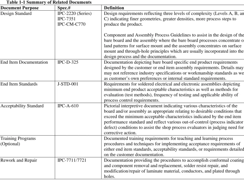
Table 1-1 Summary of Related Documents
Document Purpose Spec.# Definition
Design Standard IPC-2220 (Series) IPC-7351
IPC-CM-C770
Design requirements reflecting three levels of complexity (Levels A, B, and C) indicating finer geometries, greater densities, more process steps to produce the product.
Component and Assembly Process Guidelines to assist in the design of the bare board and the assembly where the bare board processes concentrate on land patterns for surface mount and the assembly concentrates on surface mount and through-hole principles which are usually incorporated into the design process and the documentation.
End Item Documentation IPC-D-325 Documentation depicting bare board specific end product requirements designed by the customer or end item assembly requirements. Details may or may not reference industry specifications or workmanship standards as well as customer’s own preferences or internal standard requirements.
End Item Standards J-STD-001 Requirements for soldered electrical and electronic assemblies depicting minimum end product acceptable characteristics as well as methods for evaluation (test methods), frequency of testing and applicable ability of process control requirements.
Acceptability Standard IPC-A-610 Pictorial interpretive document indicating various characteristics of the board and/or assembly as appropriate relating to desirable conditions that exceed the minimum acceptable characteristics indicated by the end item performance standard and reflect various out-of-control (process indicator or defect) conditions to assist the shop process evaluators in judging need for corrective action.
Training Programs (Optional)
Documented training requirements for teaching and learning process procedures and techniques for implementing acceptance requirements of either end item standards, acceptability standards, or requirements detailed on the customer documentation.
Rework and Repair IPC-7711/7721 Documentation providing the procedures to accomplish conformal coating and component removal and replacement, solder resist repair, and
modification/repair of laminate material, conductors, and plated through holes.
1.3 Classification
Accept and/or reject decisions shall be based on applicable documentation such as contracts, drawings, specifications, standards and reference documents. Criteria defined in this document reflect three classes, which are as follows: Class 1 -- General Electronic Products
Includes products suitable for applications where the major requirement is function of the completed assembly. Class 2 -- Dedicated Service Electronic Products
Includes products where continued performance and extended life is required, and for which uninterrupted service is desired but not critical. Typically the end-use environment would not cause failures.
Class 3 -- High Performance Electronic Products
Includes products where continued high performance or performance-on-demand is critical, equipment downtime cannot be tolerated, end-use environment may be uncommonly harsh, and the equipment must function when required, such as life support or other critical systems.
1.4 Definition of Requirements
This document provides acceptance criteria for completed electronic assemblies. Where a requirement is presented that cannot be defined by the acceptable, process indicator, and defect conditions, the word "shall" is used to identify the
requirement. The word "shall" in this document invokes a requirement for manufacturers of all classes or product, and failure to comply with the requirement is a noncompliance to this standard.
All products shall meet the requirements of the assembly drawing(s)/ documentation and the requirements for the applicable product class specified herein. Missing hardware or components are a Defect for all classes.
1.4.1 Acceptance Criteria
When IPC-A-610 is cited or required by contract as a stand-alone document for inspection and/or acceptance, the requirements of IPC J-STD-001 "Requirements for Soldered Electrical and Electronic Assemblies" do not apply unless separately and specifically required.
When this standard is contractually required, the applicable requirements of this standard (including product Class –see 1.4.1) shall be imposed on all applicable subcontracts.
In the event of conflict, the following order of precedence applies: 1. Procurement as agreed and documented between customer and supplier.
2. Master drawing or master assembly drawing reflecting the customer’s detailed requirements. 3. When invoked by the customer or per contractual agreement, IPC-A-610.
When documents other than IPC-A-610 are cited, the order of precedence shall be defined in the procurement documents. Criteria are given for each class in four levels of acceptance: Target Condition, Acceptable Condition, and either Defect Condition or Process Indicator Condition.
1.4.1.1 Target Condition
A condition that is close to perfect/preferred, however, it is a desirable condition and not always achievable and may not be necessary to ensure reliability of the assembly in its service environment.
1.4.1.2 Acceptable Condition
This characteristic indicates a condition that, while not necessarily perfect, will maintain the integrity and reliability of the assembly in its service environment.
1.4.1.3 Defect Condition
A defect is a condition that may be insufficient to ensure the form, fit or function of the assembly in its end use environment. Defect conditions shall be dispositioned by the manufacturer based on design, service, and customer requirements.
Disposition may be to rework, repair, scrap, or use as is. Repair or "use as is" may require customer concurrence. A defect for Class 1 automatically implies a defect for Class 2 and 3. A defect for Class 2 implies a defect for Class 3. 1.4.1.3.1 Disposition
The determination of how defects should be treated. Dispositions include, but are not limited to, rework, use as is, scrap or repair.
Changes from Revision D to Revision E; references in the figure boxes refer to the source picture or indicate if a new picture is being used. Clause number changes as a result of reorganizing within this chapter are not shown.
1.4.1.4.1 Process Indicator Methodologies
Process control methodologies should be used in the planning, implementation and evaluation of the manufacturing processes used to produce soldered electrical and electronic assemblies. The philosophy, implementation strategies, tools and
techniques may be applied in different sequences depending on the specific company, operation, or variable under consideration to relate process control and capability to end product requirements. The manufacturer needs to maintain objective evidence of a current process control/continuous improvement plan that is available for review.
1.4.1.5 Combined Conditions
Cumulative conditions shall be considered in addition to the individual characteristics for product acceptability even though they are not individually considered defective. The significant number of combinations that could occur does not allow full definition in the content and scope of this specification but manufacturers should be vigilant for the possibility of combined and cumulative conditions and their impact upon product performance.
Conditions of acceptability provided in this specification are individually defined and created with separate consideration for their impact upon reliable operation for the defined production classification. Where related conditions can be combined, the cumulative performance impact for the product may be significant; e.g., minimum solder fillet quantity when combined with maximum side overhang and minimum end overlap may cause a significant degradation of the mechanical attachment integrity. The manufacturer is responsible for identification of such conditions.
1.4.1.6 Conditions Not Specified
Conditions that are not specified as defective or as a process indicator may be considered acceptable unless it can be established that the condition affects user defined form, fit or function.
1.4.1.7 Specialized Designs
IPC-A-610, as an industry consensus document, cannot address all of the possible components and product design combinations. Where uncommon or specialized technologies are used, it may be necessary to develop unique acceptance criteria. However, where similar characteristics exist, this document may provide guidance for product acceptance criteria. Often, unique definition is necessary to consider the specialized characteristics while considering product performance criteria. The development should include customer involvement or consent. For Class 3 the criteria shall include agreed definition of product acceptance.
Whenever possible these criteria should be submitted to the IPC Technical Committee to be considered for inclusion in upcoming revisions of this standard.
1.5 Terms & Definitions
Items noted with an * are quoted from IPC-T-50. 1.5.1 Board Orientation
The following terms are used throughout this document to determine the board side.: The source/destination side shall be considered when applying some criteria, such as that in Tables 7-4, 7-5 and 7-7.
1.5.1.1 *Primary Side
That side of a packaging and interconnecting structure (PCB) that is so defined on the master drawing. (It is usually the side that contains the most complex or the most number of components. This side is sometimes referred to as the component side or solder destination side in through-hole mounting technology.)
1.5.1.2 *Secondary Side
That side of a packaging and interconnecting structure (PCB) that is opposite the primary side. (This side is sometimes referred to as the solder side or solder source side in through-hole mounting technology.)
1.5.1.4 Solder Destination Side
The solder destination side is that side of the PCB that the solder flows toward in a through-hole application. The destination is normally the primary side of the PCB when wave, dip or drag soldering is used. The destination side may be the secondary side of the PCB when hand-soldering operations are conducted. The source/destination side must be considered when applying some criteria, such as that in Tables 7-3, 7-6 and 7-7.
1.5.2 *Cold Solder Connection
A solder connection that exhibits poor wetting and that is characterized by a grayish porous appearance. (This is due to excessive impurities in the solder, inadequate cleaning prior to soldering, and/or the insufficient application of heat during the soldering process.)
1.5.3 Electrical Clearance
Throughout this document the minimum spacing between non-common uninsulated conductors (e.g., patterns, materials, hardware, or residue) is referred to as “minimum electrical clearance.” It is defined in the applicable design standard or on the approved or controlled documentation. Insulating material needs to provide sufficient electrical isolation. In the absence of a known design standard use Appendix A (derived from IPC-2221). Any violation of minimum electrical clearance is a defect condition for all classes.
1.5.4 High Voltage
The term “high voltage” will vary by design and application. The high voltage criteria in this document are only applicable when specifically required in the drawings/procurement documentation.
1.5.5 Intrusive Solder
A process in which the solder paste for the through-hole components is applied using a stencil or syringe to accommodate through-hole components that are inserted and reflow-soldered together with the surface-mount components.
1.5.6 *Leaching
The loss or removal of a basis metal or coating during a soldering operation. 1.5.7 Meniscus (Component)
Sealant or encapsulant on a lead, protruding from the seating plane of the component. This includes materials such as ceramic, epoxy or other composites, and flash from molded components.
1.5.8 *Nonfunctional Land
A land that is not connected electrically to the conductive pattern on its layer. 1.5.9 Pin-in-Paste
See Intrusive Solder 1.5.10 Wire Diameter
In this document, wire diameter (D) is the overall diameter of conductor including insulation. Unless otherwise specified, criteria in this standard are applicable for solid wire/component leads or stranded wire.
1.5.11 Wire Overwrap
When a wire/lead that is wrapped more than 360° and remains in contact with the terminal post, Figure 6-64A. 1.5.12 Wire Overlap
Changes from Revision D to Revision E; references in the figure boxes refer to the source picture or indicate if a new picture is being used. Clause number changes as a result of reorganizing within this chapter are not shown.
1.7 Inspection Methodology
Accept and/or reject decisions shall be based on applicable documentation such as contract, drawings, specifications and referenced documents.
The inspector does not select the class for the assembly under inspection, see 1.3. Documentation that specifies the applicable class for the assembly under inspection shall be provided to the inspector.
Automated Inspection Technology (AIT) is a viable alternative to visual inspection and complements automated test equipment. Many of the characteristics in this document can be inspected with an AIT system. IPC-AI-641 "User's
Guidelines for Automated Solder Joint Inspection Systems" and IPC-AI-642 "User's Guidelines for Automated Inspection of Artwork, Inner-layers, and Unpopulated PCBs" provide more information on automated inspection technologies.
If the customer desires the use of industry standard requirements for frequency of inspection and acceptance, J-STD-001 is recommended for further soldering requirement details.
1.8 Verification of Dimensions
The actual measurements provided in this document (i.e., specific part mounting and solder fillet dimensions and
determination of percentages) are not required except for referee purposes. All dimensions in this standard are expressed in SI (System International) units (with Imperial English equivalent dimensions provided in brackets). All specified limits in this standard are absolute limits as defined in ASTM E29.
1.9 Magnification Aids and Lighting
For visual inspection, some individual specifications may call for magnification aids for examining printed board assemblies. The tolerance for magnification aids is ± 15% of the selected magnification power. Magnification aids, if used for inspection, shall be appropriate with the item being inspected. Unless magnification requirements are otherwise specified by contractual documentation, the magnifications in Table 1-2 and Table 1-3 are determined by the item being inspected.
Referee conditions are used to verify product rejected at the inspection magnification power. For assemblies with mixed land widths, the greater magnification may be used for the entire assembly.
Table 1-2 Inspection Magnification (Land Width)
Magnification Power Land Widths or Land Diameters1
Inspection Range Maximum Referee
> 1.0 mm [0.0394 in] 1.5X to 3X 4X
>0.5 to ≤1.0 mm [0.0197 to 0.0394 in] 3X to 7.5X 10X ≥0.25 to ≤0.5 mm [0.00984 to 0.0197 in] 7.5X to 10X 20X
< 0.25 mm 0.00984 in] 20X 40X
Note 1: A portion of a conductive pattern used for the connection and/or attachment of components. Table 1-3 Magnification Aid Applications – Other
Cleanliness (with or without cleaning processes) Magnification not required, see Note 1 Cleanliness (no-clean processes per 10.4.4) Note 1
Conformal Coating/Encapsulation Notes 1,2
Marking Note 2
Other (Component and wire damage, etc.) Note 1
1.10 Lighting
Lighting shall be adequate for the item being inspected.
Illumination at the surface of workstations should be at least 1000 lm/m2 [approximately 93 foot candles]. Light sources should be selected to prevent shadows.
Note: In selecting a light source, the color temperature of the light is an important consideration. Light ranges from 3000-5000° K enable users to distinguish various printed circuit assembly features and contaminates with increased clarity.
Changes from Revision D to Revision E; references in the figure boxes refer to the source picture or indicate if a new picture is being used. Clause number changes as a result of reorganizing within this chapter are not shown.
©Copyright 2010. IPC, Bannockburn, Illinois. All rights reserved under both international and Pan-American copyright conventions. Any copying, scanning or other reproduction of these materials without the prior written consent of the copyright holder is strictly prohibited and constitutes infringement under the Copyright Law of the United States.
3 Handling Electronic Assemblies
This chapter provides general guidelines and there were only minor editorial changes to help with understanding. There are no changes in criteria.
©Copyright 2010. IPC, Bannockburn, Illinois. All rights reserved under both international and Pan-American copyright conventions. Any copying, scanning or other reproduction of these materials without the prior written consent of the copyright holder is strictly prohibited and constitutes infringement under the Copyright Law of the United States.
4 Hardware
This section illustrates several types of hardware used to mount electronic devices to a printed circuit assembly (PCA) or any other types of assemblies requiring the use of any of the following: screws, bolts, nuts, washers, fasteners, clips, component studs, tie downs, rivets, connector pins, etc. This section is primarily concerned with visual assessment of proper securing (tightness), and also with damage to the devices, hardware, and the mounting surface that can result from hardware mounting.
Compliance to torque requirements is to be verified as specified by customer documentation. The verification procedure ensures that no damage to components or assembly occurs. Where torque requirements are not specified, follow standard industry practices.
Process documentation (drawings, prints, parts list, build process) will specify what to use; deviations need to have prior customer approval.
Note: Criteria in this section do not apply to attachments with self-tapping screws. Visual inspection is performed in order to verify the following conditions: a. Correct parts and hardware.
b. Correct sequence of assembly.
c. Correct security and tightness of parts and hardware. d. No discernible damage.
e. Correct orientation of parts and hardware. The following topics are addressed in this section: 4.1 Hardware Installation
4.1.1 Electrical Clearance 4.1.2 Interference 4.1.3 Heatsinks
4.1.3.1 Insulators and Thermal Compounds 4.1.3.2 Contact
4.1.4 Threaded Fasteners 4.1.4.1 Torque
4.1.4.2 Wires
4.2 Jackpost Mounting 4.3 Connector Pins
4.3.1 Edge Connector Pins 4.3.2 Press Fit Pins 4.3.2.1 Soldering
4.4 Wire Bundle Securing
4.4.1 General 4.4.2 Lacing
4.4.2.1 Lacing- Damage
4.5 Routing
4.5.1 Wire Crossover 4.5.2 Bend Radius 4.5.3 Coaxial Cable
4.5.4 Unused Wire Termination 4.5.5 Ties over Splices and Ferrules
Changes from Revision D to Revision E; references in the figure boxes refer to the source picture or indicate if a new picture is being used. Clause number changes as a result of reorganizing within this chapter are not shown.
4.1 Hardware Installation
4.1.1 Hardware Installation - Electrical Clearance Also see 1.5.31.4.5.
Acceptable - Class 1, 2, 3
• Spacing between noncommon conductors does not violate specified minimum electrical clearance (3). This is shown in Figure 4-1 as the distances between (1) & (2) and (1) & (5).
Defect - Class 1, 2, 3
• Hardware reduces spacing to less than specified minimum electrical clearance.
4.1.2 Hardware Installation - Interference
Acceptable – Class 1, 2, 3
• Mounting area clear of obstructions to assembly requirements.
Defect - Class 1, 2, 3
• Excess solder (uneven) on mounting holes where mechanical assembly will be affected.
• Anything that interferes with mounting of required hardware.
Figure 4-1 610D-04-001 1. Metallic hardware 2. Conductive pattern
3. Specified minimum electrical clearance 4. Mounted component
5. Conductor
Figure 4-2 610D-04-002 1. Metallic hardware 2. Conductive pattern
3. Specified minimum electrical clearance 4. Mounted component
5. Conductor
4.1.3 Heatsinks <moved here from 610D 7.2, damaged heat sink moved to 9.12> 4.1.3.1 Heatsinks - Insulators and Thermal Compounds
This section illustrates various types of heatsink mounting. Bonding with thermally conductive adhesives may be specified in place of hardware.
Visual inspection includes hardware security, component damage, and correct sequence of assembly. The following additional issues need to shall be considered:
• The component has good contact with the heatsink.
• The hardware secures the component to the heatsink.
• The component and heatsink are flat and parallel to each other.
• The thermal compound/insulator (mica, silicone grease, plastic film, etc.) is applied properly. Target - Class 1,2,3
• Uniform border of mica, plastic film or thermal compound showing around edges of component.
Acceptable - Class 1,2,3
• Not uniform but evidence of mica, plastic film or thermal compound showing around edges of component.
Defect - Class 1,2,3
• No evidence of insulating materials, or thermal compound (if required).
• Thermal compound precludes formation of required solder connection.
Figure 4-4 610D-7-52
Figure 4-5 610D-7-53
Changes from Revision D to Revision E; references in the figure boxes refer to the source picture or indicate if a new picture is being used. Clause number changes as a result of reorganizing within this chapter are not shown.
4.1.3.2 Heatsink - Contact
Target - Class 1,2,3
• Component and heatsink are in full contact with the mounting surface.
• Hardware meets specified attachment requirements.
Acceptable - Class 1,2,3
• Component not flush.
• Minimum 75% contact with mounting surface. • Hardware meets mounting torque requirements if
specified.
Defect - Class 1,2,3
• Component has less than 75% contact with mounting surface.
• Hardware is loose.
4.1.44.1.3 Hardware Installation - Threaded Fasteners
A minimum of one and one half threads need to extend beyond the threaded hardware, (e.g., nut) unless otherwise specified by engineering drawing. Bolts or screws may be flush with the end of the threaded hardware only where threads could interfere with other components or wires and when locking mechanisms are used.
Thread extension should not be more than 3 mm [0.12 in] plus one and one-half threads for bolts or screws up to 25 mm [0.984 in] long or more than 6.3 mm [0.248 in] plus one and one-half threads for bolts or screws over 25 mm [0.984 in]. This is providing that the extension does not interfere with any adjacent part and that the designed electrical clearance
requirements are met.
Both the order and orientation of mounting hardware need to be considered during assembly. Devices such as “star” or “tooth” washers may have one side with sharp edges intended to cut into the mating surface to keep the hardware from coming loose in operation. Figure 4-11 is an example of this kind of lock washer. Unless otherwise specified the sharp edges of the lock washer should be against the flat washer.
Acceptable - Class 1, 2, 3
• Proper hardware sequence and orientation. Figures 4-10 and 4-11.
• Slot or hole are is covered with flat washer, Figure 4-12.
• Hole is covered with flat washer, Figure 4-5.
Figure 4-7 610D-7-55 1. Heat sink
Figure 4-8 610D-7-56 1. Gap
2. Heat sink
Figure 4-9 610D-7-57 1. Heat sink
2. Gap
Figure 4-10 610D-04-004 1. Lock washer
2. Flat washer 3. Nonmetal
reorganizing within this chapter are not shown.
Acceptable - Class 1 Defect – Class 2, 3
• Less than one and one-half threads extend beyond the threaded hardware, (e.g., nut) unless thread extension would interfere with other component.
• Thread extension more than 3 mm [0.12 in] plus one and one-half threads for bolts or screws up to 25 mm [0.984 in].
• Thread extension more than 6.3 mm [0.248 in] plus one and one-half threads for bolts or screws over 25 mm [0.984 in].
• Bolts or screws without locking mechanisms extend less than one and one half threads beyond the threaded hardware.
Defect - Class 1, 2, 3
• Thread extension interferes with adjacent component.
• Hardware material or sequence not in conformance with drawing.
• Lock washer against nonmetal/laminate. • Flat washer missing, Figure 4-13.
• Hardware missing or improperly installed, Figure 4-14.
4.1.4.14.1.3.1. Hardware Installation - Threaded Fasteners –Torque
Where torque requirements are not specified, follow standard industry practices.<moved from 4>When connections are made using threaded fasteners they must be tight to ensure the reliability of the connection. When split-ring type lock washers are used, the threaded fastener must be tight enough to compress the lock washer. Fastener torque value, if specified, is within limits.<changed to criteria bullets below>
Acceptable - Class 1, 2, 3
• Fasteners are tight and split-ring lock washers, when used, are fully compressed.
• Fastener torque value, if specified, is within
Figure 4-11 new
1. Lock washer, sharp edge towards flat washer 2. Flat washer
3. Solder lug
Figure 4-12 610D-04-005 1. Slot or hole
2. Lock washer 3. Flat washer
Figure 4-13 610D-04-006 1. Lock washer
2. Nonmetal
3. Metal (not conductive pattern or foil) Figure 4-14 new
Figure 4-15 610D-04-007 1. Slot or hole
2. Lock washer
Changes from Revision D to Revision E; references in the figure boxes refer to the source picture or indicate if a new picture is being used. Clause number changes as a result of reorganizing within this chapter are not shown.
4.1.4.24.1.3.2 Hardware Installation – Threaded Fasteners - Wires
When the use of terminal lugs is not required, wires are wrapped around screw type terminals in a manner that precludes loosening when the screw is tightened, and the ends of the wire are kept short to preclude shorting to ground or other current carrying conductors.
If a washer is used, the wire/lead is mounted under the washer.
Unless otherwise noted, all requirements apply to both stranded and solid wires. Special hardware staking/securing criteria may be required.
Target – Class 1, 2, 3
• Original lay of the strands is not disturbed (stranded wire).
• Wire wrapped a minimum of 270° around the screw body.
• Wire end secured under screw head. • Wire wrapped in the correct direction. • All strands are under screw head. Acceptable - Class 1, 2, 3
• Wire wrapped around the screw body in the correct direction, but a few strands have unraveled in tightening the screw.
• Less than 1/3 of the wire diameter protrudes from under the screw head.
• Wire extending outside the screw head does not violate minimum electrical clearance.
• Mechanical attachment of the wire is in contact between the screw head and the contact surface for a minimum of 180° around the screw head. • No insulation in the contact area.
• Wire does not overlap itself. Defect - Class 1, 2, 3
• Wire not wrapped around screw body (A).
• Wire is overlapped (B).
• Solid wire wrapped in wrong direction (C).
• Stranded wire wrapped in wrong direction (tightening the screw unwinds the twisted wire) (D).
• Insulation in the contact area (E).
• Stranded wire is tinned (not shown).
• Missing solder or adhesive as required per Figure 4-19 610D-04-010
Figure 4-20 610D-04-011 Figure 4-21 610D-04-012
Changes from Revision D to Revision E; references in the figure boxes refer to the source picture or indicate if a new picture is being used. Clause number changes as a result of reorganizing within this chapter are not shown.
4.2 Jackpost Mounting
This section covers the height relationship of the face of the jackpost to the associated connector face. This is critical to obtain maximum connector pin contact.
Hardware stack-up for mounted connectors may be varied in order to locate the face of the jackpost flush to 0.75 mm [0.030 in] below the face of the connector.
Acceptable - Class 1, 2, 3
• Jackpost face is flush to 0.75 mm [0.030 in] below the face of the connector.
• Height is obtained by adding or removing washers (supplied with jackpost).
Defect - Class 1, 2, 3
• Jackpost face extends above the connector face (Figure 4-24).
• Face of jackpost is greater than 0.75 mm [0.030 in] below the connector face (Figure 4-25).
4.3 Connector Pins
This section covers two types of pin installations; edge connector pins and connector pins. Installation of these devices is usually done with automated equipment. Visual inspection of this mechanical operation includes: correct pins, damaged pins, bent and broken pins, damaged spring contacts and damage to the substrate or conductive pattern. For connector mounting criteria see 7.1.8. For connector damage criteria see 9.5.
4.3.1 Connector Pins - Edge Connector Pins
<damage criteria moved to Chapter 9>
Acceptable - Class 1, 2, 3
• Contact is not broken or twisted. Gap is within specified tolerance.
•No land damage.
• Contact is contained within the insulator.
Note: To provide allowance for an extraction tool, the gap between the contact shoulder and the land needs to be adequate for each manufacturer's repair tooling.
Defect - Class 1, 2, 3
• Contact is above insulator (A).
•Contacts are twisted or otherwise deformed (B).
Figure 4-23 620A-09-001
Figure 4-24 620A-09-002
Figure 4-25 620A-09-003
Figure 4-26 610D-04-016 1. Backplane
2. Land 3. Shoulder 4. Contact 5. Gap
6. No land damage 7. No discernible damage 8. Insulator
4.3.2 Connector Pins - Press Fit Pins
Target – Class 1, 2, 3
• Pins are straight, not twisted and properly seated.
•No discernible damage.
Acceptable - Class 1, 2, 3
• Pins are slightly bent off center by 50% pin thickness or less.
•Pin height varies within tolerance.
Note: Nominal height tolerance is per pin connector or master drawing specification. The connector pins and mating connector must have a good electrical contact. Defect - Class 1, 2, 3
• Pin is bent out of alignment. (Pin is bent off center greater than 50% pin thickness.) • Pin visibly twisted.
• Pin height is out of tolerance as to specification.
Defect - Class 1, 2, 3<combined above>
Defect - Class 1, 2, 3<combined above>
Defect - Class 1, 2, 3 <Moved to 9.10> Defect - Class 2, 3
Acceptable – Class 1, 2, 3
• No lifted or fractured annular rings with press fit pins.
Acceptable - Class 1, 2
•Less than or equal to 75% of the width (W) of the annular ring is lifted.
•Damaged nonfunctional lands for single and double-sided boards are acceptable if firmly attached to board in unlifted areas.
• Protrusion side land lifted less than or equal to 75% of the width (W) of the annular ring, figure -33.
Damaged nonfunctional lands for single and
Figure 4-28 610D-04-018 1. No discernible damage 2. Land
3. No discernible twist Figure 4-29 610D-04-019 1. Pin height tolerance
2. Less than 50% pin thickness
Figure 4-30 new
Figure 4-31 610D-04-023 Figure 4-32 610D-04-024
Figure 4-33 610D-04-020 1. Land lifted 75% or less 2. Land with conductor 3. Land not fractured
4. Land lifted, fractured but firmly attached land without conductor (nonfunctional)
Changes from Revision D to Revision E; references in the figure boxes refer to the source picture or indicate if a new picture is being used. Clause number changes as a result of reorganizing within this chapter are not shown.
Acceptable – Class 2
• No visual evidence of lifted land on insertion side.
Acceptable – Class 3
• No lifted or fractured annular rings.
Defect - Class 1, 2
• Any protrusion side functional annular ring lifted more than 75% of the width (W).
Defect – Class 2
• Any evidence of lifted lands on the insertion side.
Defect - Class 3
• Any lifted or fractured annular rings with press fit pins.
Note: For additional information see 10.3.210.2.9.2
Conductor/Land Damage - Lifted Pads/Lands. 4.3.2.1 Press Fit Pins - Soldering
The term “press fit pins” is generic in nature and many types of pressure inserted pins, e.g. connector, staked, etc., are not intended to be soldered. If soldering is required the following criteria is applicable.
Target - Class 1, 2, 3
• A 360° solder fillet is evident on the secondary side of the assembly.
Note: Solder fillet or fill on primary side is not required.
Acceptable - Class 1, 2
• Solder fillet or coverage (secondary side) is present on two adjacent sides of the pin. Acceptable – Class 3
• A 330° solder fillet is evident on the secondary side of the assembly.
Figure 4-34 610D-04-021 1. Land fractured
2. Functional land lifted greater than 75% of land width
3. Land lifted
Figure 4-35 610D-04-027
Figure 4-36 610D-04-028 1. Bottom view
2. Side view 3. Land 4. Top view 5. PCB
Figure 4-37 610D-04-029 1. Bottom view
2. Side view 3. Land 4. Top view 5. PCB
Acceptable - Class 1
• Solder wicking is permitted above 2.5 mm [0.0984 in] on sides of pins provided there is no solder build up which interferes with subsequent attachments to the pin.
Acceptable - Class 2, 3
• Solder wicking on sides of pins is less than 2.5 mm [0.0984 in], provided the solder does not interfere with subsequent attachments to the pin. Defect - Class 1, 2
• Solder fillet or coverage is evident on less than 2 adjacent sides of the pin on the secondary side. Defect - Class 3
•Solder fillet is evident on less than four sides of the pin on the secondary side.
• Less than 330° solder fillet on the secondary side of the assembly.
Defect - Class 1, 2, 3
• Solder build up interferes with subsequent attachments to the pin.
Defect - Class 2, 3
• Solder wicking exceeds 2.5 mm [0.0984 in].
4.3.3 Connector Pins – Backplanes moved to Chapter 9 4.4 Wire Bundle Securing
Additional criteria can be found in IPC/WHMA-A-620. 4.4.1 Wire Bundle Securing – General
Note: Do not subject wax impregnated lacing tape to cleaning solvents. Beeswax is unacceptable for Class 3. Target - Class 1, 2, 3
• Restraining devices are neat and tight, and spaced to keep the wires secured in a tight neat bundle. Figure 4-38 610D-04-030
Figure 4-39 610D-04-031 1. Bottom view
2. Side view 3. Land 4. Top view 5. PCB
Changes from Revision D to Revision E; references in the figure boxes refer to the source picture or indicate if a new picture is being used. Clause number changes as a result of reorganizing within this chapter are not shown.
Acceptable -- Class 1, 2, 3
• Lacing or tie wraps/straps are placed on both sides of a wire breakout.
• Spot tie wraps/straps are neat and tight. • The wires are secured in the wire bundle. • Square knot, surgeons knot or other approved
knot is used to secure the lacing, figure 4-46. Acceptable – Class 1
Process Indicator – Class 2 Defect - Class 3
• The wire is under stress at the wrap.
• Spot ties or wraps/straps are under sleeving or markers.
Defect - Class 1, 2, 3
• Spot tie wrap/strap or knot is loose. • Spot tie wrap/strap cuts into the insulation. • Wire bundle is loose.
• Cable tied with an improper knot. This tie may eventually loosen.
4.4.2 Wire Bundle Securing - Lacing
Lacing differs from cable ties because it is a continuous lace. Lacing has closer spacing than cable ties. Criteria for cable ties apply to lacing.
Note: Do not subject wax impregnated lacing tape to cleaning solvents. Beeswax is unacceptable for Class 3. Acceptable - Class 1, 2, 3
• Lacing begins and ends with a locking knot. • Lacing is tight and wires are kept secure in a neat
bundle.
Defect - Class 1, 2, 3
• Lacing is loose, leaving wires loose in the wire bundle (1).
• Lacing is too tight, cutting into insulation (2). Figure 4-42 610D-04-037
Figure 4-43 610D-04-038
Figure 4-44 610D-04-039
Figure 4-45 610D-04-040 1. Loose knot/tie
2. Tie wrap/strap is too tight. Lacing or tie wrap/strap cuts into the insulation
3. Loose bundle
Figure 4-46 610D-04-041
Figure 4-47 610D-04-042
4.4.2.1 Wire Bundle Securing - Lacing- Damage
Target – Class 1, 2, 3
• Restraining devices are not worn, frayed, nicked, or broken in any location.
• Restraining devices do not have sharp edges that may be a hazard to personnel or equipment. Acceptable – Class 1, 2
Defect - Class 3
• Restraining devices exhibit minor fraying, nicks, or wear of less than 25% of the device thickness. Defect – Class 1, 2
• Damage or wear to restraining device greater than 25% of the device thickness (1).
Defect – Class 3
• Damage or wear to restraining device (1).
• Cut end of lacing has not been heat seared.
• Heat searing touches knot.
• Ends of lacing tape is frayed.
Defect – Class 1, 2, 3
• Sharp edges that are a hazard to personnel or equipment (2).
• Broken lacing ends are not tied off using a square knot, surgeons knot, or other approved knot (3). Figure 4-49 610D-04-044
Changes from Revision D to Revision E; references in the figure boxes refer to the source picture or indicate if a new picture is being used. Clause number changes as a result of reorganizing within this chapter are not shown.
4.5 Routing
These criteria are applicable to single wires or wire bundles.
Wires in wire bundles are positioned to minimize crossover and maintain a uniform appearance. 4.5.1 Routing – Wire Crossover
Target - Class 1, 2, 3
• Wire lay is parallel to the axis of the bundle with no crossover.
• Coaxial cable secured with tie wraps/straps. Acceptable – Class 1, 2, 3
• Wires twist and crossover, but bundle is uniform in diameter.
Acceptable - Class 1 Process Indicator –Class 2 Defect – Class 3
• Wires twist and crossover underneath a tie wrap/strap.
Acceptable - Class 1 Defect -Class 2, 3
•Any kinks that violate minimum bend radius. • Bundle is not uniform in diameter.
• Excessive crossover.
•Wire insulation is damaged (see 6.8.2).
Defect -Class 1, 2, 3
• Any kinks that violate minimum bend radius.
• Wire insulation is damaged (see 6.2.1).
Figure 4-51 610D-04-046
Figure 4-52 610D-04-047
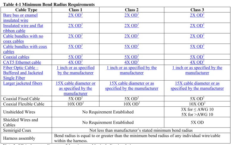
4.5.2 Routing – Bend Radius
Bend radius is measured along the inside curve of the wire or wire bundles. Table 4-1 Minimum Bend Radius Requirements
Cable Type Class 1 Class 2 Class 3
Bare bus or enamel
insulated wire 2X OD
1 2X OD1 2X OD1
Insulated wire and flat
ribbon cable 2X OD
1 2X OD1 2X OD1
Cable bundles with no coax cables
2X OD1 2X OD1 2X OD1
Cable bundles with coax
cables 5X OD
1 5X OD1 5X OD1
Coaxial cables 5X OD1 5X OD1 5X OD1
CAT5 Ethernet cable 4X OD1 4X OD1 4X OD1
Fiber Optic Cable – Buffered and Jacketed Single Fiber
1 inch or as specified
by the manufacturer 1 inch or as specified by the manufacturer 1 inch or as specified by the manufacturer Larger jacketed fibers 15X cable diameter or
as specified by the manufacturer
15X cable diameter or as specified by the manufacturer
15X cable diameter or as specified by the manufacturer
Coaxial Fixed Cable 5X OD1 5X OD1 5X OD1
Coaxial Flexible Cable 10X OD1 10X OD1 10X OD1
Unshielded Wires No Requirement Established 3X for 5X for >AWG 10 ≤ AWG 10
Shielded Wires and
Cables No Requirement Established 5X OD
Semirigid Coax Not less than manufacturer’s stated minimum bend radius
Harness assembly Bend radius is equal to or greater than the minimum bend radius of any individual wire/cable within the harness. Note 1: OD is the outer diameter of the wire or cable, including insulation.
Note 2: Coaxial Fixed Cable - Coaxial cable that is secured to prevent movement; not expected to have the cable repeatedly flexed during operation of the equipment.
Note 3: Coaxial Flexible Cable - Coaxial cable that is or may be flexed during operation of the equipment. Acceptable – Class 1, 2, 3
• Minimum bend radius meets requirements of Table 4-1. Defect – Class 1, 2, 3
• Bend radius is less than the minimum bend radius requirements of Table 4-1.
Changes from Revision D to Revision E; references in the figure boxes refer to the source picture or indicate if a new picture is being used. Clause number changes as a result of reorganizing within this chapter are not shown.
4.5.3 Routing – Coaxial Cable
Acceptable - Class 1, 2, 3
• Inside bend radius meets the criteria of Table 4-1. Defect - Class 1, 2, 3
• Inside bend radius does not meet the criteria of Table 4-1. Defect - Class 3
• Tie wraps/straps that cause any deformation of coaxial cables.
4.5.4 Routing – Unused Wire Termination
Target - Class 1, 2, 3
• Sleeving extends three wire diameters past end of wire.
• Unused wire is folded back and tied into the wire bundle. Acceptable - Class 1, 2, 3
• Ends of unused wires are covered with shrink sleeving.
• Wire may extend straight down length of bundle (Figure 4-59) or be folded back (Figure 4-60).
• Sleeving extends at least 2 wire diameters beyond end of wire.
• Sleeving extends onto the wire insulation for a minimum of 4 wire diameters or 6 mm [0.24 in], whichever is greater.
• Unused wire is tied into the wire bundle. Process Indicator - Class 2
Defect - Class 3
• Insulating sleeving extends beyond end of wire less than two wire diameters.
• Insulating sleeving extends onto wire insulation less than 4 wire diameters or 6 mm [0.24 in], whichever is greater. Defect - Class 1, 2, 3
• Ends of unused wires are exposed.
• Unused wire is not tied into the wire bundle. Figure 4-54 610D-04-049
Figure 4-55 610D-04-050
Figure 4-56 610D-04-052
Figure 4-57 610D-04-051
4.5.5 Routing – Ties over Splices and Ferrules
Acceptable - Class 1, 2, 3
• Tie wraps/straps are placed near splices or solder ferrules contained in the wire bundle.
• No stress on wires exiting splices. Acceptable - Class 1
Process Indicator – Class 2 Defect – Class 3
• Tie wraps/straps are placed over splices or solder ferrules contained in the wire bundle.
Defect-Class 1, 2, 3
• Tie wrap/strap is placing stress on the wire(s) exiting the splice.
Figure 4-59 610D-04-054
Figure 4-60 610D-04-055
Changes from Revision D to Revision E; references in the figure boxes refer to the source picture or indicate if a new picture is being used. Clause number changes as a result of reorganizing within this chapter are not shown.
©Copyright 2010. IPC, Bannockburn, Illinois. All rights reserved under both international and Pan-American copyright conventions. Any copying, scanning or other reproduction of these materials without the prior written consent of the copyright holder is strictly prohibited and constitutes infringement under the Copyright Law of the United States.
5 Soldering
This section establishes the acceptability requirements for soldered connections of all types, e.g., SMT, terminals, through-hole, etc. Although Class 1, 2 and 3 applications and environments have been considered, the nature of the soldering process may dictate that an acceptable connection will have the same characteristics for all three classes, and an unacceptable connection would be rejected for all three classes.
Where appropriate, the type of soldering process used has been addressed specifically in the criteria description. In any case, the connection criteria apply regardless of which methods of soldering have been utilized, for example:
• Soldering irons.
• Resistance soldering apparatus. • Induction wave, or drag soldering. • Reflow soldering.
• Intrusive soldering.
As an exception to the above, there are specialized soldering finishes, (e.g., immersion tin, palladium, gold, etc.) that require the creation of special acceptance criteria other than as stated in this document. The criteria should be based on design, process capability and performance requirements.
Wetting cannot always be judged by surface appearance. The wide range of solder alloys in use may exhibit from low or near zero degree contact angles to nearly 90 º contact angles as typical. The acceptable solder connection mustshall indicate evidence of wetting and adherence where the solder blends to the soldered surface.
The solder connection wetting angle (solder to component and solder to PCB termination) isshall not exceed 90º (Figure 5-1 A, B). As an exception, the solder connection to a termination may exhibit a wetting angle exceeding 90 º (Figure 5-1 C, D) when it is created by the solder contour extending over the edge of the solderable termination area or solder resist.
<following moved down to 5.1 and modified>The primary difference between the solder connections created with processes using tin-lead alloys and processes using lead free alloys is related to the visual appearance of the solder. This standard provides visual criteria for inspection of both tin-lead and lead-free connections. Figures specific to lead-free connections will be identified with the symbol:
Acceptable lead-free and tin-lead connections may exhibit similar appearances but lead free alloys are more likely to have: •Surface roughness (grainy or dull).
•Greater wetting contact angles.
All other solder fillet criteria are the same.
Typical tin-lead connections have from a shiny to a satin luster, generally smooth appearance and exhibit wetting as exemplified by a concave meniscus between the objects being soldered. High temperature solders may have a dull
appearance. Touch-up (rework) of soldered connections is performed with discretion to avoid causing additional problems, and to produce results that exhibit the acceptability criteria of the applicable class.
The following topics are addressed in this section:
5.2.5 Cold/Rosin Connection 5.2.6 Dewetting
5.2.7 Excess Solder
5.2.7.1 Excess Solder- Solder Balls/Solder Fines 5.2.7.2 Excess Solder- Bridging
5.2.7.3 Excess Solder- Solder Webbing/Splashes 5.2.8 Disturbed Solder
5.2.9 Fractured Solder 5.2.10 Solder Projections 5.2.11 Lead Free Fillet Lift
5.2.12 Lead Free Hot Tear/Shrink Hole
5.2.13 Probe Marks and Other Similar Surface Conditions in Solder Joints
5.1 Soldering Acceptability Requirements
See 5.2 for examples of soldering anomalies.
Target – Class 1, 2, 3
• Solder fillet appears generally smooth and exhibits good wetting of the solder to the parts being joined. • Outline of the parts is easily determined.
• Solder at the lead being joined creates a feathered edge.
• Fillet is concave in shape.
Acceptable - Class 1, 2, 3
• There are materials and processes, e.g. lead free alloys and slow cooling with large mass PCBs, that may produce dull matte, gray, or grainy appearing solders that are normal for the material or process involved. These solder connections are acceptable. • The solder connection wetting angle (solder to
component and solder to PCB termination) do not exceed 90º (Figure 5-1 A, B).
- As an exception, the solder connection to a termination may exhibit a wetting angle exceeding 90 º (Figure 5-1 C, D) when it is created by the solder contour extending over the edge of the solderable termination area or solder resist.
The primary difference between the solder connections created with processes using tin-lead alloys and processes using lead free alloys is related to the visual appearance of the solder. This standard provides visual criteria for inspection of both
Changes from Revision D to Revision E; references in the figure boxes refer to the source picture or indicate if a new picture is being used.
All other sSolder fillet criteria for SnPb and lead-free alloys are the same.
Typical tin-lead connections have from a shiny to a satin luster, generally smooth appearance and exhibit wetting as exemplified by a concave meniscus between the objects being soldered. High temperature solders may have a dull
appearance. Touch-up (rework) of soldered connections is performed with discretion to avoid causing additional problems, and to produce results that exhibit the acceptability criteria of the applicable class.
Figures 5-4 through 5-25 illustrate acceptable solder connections with various solder alloys and process conditions.<These figures were removed from this chapter but are displayed in appropriate places throughout Revision E>
5.2 Soldering Anomalies
5.2.1 Soldering Anomalies - Exposed Basis Metal
Exposed basis metal on component leads, conductors or land surfaces from nicks, scratches, or other conditions cannot exceed the requirements of 7.1.2.3 for leads and 10.2.9.1 for conductors and lands.<redundant to bullets below>
Component leads, sides of land patterns, conductors, and use of liquid photoimageable solder resist can have exposed basis metal per original designs.
Some printed circuit board and conductor finishes have different wetting characteristics and may exhibit solder wetting only to specific areas. Exposed basis metal or surface finishes should be considered normal under these circumstances, provided the achieved wetting characteristics of the solder connection areas are acceptable.
Acceptable - Class 1, 2, 3 • Exposed basis metal on:
- Vertical conductor edges.
- Cut ends of component leads or wires.
- Organic Solderability Preservative (OSP) coated lands.
• Exposed surface finishes that are not part of the required solder fillet area.
Acceptable - Class 1
Process Indicator - Class 2, 3
• Exposed basis metal on component leads, conductors or land surfaces from nicks or scratches provided conditions do not exceed the requirements of 7.1.2.3 for leads and 10.3.1 for conductors and lands.
Defect – Class 1, 2, 3
• Exposed basis metal on component leads, conductors, or land surfaces from nicks, scratches, or other conditions exceed the requirements of 7.1.2.3 and 10.3.1.
Figure 5-4 610D-05-026 Figure 5-5 610D-05-027
Figure 5-6 610D-05-028 Figure 5-7 610D-05-009
5.2.2 Soldering Anomalies - Pin Holes/Blow Holes
Acceptable - Class 1
Process Indicator - Class 2, 3
• Blowholes (Figures 5-8, 9), pinholes (Figure 5-10), voids (Figures 5-11, 12), etc., providing the solder connection meets all other requirements.
Defect – Class 1, 2, 3
• Solder connections where pin holes, blow holes, voids, etc. reduce the connections below minimum requirements (not shown).
5.2.3 Soldering Anomalies - Reflow of Solder Paste
Defect - Class 1, 2, 3
• Incomplete reflow of solder paste.
5.2.4 Soldering Anomalies - Nonwetting
IPC-T-50 defines nonwetting as the inability of molten solder to form a metallic bond with the basis metal. In this Standard, that includes surface finishes, see 5.2.1.
Defect - Class 1, 2, 3
• Solder has not wetted to the land or termination where solder is required. (Figures 5-17, 18, 19 component terminations, Figure 5-20 shield termination, Figure 5-21 wire termination)
• Solder coverage does not meet requirements for the
Figure 5-8 new
Figure 5-9 610D-05-030 Figure 5-10 610D-05-031 Figure 5-11 610D-05-032 Figure 5-12 610D-05-033
Figure 5-13 610D-05-034 Figure 5-14 610D-05-035 Figure 5-15 new
Figure 5-16 new
Figure 5-17 new Figure 5-18 new Figure 5-19 new
Changes from Revision D to Revision E; references in the figure boxes refer to the source picture or indicate if a new picture is being used.
5.2.5 Soldering Anomalies – Cold/Rosin Connection
IPC-T-50 defines cold solder connection as “A solder connection that exhibits poor wetting, and that is characterized by a grayish, porous appearance. (This is due to excessive impurities in the solder, inadequate cleaning prior to soldering, and/or the insufficient application of heat during the soldering process.)” A rosin solder connection is defined in IPC-T-50 as “A solder connection that has practically the same appearance as does a cold solder connection, but that also shows evidence of entrapped rosin separating the surfaces to be joined.”
Defect - Class 1, 2, 3
• Nonwetting or incomplete wetting as a result of a cold (Figure 5-22) or rosin (not shown)
connection.
5.2.65.2.5 Soldering Anomalies - Dewetting
IPC-T-50 defines dewetting as a condition that results when molten solder coats a surface and then recedes to leave
irregularly-shaped mounds of solder that are separated by areas that are covered with a thin film of solder and with the basis metal or surface finish not exposed.
Defect - Class 1, 2, 3
• Evidence of dewetting that causes the solder connection to not meet the SMT or thru-hole solder fillet requirements.
5.2.75.2.6 Soldering Anomalies - Excess Solder
Metal lidded components
Solder splashes or tinning on a metalized package body (see Figure 5-27) should be evaluated for impact upon hermetic and radiation hardening performance of the component considering the intended performance environment. Solder splashes on the metalized surfaces may be acceptable if the extended electrical performance is not required or compromised.
Figure 5-22 New
Figure 5-23 610D-05-041 Figure 5-24 610D-05-042 Figure 5-25 610D-05-043 Figure 5-26 610D 6-105
5.2.7.15.2.6.1 Soldering Anomalies - Excess Solder- Solder Balls/Solder Fines
Solder balls are spheres of solder that remain after the soldering process. Solder fines are typically small balls of the original solder paste metal screen size that have splattered around the connection during the reflow process.
Target – Class 1, 2, 3
• No evidence of solder balls on the printed wiring assembly.
Acceptable – Class 1, 2, 3
•Solder balls are entrapped/encapsulated and do not violate minimum electrical clearance.
• Solder balls are entrapped, encapsulated or attached (e.g. in no-clean residue, with conformal coating, soldered to a metal surface, embedded in the solder resist or under a component).
• Solder balls do not violate minimum electrical clearance.
Note: Entrapped/encapsulated/attached is intended to mean that normal service environment of the product will not cause a solder ball to become dislodged.
Defect - Class 1, 2, 3
• Solder balls are not entrapped, encapsulated or attached or can become dislodged in the normal service environment.
• Solder balls violate minimum electrical clearance. • Solder balls are not entrapped in no-clean residue or
encapsulated with conformal coating, or not attached (soldered) to a metal surface, Figures 29 through 5-32.
5.2.7.25.2.6.2 Soldering Anomalies - Excess Solder- Bridging
Defect - Class 1, 2, 3
• A solder connection across conductors that should
Figure 5-28 610D-05-044
Figure 5-29 new
Figure 5-30 610D-05-046 Figure 5-31 610D-05-047 Figure 5-32 610D-05-048 Figure 5-33 new
Changes from Revision D to Revision E; references in the figure boxes refer to the source picture or indicate if a new picture is being used.
5.2.7.35.2.6.3 Soldering Anomalies - Excess Solder- Solder Webbing/Splashes
Inspection for solder splashes shall be done without magnification.
Target – Class 1, 2, 3
• No solder splashes or webbing.
Acceptable – Class 1, 2, 3
• Solder splashes or metallic particles meet the following criteria:
• Attached/entrapped/encapsulated on the PCA surface or solder mask, or soldered to metallic surface.
• Do not violate minimum electrical clearance.
Defect - Class 1, 2, 3
• Solder splashes/webbing.
• Solder splashes that are not attached, entrapped, encapsulated.
• Solder splashes on metal component surfaces impact form, fit or function, e.g. damages lid seal on hermetic components.
• Violate minimum electrical clearance.
Note: Entrapped/encapsulated/attached is intended to mean that normal service environment of the product will not cause solder to become dislodged.
5.2.85.2.7 Soldering Anomalies - Disturbed Solder
Surface appearance with cooling lines as shown in Acceptable Figures 5-40 (lead free) and 5-41 (SnPb) are more likely to occur in lead free alloys and are not a disturbed solder condition.
Acceptable - Class 1, 2, 3
• Lead free and tin-lead solder connections exhibit: • cooling lines (Figures 5-40, ).
• Secondary reflow (Figure 5-41)
Defect - Class 1, 2, 3
•Disturbed solder joint characterized by stress lines from movement in the connection.
• Disturbed solder joint characterized by uneven surface from movement in the solder connection during cooling.
Figure 5-38 610D-05-054 Figure 5-39 610D-05-055
Figure 5-40 610D-05-056 Figure 5-41 610D-5-58
Figure 5-42 610D-05-057 Figure 5-43 610D-05-059
5.2.95.2.8 Soldering Anomalies - Fractured Solder
Defect - Class 1, 2, 3
• Fractured or cracked solder.
5.2.105.2.9 Soldering Anomalies - Solder Projections
Defect - Class 1, 2, 3
• Solder projection, Figure 5-47, violates assembly maximum height requirements or lead protrusion requirements.
• Projection, Figure 5-48 violates minimum electrical clearance (1).
5.2.115.2.10 Soldering Anomalies – Lead Free Fillet Lift
These criteria are applicable to plated-through hole connections.
Acceptable – Class 1, 2, 3
• Fillet lifting - separation of the bottom of the solder and the top of the land. The connection with the lifted fillet must meet all other acceptance criteria.one the primary side of plated-through hole connection). Note: (From IPC-T-50H) Fillet lifting is the phenomenon in which the solder fillet is lifted off from the land on a board mainly during the flow solder process. The phenomenon is more likely to occur on the primary (solder destination) side rather than on the secondary (solder source) side which is exposed to flow soldering. Figure 5-51 is a microsection view of fillet lifting. There is no defect associated with this anomaly. Note: See 10.3.2 for criteria related to land damage that may be caused by fillet lifting.
Figure 5-44 610D-05-061 Figure 5-45 610D-05-062 Figure 5-46 new
Figure 5-47 610D-05-063 Figure 5-48 610D-05-064 Figure 5-49 610D-05-065
Figure 5-50 610D-05-066 Figure 5-51 new
Changes from Revision D to Revision E; references in the figure boxes refer to the source picture or indicate if a new picture is being used.
5.2.125.2.11 Soldering Anomalies – Lead Free Hot Tear/Shrink Hole
There is no defect associated with this anomaly provided the connection meets all other acceptance criteria. Figures 5-52 and 5-53 are examples of hot tear.
Acceptable – Class 1, 2, 3
•For connections made with lead free alloys: •The bottom of the tear is visible.
•The tear or shrink hole does not contact the lead, land or barrel wall.
Defect – Class 1, 2, 3
•Shrink holes or hot tear in connections made with SnPb solder alloys.
•For connections made with lead free alloys: •The bottom of the shrink hole or hot tear is not
visible.
•The tear or shrink hole contacts the lead or land.
5.2.135.2.12 Probe Marks and Other Similar Surface Conditions in Solder Joints
Target – Class 1, 2, 3
• The solder joint is free of any probe marks and other similar surface conditions.
Acceptable – Class 1, 2, 3
• Probe marks and other similar surface conditions that do not violate other requirements.
Defect – Class 1, 2, 3
• Probe marks and other similar surface conditions cause damage in excess of requirements.
Figure 5-52 610D-05-067 Figure 5-53 new
Figure 5-54 new
copying, scanning or other reproduction of these materials without the prior written consent of the copyright holder is strictly prohibited and constitutes infringement under the Copyright Law of the United States.
6 Terminal Connections
These criteria apply to both wires and component leads. The target wrap conditions achieve a mechanical connection between the lead/wire and the terminal sufficient to assure that the lead/wire does not move during the soldering operation. Typically the mechanical connection includes a 180 º mechanical wrap to effect mechanical connection.
As an exception to the wrap conditions described above, it is acceptable when attaching leads/wires to bifurcated, slotted, pierce, punched or perforated terminals for the lead/wire to extend straight through the opening of the terminal with no wrap. Except for slotted terminals (6.10) leads/wires with no wrap need to be staked, bonded, or constrained to a degree that the attachment is mechanically supported, see 6.9.1 and 6.9.3. The purpose is to prevent transmission of shock, vibration, and movement of the attached wires that could degrade the solder connection.
The criteria in this section are grouped together in sixteen main subsections. Not all combinations of wire/lead types and terminal types can possibly be covered explicitly, so criteria is typically stated in general terms to apply to all similar combinations. For example, a resistor lead and a multistranded jumper wire connected to turret terminals have the same wrap and placement requirements, but only the multistranded wire could be subject to birdcaging.
In addition to the criteria in this section the criteria of Section 5 are applicable., solder connections must meet the criteria of Section 5.
The following topics are addressed in this section: 6.1 Swaged Hardware
6.1.1 Terminals
6.1.1.1 Terminal Base – Pad Gap 6.1.1.2 Terminals - Turret 6.1.1.3 Terminals - Bifurcated 6.1.2 Rolled Flange
6.1.3 Flared Flange 6.1.4 Controlled Split 6.1.5 Solder
6.2 Insulation
6.2.1 Damage 6.2.2.1 Presolder 6.2.2.2 Post-Solder 6.2.3 Clearance 6.2.4 Flexible Sleeve 6.2.4.1 Placement 6.2.4.2 Damage
6.3 Conductor
6.3.1 Deformation
6.3.2 Conductor – Strand Damage