Journal of Chemical and Pharmaceutical Research, 2014, 6(2):77-82
Research Article
CODEN(USA) : JCPRC5
ISSN : 0975-7384
Design of experiments of electromigration reliability for solder joints of a
wafer level chip scale package
Yuanxiang Zhang
*and Yingyu Ji
College of Mechanical Engineering, Quzhou University, Quzhou, China
_____________________________________________________________________________________________
ABSTRACT
Electromigration (EM) in solder joints under high current density has become a critical reliability issue for the future high density microelectronic packaging. This paper presents a prediction method for electromigration (EM) induced void generation of solder joint in a wafer level Chip Scale Package (WL-CSP) structure. The driving force for electromigration induced failure considered here includes the electron wind force, stress gradients, temperature gradients, as well as the atomic density gradient. To understand impact of the under ball metallurgy (UBM) geometry and solder bump shape on electromigration reliability, the EM simulation for WL-CSP structure is performed to get time to failure (TTF) based on the full factorial design of experiments (DOE) by using 3D finite element analysis. The analysis of the impact of under ball metallurgy and solder bump geometry on the void generation and TTF is presented.
Key words: Electromigration; time to failure; solder joint; void prediction
_____________________________________________________________________________________________
INTRODUCTION
It is well known that, as the electronics industry continues to push for high performance and miniaturization, the demands of higher current densities increases. This may cause electromigration failures, not only in integrated circuit (IC) interconnects but also in solder joints of IC packages. [1].The solder bump under a flip CSP or a WL-CSP has a UBM on the chip side and a bump pad on substrate side. One challenge we face as the chip size shrinks, is how to design a robust UBM and solder bump shape to reduce the electromigration failure and to obtain the longer time to failure (TTF) life in a optimization solution.
In a solder system of a flip chip or a CSP, the failure phenomenon of electromigration has been found inside the solder joint which is adjacent to the under bump metallization (UBM) layer [2]. Due to the unique geometry of a flip chip, current crowding occurs at the contact interface between the solder bump and the UBM. The current crowding and the high temperature at the contact interface between the solder bump and the UBM causes the formation of voids [3]. The void propagates across the entire solder/UBM interface and leads to failure finally. Therefore, how to design the UBM geometry with different UBM rim angles to improve the failure life of EM is essential. In order to make the failure life of the package structure as longer as possible, some studies tried to optimize the ball shapes at ball level, such as the double-bump [4]. It also indicated that the double-bump WLP had much better reliability than standard WLP packages under thermal cycling. But whether it has a better EM life needs to be studied further.
BASIC ELECTROMIGRATION FORMULATION
Electromigration is a diffusion process which is controlled by masstransportation. The time dependent evolution equation of the local atomic density can be given as
0 = ∂ ∂ + ⋅ ∇ t c q (1)
Where c is the normalized atomic density (NAD), c=C/C0, C is the actual atomic density and C0 is the initial
(equilibrium state) atomic density in the absence of a stress field, t is the time; q is the total normalized atomic flux.
The atomic density includes electron windforce, stress gradients, temperature gradients, and the atomic densitygradient, respectively. The total normalized atomic flux can be written by [5]
(
T)
D cc c D kT cD T T Q kT cD e Z kT cD m m C S Th
Ew + Ω∇ − ∇ = ⋅ − ∇
∇ − = + + + = * * , , , j F j q q q q
q ρ σ σ (2)
where
(
m)
mkT D T T Q kT D e Z kT D
T σ = * ρ − *∇ + Ω∇σ
, ,
, j j
F (3)
where k is Boltzmann’s constant; e is the electronic charge; *
Z is the effective charge which is determined
experimentally; T is the absolute temperature;ρis the resistivity which is calculated as ρ=ρ0
(
1+α(
T−T0)
)
, whereαis the temperature coefficient of the metallic material, ρ0is the resistivity at T0; j is the current density vector; *
Q is the heat of transport; Ωis the atomic volume; σm =
(
σ1+σ2+σ3)
/3 is the local hydrostatic stress, where σ1,σ2, σ3 are the components of principal stress; D is the effective atom diffusivity, − = kT E D D a exp
0 , where Ea is the
activation energy, D0 is the effective thermally activated diffusion coefficient.
For the EM evolution equation (Eq. (1))on any enclosed domain V with the corresponding boundaryΓ, the atomic flux boundary conditions (B.C.) of metal interconnects can usually be expressed as
Γ =
⋅n q0 on
q (4)
For blocking boundary condition,
Γ
=0 on
q0 (5)
For the initial time, the normalized atomic density for all nodes is
1
0 =
c (6)
The above equations and boundary conditions constitute the boundary value problem that governs the atomic transport during EM. This boundary value problem must be solved accurately in order to adequately describe the continuous atom redistribution and to capture the realistic kinetics of void nucleation and growth as a function of the interconnect architecture, segment geometry, material properties, and stress conditions. Different from previous methodology, the effect of atomic density gradient is not neglected; it is included in equation (1).
Assume that there is a critical normalized atomic density for void initiation, * min
c , and for hillock initiation, * max
c .
When the normalized atomic density c is less than or equal to * min
c ( * min
c
c≤ ), a void will appear [7]. Conversely,
when the normalized atomic density c is greater than or equal to * max
c ( * max
c
c≥ ), a hillock will be generated. For the
solder material, a criterion for void generation is selected to be * min
c =0.85. The work in this paper can show the location of hillock, but it has not yet considered the formation of a hillock. In the simulation procedure of the void growth period, once the average atomic density value of the elements are less than the critical atomic density for void initiation *
min
c , the corresponding elements will be killed ("element death") and the structure need to be reconstructed. To achieve the "element death" effect, ANSYS do not actually remove "killed" elements. Instead, it deactivates them by reducing the element material attribute, such as the elastic modulus and resistivity, by a factor of1.0E-6.In the semiconductor industry for a WL-CSP bump failure criterion, a 15% increment in electrical resistance of the bump is usually considered EM failure. This criterion is used in this work to get the final TTF.
EM FAILURE ANALYSIS FOR SOLDER JOINTS IN WL-CSP
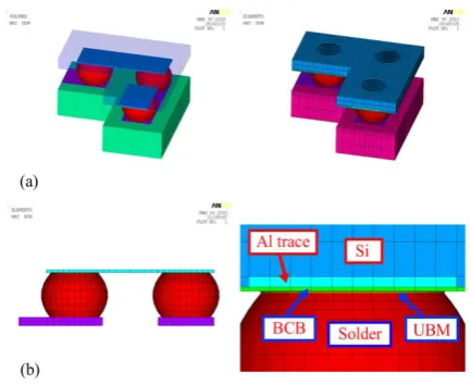
Gee et al. [3] have done the electromigration test for SnAgCu and SnPb solder joints in a WL-CSP package. The package has 36 solder bumps with 500 µm pitch. The dimension of silicon chip is 1.6 mm×1.6mm×0.5mm. Solder bumps are 0.15 mm in diameter and 0.2 in height. The exterior 20 solder bumps are assumed to connect with each other in a daisy chain as shown in Fig.1. Sub-model technique in ANSYS is introduced to get the better response of the electronic migration. The global thermal-electric coupled field model uses Solid69 element and the global stress model uses Visco107 element for solder bumps and Solid45 element for the remaining parts of the model. Firstly, the global structure is modeled using relative coarse elements firstly. Secondly, a refined thermal-electric coupled field sub-model and a refined stress sub-model with UBM (Al/NI(V)/Cu) layer are then constructed as shown in Fig. 2.
[image:3.595.197.414.478.655.2]Fig. 1: WL-CSP package model: (a) WL-CSP package structure; (b) local view
Fig. 2: Sub-model of WL-CSP structure: (a) solid sub-model and its mesh; (b) local view of solder bump
The solder bump material is 95SnAg4.5Cu0.5. The related thermal mechanical and electrical constants used in the simulation are taken from refs. [6, 8].The electromigration parameters of solder bumps are selected from the previous refs [8-10, 18]. In addition, for the solder bump EM void failure, * 0.85
min =
c and * 1.15
max =
Fig. 3: Electron flow direction in a global model
[image:4.595.232.383.532.642.2]Fig. 4: Temperature and current density distribution of solder bump
Fig. 5: Void formation between simulation solutions and test results
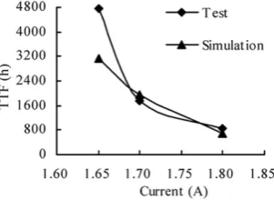
Fig. 6:Comparison of TTF between simulation solutions and test results
that the simulated TTF data agree well with the tested mean time to failure (MTTF). There is some difference in the current of 1.65A, this might be either due to the modeling setting up and selected parameters need to be further validated or the error of the test system.
PARAMETER SIMULATIONS FOR UBM AND SOLDER BUMP
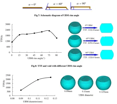
The parameters of DOE include UBM rim angle, UBM diameter, and UBM thickness and solder bump shape. Fig.7 gives the schematic three different UBM rim angles. Table 1 lists the total parameters of DOE. The current 1.7A is applied in this section.
Table 1: Design parameters of DOE
Design parameters Value
UBM rim angle 0º, 15º, 30º, 45º, 60º, 75º, 90º
UBMdiameter 0.09mm, 0.11mm, 0.125mm
UBMthickness 0.00106mm, 0.00212mm, 0.00424mm
Solder bump shape Ball, Cylinder, Square Cube, Double ball
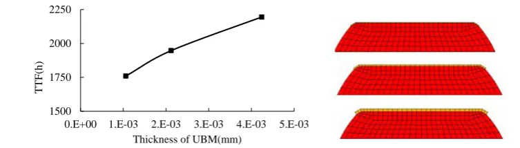
[image:5.595.114.510.342.694.2]Fig.8show the TTF and voidwith different UBM rim angle. It shows that the UBM geometry has a significant impact on the solder bump void growth and TTF. The 75°UBM rim angle get the longest the solder bump TTF, the 0°UBM and the 90°UBM rim angle is the poor structures to withstand the electromigration failure. Fig.8 alsoshows voids with three UBM rim angles. It is obsevered that all these voids appear in the solder bump adjacent to the UBM layer.Fig.9 shows the impact of UBM diameter on TTF. As the UBM diameter increases, the EM life also increases. Fig. 10 shows the impact of UBM thickness on TTF with 30° UBM rim angle. From Fig. 10, it can be observed that the thicker of UBM, the longer of the TTF life.
Fig.7: Schematic diagram of UBM rim angle
Fig.8: TTF and void with different UBM rim angle
Fig.9: TTF and void with different UBM diameter 0
600 1200 1800 2400 3000
0 15 30 45 60 75 90
TTF
(h
)
UBM rim angle(°)
0 500 1000 1500 2000 2500
0.08 0.09 0.1 0.11 0.12 0.13
TTF
(h
)
UBM diameter(mm)
° =0
Fig.10: TTF with different UBM thicknesses
In order to study the impact of shapes of ball on EM TTF life, this paper selects cylinder, cube and single and dual balls. Those shapes keep the same volume with the same height (except dual ball). The dual ball has twice the volume of a single ball. Table 2 gives the TTF comparison with different bump shapes. From the Table 2 it can be seen that the cylinder bump has the longest TTF while dual bump gives the shortest TTF.
Table 2: TTF of different Solder bump shapes
Solder bump shapes TTF(hours)
Spheroid 1947.2
Cylinder 20458.6
Cube 15941.7
Double ball 945.3
CONCLUSION
The simulation results show that the UBM geometry and bump shape have significant impact on the solder bump void growth and TTF. There is a best solution for UBM rim angle (750 in the bump layout of this paper). A thicker and larger diameter UBM will help to produce the longer bump TTF. Simulation also shows that if we keep the same shape of solder bump, the larger (and higher) the solder bump, the longer the TTF. In addition to that, different bump shapes in dual ball, ball, cylinder and cube are studied. The results show that the cylinder bump gives the longest TTF life following by the cube bump and the single ball bump, while the double ball bump is found to have the shortest TTF. It is the weakest bump to withstand the electromigration failure. Therefore in WL-CSP design, a robust design against electromigration should consider optimized UBM and bump geometry parameters to get the best solution, like selecting a thicker UBM, shorter bump pitch, lower bump and cylindrical bump shape.
Acknowledgments
This research was funded by Zhejiang Provincial Natural Science Foundation (No.LQ13E050014) and Scientific Research Project of Zhejiang Provincial Education Department (Y201225809).
REFERENCES
[1]K Croes, C J Wilson, M Lofrano, et al. Microelectronic Engineering, 2011, 88(5), 614-619.
[2]S H Chae, X Zhang, K H Lu, et al. Journal of Materials Science: Materials in Electronics, 2007, 18, 247-258. [3]S Gee, N Kelkar, J Huang, et al. Proceeding of InterPACK2005, 2005, 73417.
[4]X J Fan, Q Han. Proceeding of 10th Electronics Packaging Technology Conference, 2008, 834-841. [5]J P Jing, L H Liang, M Guang. ASME Journal of Electronic Packaging, 2010, 132(1),1-7.
[6]Y Liu, L H Liang, S Irving, et al. Microelectronics Reliability, 2008, 48(6),811-824.
[7]K Sasagawa, M Hasegawa, M Saka, et al. Journal of Applied Physics, 2002, 91(11), 9005-9014. [8]R Darveaux. ASME Journal of Electronic Packaging, 2002, 124(3), 147-152.
[9]C Basaran, M Lin. International Journal of Solids and Structures, 2007, 44(14-15), 4909-4924. [10]C Basaran, M Lin. Mechanics of Materials, 2008, 40(1-2), 66-79.
1500 1750 2000 2250
0.E+00 1.E-03 2.E-03 3.E-03 4.E-03 5.E-03
TTF
(h
)
![μ Carbonato κ4O,O′:O′,O′′ bis{[2′ (di tert butylphosphanyl)biphenyl 2 yl κ2P,C1]palladium(II)} dichloromethane monosolvate](data:image/gif;base64,R0lGODlhAQABAIAAAP///wAAACH5BAEAAAAALAAAAAABAAEAAAICRAEAOw==)