A New Zero-Voltage-Switching Push-Pull Converter
Yisheng Yuan, Qunfang Wu
School of Electrical and Electronics Engineering, East China Jiaotong University, Nanchang, China Email: [email protected], [email protected]
Received March, 2013
ABSTRACT
A soft switching three-transistor push-pull(TTPP)converter is proposed in this paper. The 3rd transistor is inserted in the primary side of a traditional push-pull converter. Two primitive transistors can achieve zero-voltage-switching (ZVS) easily under a wide load range, the 3rd transistor can also realize zero-voltage-switching assisted by leakage inductance. The rated voltage of the 3rd transistor is half of that of the main transistors. The operation theory is explained in detail. The soft-switching realization conditions are derived. An 800 W with 83.3 kHz switching frequency prototype has been built. The experimental result is provided to verify the analysis.
Keywords: Push Pull Converter; Extra Transistor; Zero-voltage-switching
1. Introduction
The soft-switching technology can reduce device stress, switching loss, electromagnetic interference (EMI) and improve power density of the power electronic equip-ment. Over the last two decades, the most researches focus on the improved ZVS and ZVZCS phase-shifted full-bridge circuit [1-6] and their applications. But com-paratively, the research on soft switching push-pull con-verter is very seldom. Taking LLC resonant technique for example, in recent years, LLC resonant converter based on half-bridge circuit, three- level circuit, full-bridge circuit and interleaved combined circuit [7-12] attracted lots of interest, owing to its full soft-switching realization for all power transistors and rectifier diodes. But in LLC resonant converters’ family, the push-pull converter is exceptive. A push-pull converter has two transformer primary windings, which is impossible to have a LLC link inserted in the primary side. Converter in [13] shows soft switching behavior of the push-pull circuit with a LC resonant link in secondary side. But further research in [14]shows that there exists N-period resonant status in this type of the push-pull converter and its output will work as either constant voltage source or constant current source. Similarly, LCL resonant push-pull converter [15-17] where resonant components are located in either primary side or secondary side can also realize ZVS of power switches, but can not adjust its output voltage. Furthermore, the LCL resonant push-pull converter [18] with an additional parallel resonant inductor Lsrcan real-ize ZVS for power switches and can adjust its output voltage by frequency modulation. But in order to im-prove boost ratio, the additional parallel resonant
induc-tor Lsrhas to be designed so small that extra power loss is become larger. Besides the above passive soft-switching push-pull converter, Active-clamped push-pull circuitin [19] can achieve ZVS for its main power switches, but its drawbacks are that the maximum duty cycle of main power switches is limited by active-clamped circuit. The three-level push-pull circuit [20] controlled by phase- shifted PWM mode can obtain ZVS condition for power switches, but its controller UC3875 is expensive. Both these two active soft-switching push-pull converters re-quire four power switches and their driving logics is complex.
This paper proposes a three-transistor push-pull (TTPP) converter. ZVS can be achieved for all three transistors based on the proposed driving logic. The TTPP converter can be controller by a general PWM IC of SG3525.
2. Operation Principle
2.1. Converter Topology
The proposed TTPP converter is showed in Figure 1. An
extra transistor Q3 is inserted between the power source
Uin and midpoint of two primary windings. Diodes D1,
D2 and D3 are body diodes of the transistors Q1, Q2 and
Q3 respectively. Capacitors C1, C2 and C3 include the parasitic capacitor of power transistors and external par-allel capacitors. The inductance Lleak-1 and Lleak-2 represent the leakage inductances of the primary winding P1 and P2 respectively.
2.2. PWM Mode
showed in Figure 2. The duty cycle of the Q1 and Q2 are higher than 0.5, and they are 180º out of phase. The switching frequency of Q3 is twice of that of Q1 and Q2.
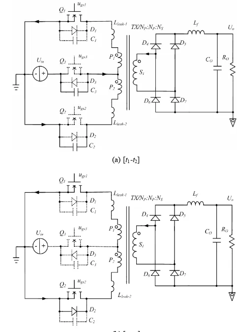
[image:2.595.76.418.217.724.2]1 and 0 represent switch on and switch off respectively. Neglecting the dead time, such as t1~t2, t3~t4, the operat-ing status of the Q1, Q2 and Q3 can be divided into four states, 101→110→011→110 in a complete cycle. To ensure voltage-second balance of the transformer in a switching cycle, the state 101 is lasts as long as the state 011.
Figure 1. The proposed converter.
Figure 2. Main operation waveforms.
The state 101 and 011 are normal energy deliver stages from the primary side to the secondary side. Conversely, during state 110, the transistor Q1 & Q2 are both con-ducted and the energy is circulating in the primary side loop.
2.3. Operation Principle
To simplify the analysis of operation stage, the following conditions are assumed.
1) The voltage drop of the power MOSFETS and DI-ODES during on state is zero.
2) C1 = C2 = C3 =Cleak. 3) Lleak-1 = Lleak-2 = Lleak.
4) The output filter inductance can be modeled as a constant current source during the dead time.
The operation process of the TTPP converter in half of cycle can be divided into six stages. The main operation waveforms are shown in Figure 2. Figure 3 shows the
equivalent circuit at different modes. 1) Mode 1 [t1-t2].
Before t1, transistor Q1 and Q3 are both conducting, the energy transfer from Uin to the transformer secondary winding and the current of the filter inductance Lf in-creases. At t1, Q3 is turned off. If the capacitor C3 is large
(a) [t1-t2]
[image:2.595.295.536.392.729.2](c) [t3-t4]
(d) [t4-t5]
(e) [t5-t6]
[image:3.595.68.273.77.719.2](f) [t6-t7]
Figure 3. Equivalent circuit at different modes.
enough, the rising time of uds3 is more than several time of falling time of ids3, Q3 can achieve zero-voltage turn-off. In this mode, the inductance Lfwill keep free-wheeling and be reflected to the primary side to resonant with capacitance C3 and C2. Because current through Lf is high enough, the voltage uds3 will rise from zero up to Uin with uds2 falling from 2Uin to zero. At the same time, the transformer primary side voltage uP reduces to zero.
Assuming that the initial current of primary side loop in this mode is equal to Ip, the loop voltage equation and junction current equation in primary side can be estab-lished as
1 3
2
3 2
1 2 3 1 2
2 2
3 3
0 0
/ /
in ds p leak
in ds p ds leak
p
ds ds
di
U u u L
dt di
U u u u L
dt
I i i
i i i
i C du dt
i C du dt
(1)
Right before t2, transformer voltage up falls to zero. Combining this end condition with equation (1), the end status of this mode can be derived with approximation as in Equation (2),
2 3 1 2 2 1
0
/ 2 / 2
5 /
ds
ds in
P P
in P
u
u U
i I
i I
t t CU I
(2)
Meanwhile, in the secondary side, in general opinion,
D5&D6 keep conducting and D4&D7 keep turn off. But in practical, because the transformer voltage fall down to zero quickly, the parasitic capacitor of the secondary side of the transformer will produce a discharge current idis which will cancel part of the current of the secondary side and reduce the current through D5&D6. So D4&D7 also conduct in order to keep the current of Lf constant. In this micro-commutation mode, the current of D4&D7 is so small that it neglected in most papers. In this paper, it is defined as micro-commutation mode.
2) Mode 2 [t2-t3].
At t2 moment, the diode D2 begins to conduct because
uds2 fall down to zero. This means that transistor Q2 can achieve zero-voltage turn-on.
In this mode, D2 and Q1 are on and current circulates in the primary side. Neglecting the voltage-drop of D2 and Q1, the circulating current in the primary side main-tain at Ip/2.
and iLfbegin dropping. This will drive the currents of
D4~D7 reducing. It can be derived as:
4 7 7 4 2 ( ) P S P S
D D Lf
S D D
O Lf Lf f N i I N
i i i
i i i
U dt
i i t
L (3)
As a result, iD4 may fall down to zero. 3) Mode 3 [t3-t4]
At t3, Q1 is turned off. Q1 can achieve zero voltage turn off due to C1. The current i1 flows through Q1 decreasing rapidly, causing the secondary rectifier begin commutat-ing. The current iD5&iD6 decreases quickly and synchro-nously, iD4&iD7 increase quickly. In the primary side, the leakage inductances of Lleak-1&Lleak-2 resonate with the capacitances of C1&C3. The voltage u ds1 increases while
uds3 falls down at the same time. The secondary current reflects the change of primary resonance current.
In this mode, the following equations can be derived,
3 1 2 1 1 3 3 1 3 1 2 3 ds ds
in ds leak ds
in ds leak
i i i
du i C dt du i C dt di
U u L u
dt di
U u L
dt (4)
when the energy of leakage inductance is large enough,
uds1 increases from zero to Uin, uds3 decreases from Uin to zero , i1 drops to zero, i2 drops to equal i3, and D3 starts to conduct. As a result, it provides the Q3 ZVS condition.
The time required for voltage uds3 dropping to zero or voltage uds1 to rise from zero to Uin can be simplified as
34 1 3
2 ( ) / 2
in
CU t
i t
(5)
4) mode 4 [t4-t5]
At t4, the voltage uds3 is zero, Q3 is turned on and zero- voltage turn-on is achieved. In this interval, the voltage
Uin applies on the leakage inductance Lleak-2. The current
i2 and i3 can be expressed as,
2 3 ( )4 in leak
U dt
i i i t
L
(6)
with the change of i2 and i3, the secondary rectifier con-tinues commutating. The current iD5&iD6 decreases quickly and synchronously, iD4&iD7 increase quickly. At
the end of this stage, the currents iD5&iD6 reach their peak reverse recovery current, accordingly the current i2&i3 change from negative across zero, until its value reflected to the secondary side reach the sum of iD4 and peak re-verse recovery current iD5.
5) Mode 5 [t5-t6]
At t4, diode D5&D6 begin sustain reverse voltage quickly, leading the voltage of secondary winding begins be reverse quickly. As a result, the voltage of primary windings P1 is also reversed with the secondary voltage. The magnetizing inductance Lm resonants with C1. Volt-age uds1 rises from Uin to 2Uin, up rises from zero to Uin.
In this mode, with the decreasing of reverse recovery current of D5&D6 , the current is, i2 and i3 also decrease synchronously. This mode finishes when iD5&iD6 recov-ery to zero and up arrives Uin.
6) Mode 6[t6-t7]
In this mode, the converter run in a normal operation status and energy is transferred from input to output. The current of Lf increases linearly and the value can be ex-pressed as follows,
5
/
( ) in s p o
Lf Lf
f
U N N U dt
i i t
L
(7)
At t7, Q3 is turned off; the converter begins the next half of cycle.
3. Design Guidelines
3.1. Duty Cycle Loss
According to the above analysis, the duty cycle α3 of extra transistor Q3 determines the ratio between Uo and
Uin. But during t5 to t6, there is a duty cycle loss αloss. It is derived approximately as,
56 3( )6 loss
s leak s
t i t
T L T
(8)
where Tsrepresents the switching period of Q3. Then
3 ( ) O loss in P U
U N
S
N
2
(9)
3.2. Voltage Stress of Power Switches
The voltage stress of main transistors Q1&Q2 is 2Uin, while that of the extra transistor Q3 is Uin.
3.3. Soft-switching Condition
A) Main transistors Q1&Q2
The ZVS condition of Q1 and Q2 is determined by Lf energy. In mode 1, uds3 should rise from zero to Uin and
uds2 should fall from 2Uin to zero. So the condition of main transistor realizing soft-switching can be derived as
2 5 f Lf in
According to (14), the minimum load for obtain ZVS of Q1 and Q2 can be derived, as well as the minimum dead time t1~t2.
In addition, the turn-off loss of main transistor Q1&Q2 are far less than that in the traditional push-pull converter. In the traditional push-pull converter, the power switches are turned off at the peak current with a big turn-off losses. However, Q1&Q2 in this TTPP converter are turned off at half of peak current as that of traditional push-pull converter. Furthermore, the parallel capacitor of Q1&Q2 can reduce turn-off losses greatly.
B) Extra transistor Q3
The ZVS condition of the extra transistor Q3 is deter-mined by the energy of leakage inductance. It can be expressed as,
2 3
( ) 2 2
Leak in
L i t CU (11) Obviously, the ZVS of Q3 couldn’t be obtained easily under a light load or with small leakage inductance. In fact, adding a series inductance will be a recommended method to improve ZVS condition of Q3.
4. Experimental Results
The performance of the TTPP converter has been veri-fied with a prototype circuit operating at 83.3 kHz, 140 V~150 V input voltage, 180V output voltage and 800W power. The transformer is implemented with an EE42 core and windings with turn ratio of 24:24:42. Power MOSFETs of SPW20N60C3 and diodes of RHRP1560 are used in the prototype.
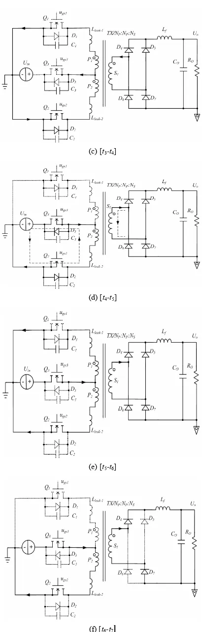
The tested gate signals of three power transistors and the secondary voltage of the transformer are shown in
Figure 4. The logics relation of three driving signals is
same as Figure 2. The secondary voltage is a three-level
waveform.
Figure 5 shows the measured waveforms of the
pro-posed converter at full load. It is obvious that Q1 achieves zero-voltage turn-on and turn off at half of peak current as shown in Figure 5(a). The extra Q3 also obtain zero-voltage turn-on as showed in Figure 5(b). Figure 5(c) shows that the secondary current has a quick drop
Figure 4. Three driver signals and secondary voltage wave-forms.
(a) ugs1, uds1, ids1
(b) ugs3, uds3, is
(c) us and is
(d) us and iD4
Figure 5. Experimental waveforms with full load.
when Q3 turns off. This phenomenon is produced by discharger current of parasitic capacitor of transformer as described in mode 1. The micro-commutation process of four diodes as Q3 turn-off is also showed as iD4 in Figure 5(d). In addition, the duty cycle loss can be found in Figure 5(c).
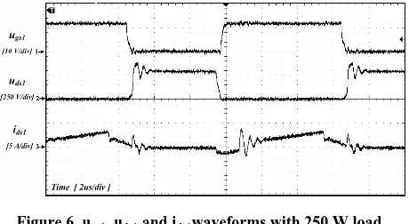
Figure 6. ugs1 ,uds1 and ids1waveforms with 250 W load.
Figure 7. ugs3 ,uds3 and ids3 waveforms with 450 W load.
but only hard switching on as uds3 drops to 100 V. The measured efficiency of this TTPP converter at full load is 94.8%.
5. Conclusions
A TTPP converter which can achieve ZVS is presented in this paper. It only requires an extra transistor to be inserted between the input power source and midpoint of two primary windings in traditional push-pull converter. Adopting phase-shifting concept, the logic of the three driving signals is similar to that in phase-shift full-bridge converter. So this TTPP converter has a similar operation theory as phase-shifting full-bridge converter. Its two primitive power switches can obtain wide range ZVS. The extra power switch can achieve ZVS based on the energy of the leakage inductance. Its transformer wave-form is as same as that in phase-shifting full-bridge cir-cuit. As a result, this TTPP converter has a characteristic between traditional push-pull converter and phase-shift- ing full-bridge converter. It could be applied in many fields.
6. Acknowledgements
This work is supported by National Natural Science Foundation of China (51067004), Key Science and Technology Project of Jiangxi Province of China (2010BGA02000) and Science and Research Foundation of Educational Department of Jiangxi Province in China (GJJ12293).
REFERENCES
[1] W. Chen, F. C. Lee, M. M. Jowanovic and J. A. Sabatec, “A Comparative Study of a Class of Full Bridge Ze-ro-voltage-switched PWM Converter,” in Proceedings of IEEE APEC, Dallas, USA, 1995, pp. 893-895.
[2] X. K. Wu, X. G Xie, C. Zhao, Z. M. Qian and R. X. Zhao, “Low Voltage and Current Stress ZVZCS Full Bridge DC–DC Converter Using Center Tapped Rectifier Reset,”
IEEE Transactions Industry Electronics, Vol. 55, 2008, pp. 1470 - 1477.
[3] I. H. Cho, K. M. Cho, J. W. Kim and G. W. Moon, “A New Phase-Shifted Full-Bridge Converter with Maximum Duty Operation for Server Power System,” IEEE Trans-actions on Power Electronics, Vol. 26, 2011, pp. 3491-3500.
[4] Y. Jang and M. M. Jovanovic, “A New PWM ZVS Full-Bridge Converter,” IEEE Transactions on Power Electronics, Vol. 22, 2007, pp. 987-994.
doi:10.1109/TPEL.2007.897008
[5] X. K. Wu, X. G. Xie, J. M Zhang, R. X. Zhao and Z. M. Qian, “Soft Switched Full Bridge DC–DC Converter With Reduced Circulating Loss and Filter Requirement, ”
IEEE Transactions on Power Electronics, Vol. 22, 2007, pp. 1949-1955. doi:10.1109/TPEL.2007.904211
[6] H. K. Yoon, S. K. Han, J. S. Park, G. W. Moon and M. J. Youn, “Zero-Voltage Switching Two-Transformer Full-Bridge PWM Converter With Lossless Diode-Clamp Rectifier for PDP Sustain Power Module, ” IEEE Trans-actions on Power Electronics, Vol. 21, 2011, pp. 1243-1252.doi:10.1109/TPEL.2006.880346
[7] B. Yang , F. C. Lee and A. J. Zhang, et al., “LLC Reso-nant Converter for Front End DC/DC Conversion,” in
Proceedings of IEEE APEC, Dallas, USA, 2002, pp. 1108-1112.
[8] I. O. Lee and G. W. Moon, “Analysis and Design of a Three-Level LLC Series Resonant Converter for High- and Wide-Input-Voltage Applications,” IEEE Transac-tions on Power Electronics, Vol. 27, 2012, pp. 2966-2979. doi:10.1109/TPEL.2011.2174381
[9] X. G. Xie, J. M. Zhang, C. Zhao, Z. Zhao and Z. M. Qian, “Analysis and Optimization of LLC Resonant Converter With a Novel Over-Current Protection Circuit,” IEEE Transactions on Power Electronics, Vol. 22, 2007, pp. 435-443.
[10] K. Y. Yi and G. W. Moon, “Novel Two-Phase Interleaved LLC Series-Resonant Converter Using a Phase of the Resonant Capacitor,” IEEE Transactions on Industrial Electronics, Vol. 56, 2009, pp. 1815-1819.
doi:10.1109/TIE.2008.2011310
[11] Y. L. Gu, Z. Y. Lu, L. J. Hang, Z. M. Qian and G. S. Huang, “Three-level LLC series resonant DC/DC con-verter,” IEEE Transactions on Power Electrionics, Vol. 20, 2005, pp. 781-789. doi:10.1109/TPEL.2005.850921 [12] M. Xu, Y. C. Ren, J. H. Zhou and F. C. Lee, “1-MHz
Self-driven ZVS Full-bridge Converter for 48-V Power Pod and DC/DC Brick,” IEEE Transactions on Power Electronics, Vol. 20, 2005, pp. 997-1006.
Push-pull DC/DC Converter Topology,” in Proc.IEEE APEC Dallas, USA, 2002, pp. 1097-1100.
[14] Y. S. Yuan, J. Y. Shu and Q. F. Wu, “N-period Resonant Behaviour of a Soft-switching Push-pull Conveter,” in
Proceedings of IEEE-ISIE, Hangzhou, China, 2012, pp. 397-401.
[15] M. J. Ryan, W. E. Brumsickle, D. M. Divan and R. D. Lorenz, “A New ZVS LCL-resonant Push-pull DC-DC Converter Topology,” IEEE Transactions on Industry Applications, 1998, pp. 1164-1174.
doi:10.1109/28.720458
[16] Y. S. Yuan, M. Chen and Z. M. Qian, “A Parallel Front-End LCL Resonant Push-Pull Converter with a Coupled Inductor for Automotive Applications,” in Pro-ceedings of IEEE APEC, Palm Springs, USA, 2010, pp. 1460-1463
[17] H. Ma, H. X. Yu and Y. Y. Yan, “Investigation on LCL Resonant Converter as Current Source,” in Proceedings of CSEE, Vol. 29, No. 9, 2009, pp. 28-34
[18] W. Chen, Z. Y. Lu, X. F. Zhang, et al., “ A Novel ZVS Step-up Push-pull Type Isolated LLC Series Resonant DC-DC Converter for UPS Systems and Its Topology Variations,” in Proceedings of IEEE APEC, Austin, USA, 2008, pp. 1073-1078.
[19] T. F. Wu, J. C. Hung, J. Z. Tsai and Y. M. Chen, “An Active-clamp Push-pull Converter for Battery Sourcing Application,” IEEE transactions on Industry Applications,
Vol.44, 2008, pp.196-204.