ii
DUAL-BAND MICROSTRIP LOOP ANTENNA FOR WIRELESS
APPLICATION
AHMAD MABROOK ALI SAAD
This project report presented in partial Fulfillment of the requirements for the award of The Degree of Master of Electrical Engineering
Faculty of Electrical and Electronic Engineering UniversitiTun Hussein Onn Malaysia
ABSTRACT
vii
ABSTRAK
Dalam tahun-tahun kebelakangan ini, microstrip dan antenna dicetak digunakan secara meluas bagi memenuhi keperluan komersial. Kemunculan aplikasi tanpa wayar memerlukan padat antenna pembuatan mudah. Tujuan projek ini adalah untuk mereka bentuk band antenna gelung dua microstrip untuk aplikasi tanpa wayar dengan pengurangan dalam saiz. Tujuan antenna ini adalah untuk beroperasi dari 2 GHz 4 GHz. Sebuah antenna patch microstrip persegi telah dipilih sebagai corak reka bentuk antenna kerana struktur rendah profil. Pembangunan projek ini terdiri daripada dua peringkat utama di mana tahap pertama adalah simulasi perisian (CST Microwave Studio) dan kedua adalah pembangunan perkakasan. CST Microwave Studio telah digunakan untuk meniru reka bentuk antenna untuk tujuan reka bentuk awal yang sedia ada kelebihan antenna boleh dikenal pasti, maka peringkat kedua ialah pembangunan antena patch microstrip yang telah direka pada FR4 substrat dan diuji dengan menggunakan penganalisis rangkaian yang mempunyai pelbagai antara untuk 1GHz untuk 14GHz. Berdasarkan projek ini, parameter antenna seperti kehilangan kembali, corak sinaran, nisbah gelombang pegun voltan (VSWR) dan jalur lebar telah disiasat. Untuk siasatan lanjut, bahan substrat dengan pemalar dielektrik yang lebih tinggi boleh digunakan untuk mengurangkan saiz antenna mikrostrip. Prestasi antena dual band menunjukkan perjanjian antara kedua-dua simulasi dan keputusan ukuran.
TABLE OF CONTENTS
TITLE ii
DECLARATION iii
DEDICATION iv
ACKNOWLEDGEMENT v
ABSTRACT vi
ABSTRAK vii
TABLE OF CONTENTS viii
LIST OF TABLE xiii
LIST OF FIGURE xiv
LIST OF SYMBOLS AND ABBREVIATIONS xix
LIST OF APPENDIX xx
CHAPTER I INTRODUCTION 1
1.1 Project Background 1
1.2 Problem statement 3
1.3 Project Objectives 3
1.4 Project Scopes 3
1.5 Thesis Outline 4
1.6 Chapter summary 4
CHAPTER IILITERATURE REVIEW 6
2.1 Overview 6
2.2 Background of Microstrip Antenna 6
2.2.1 Literature study 9
2.2.2 Advantages and Disadvantages 9
2.2.3 Feed Techniques 10
ix
2.3.1 Radiation pattern 11
2.3.1.1 Principal Patterns 11
2.3.1.2 Radiation pattern lobes 11
2.3.2 Directivity 12
2.3.3 Gain 13
2.3.4 Half-power beamwidth 14
2.3.5 Bandwidth 14
2.3.6 Input impedance 15
2.3.7 Polarization 16
2.3.8 Reflection coefficient 16
2.3.9 Voltage Standing Wave Ratio (VSWR) and
Return Loss 17
2.4 Analysis for Transmission Line Model 18
2.4.1 Coaxial Probe Feed 20
2.5 Technology Development 21
2.5.1 Application: PCS 21
2.5.2 Application: UMTS 21
2.5.3 Application: IMT-2000 22
2.5.4 Application: WiMax 22
2.6 Wireless Local Area Network (WLAN) 22
2.7 Research Paper Literature Review 23
2.8 Related Works 23
2.9 Chapter Summary 27
CHAPTER IIIMETHODOLOGY 28
3.1 Introduction 28
3.2 Design and specifications 32
3.2.1 Dual band patch antenna design 32
3.2.2 Signal feed 35
3.2.3 Substrate 36
3.3 CST Microwave Studio 36
3.4 Fabrication process 36
3.4.2 Lamination and UV light process 38
3.4.3 Developing process 39
3.4.4 Etching Process 40
3.4.5 Stripping process 40
3.4.6 Soldering Process 41
3.5 Antenna measurement 41
3.6 Chapter summary 43
CHAPTER IVRESULT AND ANALYSIS 44
4.1 Introduction 44
4.2 Antenna Geometry Construction Steps 44
4.3 Simulation Result 47
4.3.1 Return Loss, S11 (dB) 47
4.3.1.1 Loop angle 90 degree 47
4.3.1.2 Loop angle 80 degree 48
4.3.1.3 Loop angle 70 degree 49
4.3.1.4 Loop angle 60 degree 49
4.3.2 Bandwidth 51
4.3.2.1 Loop angle 90 degree 51
4.3.2.2 Loop angle 80 degree 52
4.3.2.3 Loop angle 70 degree 53
4.3.2.4 Loop angle 60 degree 54
4.3.3 Voltage Standing Wave Ratio (VSWR) 56
4.3.3.1 Loop angle 90 degree 56
4.3.3.2 Loop angle 80 degree 56
4.3.3.3 Loop angle 70 degree 57
4.3.3.4 Loop angle 60 degree 57
4.3.4 Input Impedance 59
4.3.4.1 Loop angle 90 degree 59
4.3.4.2 Loop angle 80 degree 60
4.3.4.3 Loop angle 70 degree 60
4.3.4.4 Loop angle 60 degree 61
xi
4.3.5.1 Loop angle 90 degree 62
4.3.5.2 Loop angle 80 degree 64
4.3.5.3 Loop angle 70 degree 66
4.3.5.4 Loop angle 60 degree 68
4.3.6 Gain 70
4.3.6.1 Loop angle 90 degree 70
4.3.6.2 Loop angle 80 degree 72
4.3.6.3 Loop angle 70 degree 73
4.3.6.4 Loop angle 60 degree 75
4.4 Measurement Results 77
4.4.1 Return Loss (S11) dB 77
4.4.1.1 Loop angle 90 degree 77
4.4.1.2 Loop angle 80 degree 78
4.4.1.3 Loop angle 70 degree 78
4.4.1.4 Loop angle 60 degree 79
4.4.2 Voltage Standing Wave Ratio (VSWR) 80
4.4.2.1 Loop angle 90 degree 80
4.4.2.2 Loop angle 80 degree 81
4.4.2.3 Loop angle 70 degree 81
4.4.2.4 Loop angle 60 degree 82
4.4.3 Input Impedance 83
4.4.3.1 Loop angle 90 degree 83
4.4.3.2 Loop angle 80 degree 83
4.4.3.3 Loop angle 70 degree 84
4.4.3.4 Loop angle 60 degree 85
4.5 Simulation and Measurement Result Analysis 85
4.5.1 Return Loss, S11 (dB) 86
4.5.2 Voltage Standing Wave Ratio (VSWR) 87
4.6 Chapter Summary 88
CHAPTER V CONCLUSION AND RECOMMENDATION 89
5.1 Introduction 89
5.3 Recommendation 91
REFERENCES 92
xiii
LIST OF TABLE
3.1 Dual band patch antenna parameters 35
3.2 FR4 substrate specifications 36
4.1 Operating frequency, return loss and bandwidth of the dual
frequency patch antenna 55
4.2 the percentage of error between simulated and measured results
for return loss 86
LIST OF FIGURE
2.1 Rectangular and circular (patch) microstrip antenna 7
2.2 Microstrip Patch Antenna Structure 8
2.3 Coaxial Feed 10
2.4 Radiation pattern of a generic directional antenna 12
2.5 Antenna bandwidth 14
2.6 6A rectangular microstrip patch antenna showing fringing
fields that account for radiation 18
2.7 A patch excited using coaxial probe. 18
2.8 Choice of feed point for a probe fed-patch 20
3.1 Flowchart of the overall project 29
3.2 Flowchart of the antenna design 31
3.3 structure of the proposed antenna:
(a)Top view and (b) Side view 33
3.4 Photograph of the antenna prototype 34
3.5 Photograph of the antenna prototype with different
angles () fabricated on FR4 34
3.6 SMA connector - Socket SMA Panel 35
3.7 Flowchartforthefabricationprocess 37
3.8 Printed layoutof dual band Patch Antenna 38
3.9 laminating process 38
3.10 Lamination machine 38
3.11 UV exposure units 39
3.12 Developing machine 39
3.13 Etching machine 40
3.14 Stripping machine 40
3.15 Fabricated dual frequency patch antenna 41
xv
3.17 Antenna measurement using ZVB 14 vector network
analyzer 42
4.1 (a) Substrate design 45
4.1(b) Antenna patch design 45
4.1 (c) Antenna patch design 46
4.1 (d) Ground plane design (left side) 46
4.1 (e) Ground plane design (right side) 46
4.1 (f) Coaxial feed designs 47
4.2 (a) Simulated S11 result for dual frequency antenna
(loop angle 90°) 48
4.2 (b) Simulated S11 result for dual frequency antenna
(loop angle 80°) 48
4.2 (c) Simulated S11 result for dual frequency antenna
(loop angle 70°) 49
4.2 (d) Simulated S11 result for dual frequency antenna
(loop angle 60°) 50
4.2 (e) Simulated S11 result for dual frequency antenna for various
loop angle 50
4.3 (a) Bandwidth of the first operating frequency, 1.935 GHz 51 4.3 (b) Bandwidth of the second operating frequency,3.7476 GHz 52 4.3 (c) Bandwidth of the first operating frequency, 1.945 GHz 52 4.3 (d) Bandwidth of the second operating frequency,3.7558 GHz 53 4.3 (e) Bandwidth of the first operating frequency, 1.977 GHz 53 4.3 (f) Bandwidth of the second operating frequency,3.8996 GHz 54 4.3 (g) Bandwidth of the second operating frequency,4.1169 GHz 54 4.4 (a) Simulated voltage standing wave ratio (VSWR)
(loop angle 90°) 56
4.4 (b) Simulated voltage standing wave ratio (VSWR)
(loop angle 80°) 57
4.4 (c) Simulated voltage standing wave ratio (VSWR)
(loop angle 70°) 57
4.4 (d) Simulated voltage standing wave ratio (VSWR)
4.4 (e) Simulated (VSWR) result for dual frequency antenna for
various loop angles 58
4.5 (a) Simulated input impedance for dual frequency patch antenna
(loop angle 90°) 59
4.5 (b) Simulated input impedance for dual frequency patch antenna
(loop angle 80°) 60
4.5 (c) Simulated input impedance for dual frequency patch antenna
(loop angle 70°) 61
4.5 (d) Simulated input impedance for dual frequency patch antenna
(loop angle 60°) 61
4.6 (a) Radiation pattern at 1.94 GHz of the antenna in 2D view
(loop angle 90°) 62
4.6 (b) Radiation pattern at 1.94 GHz of the antenna in 3D view
(loop angle 90°) 63
4.7 (a) Radiation pattern at 2.4 GHz of the antenna in 2D view (loop
angle 90°) 63
4.7 (b) Radiation pattern at 2.4 GHz of the antenna in 3D view (loop
angle 90°) 64
4.8 (a) Radiation pattern at 1.945 GHz of the antenna in 2D view
(loop angle 80°) 64
4.8 (b) Radiation pattern at 1.94 5GHz of the antenna in 3D view
(loop angle 80°) 65
4.9 (a) Radiation pattern at 3.755 GHz of the antenna in 2D view
(loop angle 80°) 65
4.9 (b) Radiation pattern at 3.755GHz of the antenna in 3D view
(loop angle 80°) 66
4.10 (a) Radiation pattern at 1.9941 GHz of the antenna in 2D view
(loop angle 70°) 66
4.10 (b) Radiation pattern at 1.9941 GHz of the antenna in 3D view
(loop angle 70°) 67
4.11 (a) Radiation pattern at 3.9061 GHz of the antenna in 2D view
xvii
4.11 (b) Radiation pattern at 3.9061GHz of the antenna in 3D view
(loop angle 70°) 68
4.12 (a) Radiation pattern at 2.081 GHz of the antenna in 2D view
(loop angle 60°) 68
4.12 (b) Radiation pattern at 2.081 GHz of the antenna in 3D view
(loop angle 60°) 69
4.13 (a) Radiation pattern at 4.1169 GHz of the antenna in 2D view
(loop angle 60°) 69
4.13 (b) Radiation pattern at 4.1169 GHz of the antenna in 3D view
(loop angle 60°) 70
4.14 (a) Antenna gain at 1.94 GHz in 2D view (loop angle 90°) 70 4.14 (b) Antenna gain at 1.94 GHz in 3D view (loop angle 90°) 71 4.15 (a) Antenna gain at 3.74 GHz in 2D view (loop angle 90°) 71 4.15 (b) Antenna gain at 3.74 GHz in 3D view (loop angle 90°) 71 4.16 (a) Antenna gain at 1.945 GHz in 2D view (loop angle80°) 72 4.16 (b) Antenna gain at 1.945 GHz in 3D view (loop angle80°) 72 4.17 (a) Antenna gain at 3.7558 GHz in 2D view (loop angle 80°) 73 4.17 (b) Antenna gain at 3.7558 GHz in 3D view (loop angle 80°) 73 4.18 (a) Antenna gain at 1.9944 GHz in 2D view (loop angle 70°) 74 4.18 (b) Antenna gain at 1.9944 GHz in 3D view (loop angle 70°) 74 4.19 (a) Antenna gain at 1.9061 GHz in 2D view (loop angle 70°) 74 4.19 (b) Antenna gain at 1.9061 GHz in 3D view (loop angle 70°) 75 4.20 (a) Antenna gain at 2.081 GHz in 2D view (loop angle 60°) 75 4.20 (b) Antenna gain at 2.081 GHz in 3D view (loop angle 60°) 76 4.21 (a) Antenna gain at 4.1169 GHz in 2D view (loop angle 60°) 76 4.21 (b) Antenna gain at 4.1169 GHz in 3D view (loop angle 60°) 76 4.22 Measured return loss, S11 (dB) (loop angle 90°) 77 4.23 Measured return loss, S11 (dB) (loop angle 80°) 78 4.24 Measured return loss, S11 (dB) (loop angle 70°) 79 4.25 Measured return loss, S11 (dB) (loop angle 60°) 79 4.26 Measured S11 result for dual frequency antenna for
various loop angle 80
angle 90° 80 4.28 Measured voltage standing wave ratio (VSWR) with loop
angle 80° 81
4.29 Measured voltage standing wave ratio (VSWR) with loop
angle 70° 81
4.30 Measured voltage standing wave ratio (VSWR) with loop
angle 60° 82
4.31 Measured (VSWR) result for dual frequency antenna for
various loop angles 82
4.32 Input impedance of the measured dual band patch antenna
(loop angle 90°) 83
4.33 Input impedance of the measured dual band patch antenna
(loop angle 80°) 84
4.34 Input impedance of the measured dual band patch antenna
(loop angle 70°) 84
4.35 Input impedance of the measured dual band patch antenna
(loop angle 60°) 85
xix
LIST OF SYMBOLS AND ABBREVIATIONS
c Speed of light
D Directivity
E Efficiency
f Operating frequency
fc Center frequency
fH Upper frequency
fL Lower frequency
G Gain
h Substrate thickness
L Length
Leff Effective length
Rin Antenna resistance
S11 Return loss or Reflection Coefficient (dB)
Xin Antenna reactance
W Width
Zin Input impedance
Zo Characteristic impedance
Free space wavelength
r
Dielectric constant
L
Extended length due to fringing field effect
Reflection coefficientdB Decibel
HPBW Half power beamwidth
PCB Printed circuit board
RL Return loss
SWR Standing wave ratio
LIST OF APPENDICES
APPENDIX TITLE PAGE
A Gantt chart 94
GANTT CHART FOR PS 1 94
CHAPTER I
INTRODUCTION
1.1 Project Background
Wireless communication devices have been playing a very important part in our daily life, especially for the past ten years. Due to this reason, antennas designed for wireless applications have attracted much attention from researchers all over the world. Multiband antennas are able to provide multiple reception and transmission functionalities. It is therefore much desirable to have a single antenna using a single feed point that covers multiple frequency bands. The designed antennas are expected to be compact and simple and such as to be integrated well with other communication devices. The printed antenna is well-known for its compactness, low cost, ease of manufacturing and ease of integration with other circuits.
Today we have a number of land and satellite based systems for wireless communications using a wide range of frequency bands. Not only do we see an increase in the number of subscribers in the different systems but also a demand for dual or multi band equipment capable of handling two or more frequency bands
standards for WLAN is needed. In recent years, some dual-band antennas for WLAN application have proposed. However, these researches cannot cover all of the WLAN frequencies.
Many microstrip printed antennas have been reported for wireless communication applications. The antennas are somewhat complicated with many design dimensions. This results in a somewhat complicated fabrication procedure, with the consequence that even small changes in the dimensions could affect the antenna operating frequency. Double-sided antennas are proposed to cope the need for fabrication precision, as both sides of the antenna have to be properly aligned. The antenna proposed by Li [1] requires careful fabrication as the balun on the other side of the antenna is not symmetrical.
Nowadays, microstrip–fed printed monopole antennas play a key role in WLAN applications because of their attractive features, such as low profile, low cost, light weight, and are suitable for integration with MMICs and active devices.
The worldwide growth of personal wireless communication devices has been tremendous. One of the trends in wireless mobile technology in the last decade has been to dramatically decrease the size and the weight of the handset. With this progress in mobile terminal size reduction, the design of antennas is acquiring even greater importance. Antennas must be small, and yet achieve specified electrical performance, such as wide bandwidth, operation in dual or triple frequency bands, diversity, and so forth. Accordingly, antenna designers have encountered difficulty in designing antennas that can maintain electrical performance characteristics while being reduced in size because, in general, efficiency and bandwidth degrade with size decrease.
1.2 Problem statement
3
radio network is to find suitable sites for the base stations, one can expect these operators to use their existing sites for the new 1800 or 1900 MHz base station wherever possible. Then, one possibility is to replace an existing GSM or AMPS antenna with a dual band GSM/DCS or AMPSPCS antenna. In this will present an antenna element suited for the GSM/DCS bands, i.e. 880-960 MHz and 1710-1880MHz.A dual band base station antenna would have a linear array of such elements positioned along the vertical axis.
1.3 Project Objectives
The objective of this proposed research is as follow:
To design a dual band microstrip antenna this will be operating in the wireless LAN band, IEEE 802.11 a/b/g. The dimensions of the single elements of the operating frequencies were calculated using transmission line model.
To achieve a techniques for dual band or multiband antenna using 2 element of square patch microstrip antenna using inset feed for each frequency band at 2.4 GHz band and 3.8 GHz band.
1.4 Project Scopes
For the overview of the project, the project scopes focusing on four major components which represent as follows:
i) The antenna is intended to be operated at 2 GHz and 3.8 GHz for wireless application such as, PCS, UMTS , IMT-2000 and WiMax.
iii) Some of antenna parameters will be studied in this project such as radiation pattern, gain, reflection coefficients, return loss (S11) , VSWR , bandwidth and so
on.
iv) The square microstrip patch antenna will be tested by using Network Analyzer. The device has good performance and it is available in the university.
1.5 Thesis Outline
The thesis outline has been arranged as follows. Chapter II describes about the theory of the dual band patch antenna, antenna properties and also explains about the researches that have been done associated to this project.
Chapter III of this thesis explains about the methodology that has been used in order to complete this project. Details about the software and equipment’s that has been used also were described.
Chapter IV of this thesis describes about the simulation and measurement that has been obtained. Analyses for both of the results were also explained.
Lastly, Chapter V explains several recommendations to upgrade this project. Overall conclusion for this project also has been stated.
1.6 Chapter summary
5
CHAPTER II
LITERATURE REVIEW
2.1 Overview
This chapter reviews some similar previous work, related journals and researches that include dual frequency antenna designs that can contribute in ideas for completing this project.
2.2 Background of Microstrip Antenna
7
mechanically robust when mounted on rigid surfaces, compatible with MMIC design, are very versatile in terms of resonant frequency, polarization and impedance.
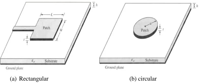
[image:23.612.133.524.149.313.2](a) Rectangular (b) circular Figure 2.1 Rectangular and circular (patch) microstrip antenna.
Microstrip is a planar transmission line, similar to stripline and coplanar waveguide. Microstrip was developed by ITT Telecommunications Laboratories in Nutley New Jersey, as a competitor to strapline. According to Pozar [2] early microstrip work used fat substrates, which allowed non-TEM waves to propagate which makes results unpredictable. In the 1960s, the thin version of microstrip became popular.
By 1955, ITT had published a number of papers on microstrip in the IEEE transactions on microwave theory and technique. A paper by M. Arditi titled “characteristics and applications of microstrip for microwave wiring” is a good one [2].
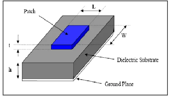
Figure 2.2 Microstrip Patch Antenna Structure.
Based on the Figure 2.2, it shows the common microstrip patch antenna structure. L is the length of the patch, W is the width of the patch, h is the height of the patch and t is the patch thickness.
To achieve great antenna performance, thick dielectric substrate having low dielectric constant is needed. This will provide higher efficiency, larger bandwidth and greater radiation. But, in order to achieve this, larger antenna size will be needed. So, in order to produce a compact design, higher dielectric constant which are less efficient and will contribute to narrower bandwidth will be used [3].
Microstrip antenna has several advantages compared to conventional microwave antenna. These types of antennas are light weight, low volume and thin profile configurations, which can be made conformal. The cost of fabrication is also low. So, it can be manufactured in large quantities [3]. For the polarization types, it can support both linear and circular polarization depending on the radiation pattern. Microstrip patch antennas also are capable of dual and even triple frequency operations [3].
9
2.2.1 Literature study
This section provides an overview of various microstrip antenna design and applications. The purpose of this overview is to summarize the main development in the area of Dual-Band Microstrip Loop Antenna in the past several decades and reveal the motivation of this research.
Nowadays most preferred type of antenna for communication are microstrip antennas because of their lucrative features such as small size, light weight, low cost, conformability to planar and non-planar surfaces, rigid, and easy installation. They have a wide range of application in wireless communication especially in mobile communications devices and are becoming more general due to low cost and versatile designs. Recently, dual-band cellular phones capable of operating in two different cellular systems are increasing [3].
2.2.2 Advantages and Disadvantages
Microstrip antennas are used as embedded antennas in handheld wireless devices such as cellular phones, and also employed in satellite communications. Some of their principal advantages are given below:
Light weight and low fabrication cost.
Supports both, linear as well as circular polarization.
Can be easily integrated with microwave integrated circuits. Capable of dual and triple frequency operations.
Mechanically robust when mounted on rigid surfaces.
Narrow bandwidth. Low efficiency and Gain.
Extraneous radiation from feeds and junctions. Low power handling capacity.
Surface wave excitation.
2.2.3 Feed Techniques
Microstrip antenna feed techniques can be categorized in two categories which are contacting and non-contacting. In the contacting method, the RF Power is fed directly to the radiating patch using a connecting element such as a microstrip line. The microstrip line and the coaxial probe are examples of contacting method. In the non-contacting, electromagnetic field coupling will be done to transfer the power between the microstrip line and the radiating patch. Techniques that are in these non-contacting methods are aperture coupling and proximity coupling [3].
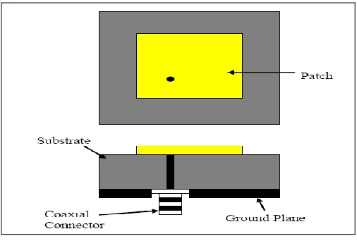
[image:26.612.219.472.504.675.2]The feed technique that was used in this project is the coaxial feed. This feed method is easy to fabricate. The feed can be placed at any location to match with its input impedance. However, it provides narrow bandwidth and it is difficult to model. Figure 2.3 below shows the coaxial feed [3].
11
2.3 Antenna Properties
The performance of the antenna can be determined by these important parameters.
2.3.1 Radiation pattern
It is defined as a mathematical function or a graphical representation of the radiation properties of the antenna as a function of space coordinates. The radiation property of most concern is the two or three-dimensional spatial distribution of radiated energy as the function of the observer’s position along a path of surface of constant radius [4].
2.3.1.1 Principal Patterns
For a linearly polarized antenna, the performance is usually described in terms of its principal E- and H-plane patterns. The E-plane is defined as the plane containing the electric-field vector and the direction of maximum radiation.
The H-plane is defined as the plane containing the magnetic-field vector and the direction of maximum radiation [4].
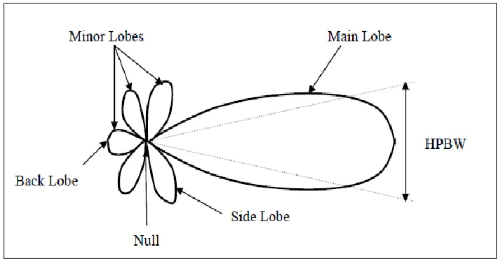
2.3.1.2 Radiation pattern lobes
Figure 2.4: Radiation pattern of a generic directional antenna.
2.3.2 Directivity
It can be defined as the ratio of the radiation intensity in a given direction from the antenna to the radiation intensity averaged of all directions. The average radiation intensity is equal to the total power radiated by the antenna divided by 4π. If the direction is not specified, the direction of maximum radiation intensity is implied [4].
If the direction is not specified, the direction of maximum radiation intensity can be expressed as:
Dmax = Do =
rad max 4
max P U Uo
U
(2.1) Where:
D = directivity (dimensionless)
Do = maximum directivity (dimensionless) U = radiation intensity (W/unit solid angle)
Umax = maximum radiation intensity (W/unit solid angle)
13
Reference antennas usually are isotropic radiator where the radiated energy is the same in all direction and have directivity of 1. It can be defined as:
D= Fo Fmax (2.2) Where:
Fmax = maximum radiated energy Fo = isotropic radiator radiated energy
2.3.3 Gain
Gain is closely related to directivity but it is a measure that takes into account the efficiency of the antenna and also the directional capabilities. Absolute gain of an antenna in a given direction is defined as the ratio of the intensity, in a given direction, to the radiation intensity that would be obtained if the power accepted by the antenna were radiated isotropically. The radiation intensity corresponding to the isotropically radiated power is equal to the power accepted by the antenna divided by 4π [4].
It also can be expressed as:
Gain =
Pin U
4 ,power (accepted) input total intensity radiation
4 (2.3)
For a lossless isotropic source,
G= source) isotropic lossless ( ) , ( 4 Pin
U
2.3.4 Half-power beamwidth
It can be defined as in a plane containing the direction of the maximum of a beam, the angle between the two directions in which the radiation intensity is one-half of the maximum value of the beam. It is used to describe the 3dB beamwidth. As the beamwidth decreases, the sidelobe increases and vice versa [4]. Antenna gain is inversely proportional to the beamwidth ; the higher the gain, the narrower the antenna beamwidth [4].
2.3.5 Bandwidth
[image:30.612.176.505.450.616.2]The term bandwidth is defined as the range of frequencies within which the performance of the antenna, with respect to some characteristic, conforms to a specified standard. For narrowband antenna, the bandwidth is expressed as a percentage of the frequency difference over the center frequency of bandwidth. The characteristics such as input impedance, gain and polarization of antenna do not necessarily affect the frequency.
Figure 2.5 Antenna bandwidth
15
bandwidth are used to emphasize this distinction. Gain, side lobe level, beamwidth, polarization and beam direction are associated with pattern bandwidth while input impedance and radiation efficiency are associated with impedance bandwidth [4].
Narrowband by percentage can be expressed by:
BW =
frequency operating frequency off -cut Lower frequency off -cut
Higher
x 100% (2.5)
2.3.6 Input impedance
It is defined as the impedance presented by an antenna at its terminals or ratio of the voltage to current at a pair of terminals or the ratio of the appropriate components of the electric to magnetic fields at a point. The input impedance can be determined by the maximum power transfer between transmission line and the antenna. When the input impedance, antenna and transmission line are matched, maximum power transfer will be achieved. Reflected wave will be generated at the antenna terminal and travel back towards the energy source if it is not matched. It will cause reduction on the overall system efficiency [4].
The input impedance can be described as:
Z1=
11 11 S 1 1 S
Zo (2.6)
Where:
Z1= n input impedance
2.3.7 Polarization
Polarization of an antenna in a given direction is defined as the polarization of the wave transmitted (radiated) by the antenna. The polarization of a wave can be defined in terms of a wave radiated or received by an antenna in a given direction. The polarization of a wave radiated by an antenna in a specified direction at a point in the far field is defined as the polarization of the plane wave whose electric field strength is the same as that of the wave and whose direction of propagation is in the radial direction from the antenna [4].
Polarization can be classified as linear, circular and elliptical. The field is said to be linearly polarized if the vector that describes the electric field at a point in space as a function of time is always directed along a line. If the electric field traces is an ellipse, the field is elliptically polarized. For circular polarization, a time-harmonic wave is circularly polarized at a given point in space if the electric field or magnetic field vector at that point traces a circle as a function of time [4].
Polarization characteristics of an antenna can be represented by its polarization pattern which is defined as the spatial distribution of the polarizations of a field vector excited by an antenna taken over its radiation sphere [4].
2.3.8 Reflection coefficient
Determining the value of the input reflection coefficient of the antenna is necessary to determine the location of the resonant bands. The input reflection coefficient, Гin, is obtained from expression below [4]:
Гin =
Zo Zin
Zo Zin
(2.7) Where
Zin =input impedance of the antenna
17
The absolute value of the reflection coefficient can be also expressed as the ratio of the reflected power from the antenna input, Pin and the power delivered to the antenna, Pin as in expression below [4]:
in ref P P in
(2.8)
2.3.9 Voltage Standing Wave Ratio (VSWR) and Return Loss
When a load is mismatched to a transmission line, not all power from the generator will be delivered to the load. The loss is called return loss and expressed as:
RL= -20 log dB (2.9)
A matched load, where the reflection coefficient, Г=0, has return loss of ∞ dB, whereas a total reflection of all power, where Г=1, has a return loss of 0 dB. In a mismatched line, the presence of reflected wave leads to standing wave, where the magnitude of the voltage oscillates along the line.
As the value of reflection coefficient increases, the ratio of the minimum and maximum voltage values (v max and v min) also increases. So, the Voltage Standing Wave Ratio (VSWR) measures the ratio of these voltages on a transmission line. It can be expressed as:
SWR= 11 11 1 1 1 1 min max S S V V (2.10)
2.4 Analysis for Transmission Line Model
[image:34.612.204.451.263.406.2]The patch and ground-plane are separated by a dielectric. The patch conductor is normally copper. The patches are usually photo-etched on the dielectric substrate. The substrate is usually non-magnetic. The relative permittivity of thesubstrate is normally in the region between 1and 4, which enhances the fringing fields [5]. The rectangular patch is characterized by its length L, width w and thickness h, as shown in Figure 2.6 below.
Figure 2.6A rectangular microstrip patch antenna showing fringing fields that account for radiation.
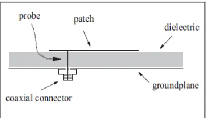
The inner conductor of the coaxial-line is connected to the radiating patch, while the outer conductor is connected to the ground-plane, as shown in Figure 2.7 below.
[image:34.612.225.431.566.684.2]19
An effective dielectric constant (εreff) must be obtained in order to account for the fringing and the wave propagation in the line. The value of εreffis slightly less thenεrbecause the fringing fields around the periphery of the patch are not confined in the dielectric substrate but are also spread in the air. It can be expressed by [6]:
2 1 12 1 2 1 2 1 w h r r
reff
(2.11)
Where
εreff= Effective dielectric constant
εr= Dielectric constant of substrate
h = Height of dielectric substrate W = Width of patch
For a given resonance frequency fo, the effective length is given by [6]:
reff fo c Leff 2 (2.12)
The fringing fields along the width can be modeled as radiating slots and electrically the patch of the microstrip antenna looks greater than its physical dimensions. The dimensions of the patch along its length have now been extended on each end by a distance, ΔL.
The ΔL can be expressed as [6]:
ΔL = 0.412h
8 . 0 264 . 0 258 . 0 3 . 0 h W h W reff reff (2.13)
Leff= L + 2ΔL Where
ΔL= Length due to fringing effects L = Length of patch
Leff=Effective length of the patch h = Height of dielectric substrate W = Width of patch
εreff= Effective dielectric constant
For efficient radiation the width, W is given by [6]:
2 1
2
r fo
c W
(2.14)
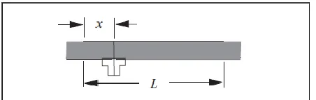
[image:36.612.234.460.444.516.2]2.4.1 Coaxial Probe Feed
Figure 2.8: Choice of feed point for a probe fed-patch.
21
Y (along the width) = 2 W
(2.15)
X (along the length) =
) ( 2 reff l
L
(2.16)
2.5 Technology Development
2.5.1 Application: PCS
Personal Communications Service or PCS describes a set of wireless communications capabilities that allows some combination of terminal mobility, personal, and service profile management [8]. More specifically, PCS refers to any of several types of wireless voice and wireless data communications systems, typically incorporating digital technology, providing services similar to advanced cellular mobile or paging services. In addition, PCS can also be used to provide other wireless communications services, including services that allow people to place and receive communications while away from their home or office, as well as wireless communications to homes, office buildings and other fixed locations. Described in more commercial terms, PCS is a generation of wireless-phone technology that combines a range of features and services surpassing those available in analog and digital-cellular phone systems, providing a user with an all-in-one wireless phone, paging, messaging, and data service [8].
2.5.2Application: UMTS
access technology to offer greater spectral efficiency and bandwidth to mobile network operators. UMTS specifies a complete network system which uses, covering the radio access network (UMTS Terrestrial Radio Access Network, or UTRAN), the core network (Mobile Application Part, or MAP) and the authentication of users via SIM (subscriber identity module cards). The technology described in UMTS is sometimes also referred to as Freedom of Mobile Multimedia Access (FOMA) [8] or 3GSM. Unlike EDGE (IMT Single-Carrier, based on GSM) and CDMA2000 (IMT Multi-Carrier), UMTS requires new base stations and new frequency allocations.
2.5.3 Application: IMT-2000
IMT-2000 is simply a term used by the International Telecommunications Union (ITU) to refer to many third generation (3G) wireless technology, that provide higher data speed between mobile phones and base antennas [8].
2.5.4 Application: WiMax
Worldwide Interoperability for Microwave Access (WiMAX ) is a "wireless" communications standard designed to provide 30 to 40 Mbps data rates [8], with the 2011 update providing up to 1 Gbps for fixed stations. The name "WiMAX" was created by the "WiMAX" forum, which was formed in June 2001 to promote conformity and interoperability of the standard. The forum describes WiMAX as a standards-based technology enabling the delivery of last mile wireless broadband access as an alternative to cable and DSL.
2.6 Wireless Local Area Network (WLAN)
23
are being setup in home and home office situations as the technology is becoming more affordable [9].
The increasing popularity of indoor wireless LAN capable of high-speed transfer rate is prompting the development of efficient broadband antennas. Due to increased usage in residential and office areas, these systems are required to be low profile, low cost as well as highly effective and efficient [9].
Microstrip patch antennas are well suited for wireless LAN application systems due to their versatility, conformability, low cost and low sensitivity to manufacturing tolerances. Conventionally, patch antennas have showed a narrowband response, implicating low bit rate transfer.
The most commonly used WLAN system is the IEEE 802.11b system, with maximum throughput of 11 Mbps using a narrowband system. Broadband refers to transmission of information using a system that uses a comparatively larger frequency band, resulting in increases data transfer rate or throughput. The broadband 802.11a system requires them to have a good coverage without failing signal strength. The range of coverage is dependent directly on the antenna performance hence the significance of the broadband antenna. A key requirement of a WLAN system is that it should be low profile, where it is almost invisible to the user. For this reason the microstrip patch antennas are the antennas of choice for WLAN use [9].
2.7 Research Paper Literature Review
The papers related to this title are chosen and studied. With the help from this literature review, it gives more clear understanding to perform this project.
2.8 Related Works
Universal Mobile Telecommunication System (UMTS 1.92-2.17 GHz), International Mobile Telecommunications-2000 (IMT 1.9-2.2 GHz), Industrial Scientific Medical (ISM 2.4-2.484 GHz) and Worldwide Interoperability for Microwave Access (WiMAX 3.49-3.79 GHz) wireless applications.
The achieved bandwidth was 36.4% at the lower frequency band and 11.8% at the higher frequency band. The antenna offers acceptable reflection coefficient and radiation pattern characteristics, as evidenced through measurement and simulation. This simple low-profile dual-band printed monopole antenna could be useful for PCS, UMTS, IMT, ISM and WiMAX wireless applications.
Mun et al [11] proposed and elaborated a novel dual band antenna for usage in WLAN compatible devices. This compact antenna was designed to form two different resonant paths in order to excite dual band resonance at 2.4 GHz and 5.2 GHz. The design was able to support the IEEE 802.11a/b/g bands completely at return loss less than -10 dB. Microstrip feeding technique was opted to accomplish planar structure. This antenna was capable to support wideband operation. At lower band and higher resonance band, the impedance bandwidth was 31.6% and 30.3%. The compactness and wideband characteristic associated with the proposed dual band antenna promotes employment in WLAN devices at ISM bands. A relatively high and constant gain was obtained at lower resonance band. Gain of 6.15 dB and 2.12 dB was obtained at 2.44 GHz and 5.21 GHz, respectively.
A dual-band monopole antenna fed by a 50 Ω microstrip transmission line was proposed by Hazeri and Azizkhani [12] for Wireless Local Area Network. The proposed microstrip–fed monopole antenna consists of a rectangular patch with four notches at the four corners of the rectangular patch and a small rectangular patch slot. For the microstrip-fed antenna, two resonant bands are seen. The first band was about 7% for the center frequency of 2.41 GHz and the second band extends from 4.876 to 6.2 GHz with a fractional bandwidth of 24%.
92
REFERENCES
[1] Liu W.C. and Chen W.R. CPW “fed compact meandered patch antenna for dual-band operation”, Electronics Letters, Vol. 40, Issue 18, pp.: 1094-1095, 2004.
[2] David.M.Pozar“microwave engineering”, 3rd edition Johnwiely and sons [3] Chapter 3,“Microstrip Patch Antenna ,Unpublished”, 2011.
[4] Constantine A.Balanis. “Antenna Theory”, 2nd Edition John Wiley & Sons, INC, Canada, 1997.
[5] J.R Jame,P.S Hall and C.Wood“Microstrip Antenna Theory and Design”, London, United Kingdom:Peter Peregrines Ltd.67-71,2006.
[6] Kraus, Marhefka“Antennas for All Application” 3rd.Ed McGraw-Hill, 2002.
[7] Vajha.S and Prasad,S.N.,“Design and Modelling of a Proximity Coupled Patch Antenna”,Conference of on Antenna and propagation for Wireless Communication.6-8 Nov.Massachusetts:IEEE-APS,43-46, 2000.
[8] http://en.wikipedia.org/wiki/Personal_Communications_Service.
[9] Mohammad Ilyas and Syed Ahson“Handbook of wireless local area networks : applications”, technology, security and standards,2008.
[10] Pei Cheng Ooi and Krishnasamy T. Selvan. “A Dual-Band CPW-Fed Printed Square Loop Antenna for Wireless Applications”, IEEE 978-1-4244-7368-7/10 ,2010. [11] Tan Yee Mun, Chan Yee Kit, Koo Voon Chet Mohammad TariqulIslamA“Novel Wideband Antenna for Dual Band WLAN Application”, IEEE 978-1-4244-7006-8/10.2010.
[14] Jiwei Han, Weiping Ding, Fei Chen,“Compact annular patch monopole antenna f or WLAN application”,.2010.
[15]Fong Chen and Chia-Mei Peng, “Microstrip-fed dual-U-shaped printed monopole antenna for dual-band wireless communication applications” ELECTRONICS LETTERS, Vol. 39 No. 13.26th June, 2003.
[16] A. Asrokin, M. K. A. Rahim, and M. Z. A. Abd.Aziz.,“Dual Band Microstrip Antenna for Wireless LAN Application”, Asia pacific conference on applied electromagnetic proceeding, Johor Bahru Johor, MALAYSIA,2005.
[17] Wiley. Periodicals, Inc. Microwave Opt TechnolLett, View this article online at wileyonlinelibrary.com. DOI 10.1002/mop.26226,2011.
[18] R.J. Lin, M. Ye.“A Novel Dual-Band Microstrip Antenna for WLAN Application”, School of Communication and Information Engineering, Shanghai University, Shanghai 200072, China,2009.
[19] V.Deepu, R. Sujith, S. Mridula.“ACS fed printed F-shaped uniplanar antenna for dual band WLAN applications”, Microwave and Optical Technology Letters, 51, pp.1852-1856.,2009.
[20] Vinod K. Singh, Zakir Ali, “Dual Band U- shaped microstrip antenna for wireless Communication” International Journal of Engineering Science and Technology Vol. 2(6),1623-1628 . ISSN: 0975-5462, 2010.
[21] Kim T.H. and Park D.C “CPW-fed compact monopole antenna for dual-band WLAN applications”, Electronics Letters, Vol. 41, Issue 6, 17 March 2005, pp.: 291-293, 2005.