Optimization of the Performance of Biosensor Based on
Photonic Crystal Resonant
Zahra Rostamikafaki
Alzahra University, Iran
Copyright©2019 by authors, all rights reserved. Authors agree that this article remains permanently open access under the terms of the Creative Commons Attribution License 4.0 International License
Abstract
In recent decades, extensive studies have been conducted on biosensors. Of these, biosensors are of great importance, and various photonic structures have been used to design these types of sensors.
In this work, optimization of the performance of photonic crystal-based biosensor has been addressed. The nano-resonant sensor is within the structure and is surrounded by two waveguides. The resonator is formed by the smaller air cavities. In order to increase the optical constraint and better coupling of light between the waveguides and the resonator, two finis waveguides have been used. By connecting the biological molecule to the measuring cavity wall, its refractive index will change and the wavelength of the resonant structure will be shifted. Several parameters such as number, thickness of layers and slope affect this sensitivity. By optimizing these parameters, changes in the refractive index can be detected.
Keywords
Photonic Crystal Resonant, Biosensors, Waveguides, Refractive Index1. Introduction
Nowadays, various biosensors are presented for the rapid and reliable analysis of various parameters in the fields of nanotechnology, food preservation, biomedical research, production and testing of medicines, etc. [1, 2, 3]. A biosensor is a device that consists of two components of the bio-receiver and converter [2]. A bio-receptor is a bio-identification molecule that identifies the target biomolecule. The converter is also used to convert the bio-molecule recognition event into a measurable signal. The point that is unique in bio-sensors is the integration of the two components into one device. This compound enables the measurement of the target biochemical molecule without the use of a reactor [4, 5]. Applications of biosensors are high and most notably include the detection of harmful bacteria or pesticides in air, water or food, used as an biofire device, used in chemical and biological wars
to detect and prevent exposure to chemical gases, and infections are present, used on small and portable devices by the human body to monitor vital signs, correct disturbances, or even detect specific signals for emergency assistance [6, 7, 8, 9, 10]. Until now, a variety of biosensors have been introduced. These sensors include surface plasmon based biosensors, interference-based biosensors, optical waveguides biosensors, optical fiber-based biosensors, resonant-circuit-based biosensors and photonic crystal-based biosensors [11]. Photonic crystals are alternate structures made of dielectric materials. A photonic crystal is created by alternating changes in the dielectric deflection coefficient or by filling the dielectric material with regular rows of holes [12, 13, 14, 15]. When the light propagates in the alternating structure, it is reflected in any contrast to the dielectric material. As a result, the overall reflection interference occurs at a certain wavelength. Certain wavelength light cannot pass through and out of the material. This is the wavelength or banned frequency of the photonic band gap, which is the basis of photonic crystal performance [16, 17, 18]. In recent decades, extensive researches have been performed on biosensors. Of these, biosensors are very important, and various photonic structures have been utilized to design these types of sensors [19, 20]. Photonic crystals have special decomposition properties that can be used to create leftover materials, charts, filters, sensors and lasers with lower thresholds for stimulating the current and therefore photonic crystals as the main choice for the realization of optical communication devices for future generations are posed [21].
Design optimization of semiconductor photonic crystal laser (PCSEL) structure is discussed mode confinement is compared for all-semiconductor and void PCSELs. A regrown PCSEL, lasing at room-temperature based on GaAs/InGaP regrowth is realized, and device characteristics are described [22].
Kemiche et al (2018) show slow light states in photonic crystals to prepare a compact cavity that prepare an attractive path to the summary of near-infrared integrated accelerated pulsed lasers. The application of slow light
stats in planar photonic crystal run according to cavities so relaxes the usual constraints which intensively joint into the tool size and the quality of the pulsed laser signal [23].
Ota et al (2018) proposed an injection photonic-crystal lasers characterized ultralow power consumption that were obtained by applying photonic-crystal nanocavities and tiny buried active areas constructed by a crystal regrowth procedures. They must create light sources appropriate for future lower-power-consumption data and information communications technology (ICT) tools [24].
Asano and Noda (2018) examine the literature on two-dimensional photonic crystals with a highlight on point-defect cavities which may similarity determine with ultra-small modal volumes and ultrahigh quality features. A main design concept to propose radiation loss is prepared: the development of the cavity state field must have no absolute shift and may ideally peruse a Gaussian equation. They also explain light/photon manipulation methods that are powered by the appearance of photonic crystal nano-cavities, consisting ultra-compact channel add/drop filters, strong coupling between distant nano-cavities, as well as ultralow-threshold silicon nano-cavity Raman lasers by the adiabatic assignment of photons [25].
Xiaoyu et al (2016) examine the vital technique using long single-crystal silicon fibers that are new base for silicon photonics can be obtained by this step. Applying limit features modeling, we made a laser processing plan which shows a parameter space in that a crystals can be developed. Applying this plan, we show the production of single-crystal silicon core fibers using laser crystallizing amorphous silicon entrusted in silica capillary fibers by high-pressure chemical vapor deposition. It reveals a photosensitivity which is comparable to bulk silicon. Make such laser processing plans can prepare a total base for growing single-crystal fibers in another materials of technological importance [26].
Lin et al (2018) proposed our opinion on the burgeoning area of mid-IR integrated photonics on silicon. A total study on the state-of-the-art of key photonic tools for example waveguides, light sources, modulators, and a detector is proposed. Moreover, on-chip spectroscopic chemical sensing is quantitatively examined as samples of mid-IR photonic system integration according to these main building blocks, and the constituent parameters selection are elaborated and formed in the text of system performance and integration technologies [27].
Ota et al (2018) elaborate our new development in photonic crystal nanocavity quantum dot lasers. We revealed how increased light-matter interactions in the nanocavity cause to different and absorbing event which are in total unreachable by traditional bulky semiconductor lasers. In this study, we show peak less lasing, that every obvious kink in the output laser curve does not observe. The result of near unity coupling of spontaneous emission into the lasing cavity mode, obtained by the powerful impact determined in the nanocavity. So, we elaborate
self-frequency conversion nano-lasers, so both near infrared lasing oscillation and nonlinear optical frequency adaptation to obvious light are similarly provided in the individual nanocavity. Owing to the tight optical confinement both in time and space, high normalized transition efficiency during a few hundred %W is shown. These new event will be proper for increasing different nano-optoelectronic tool with advanced functionalities [28].
Goyal et al (2016) examined a 2D photonic crystal jointed resonating optical waveguide according to integrated-optic sensor base is prepared. The desired feature show a quality agent (Q) of about 104 and 0.40 nm mean change in resonance wavelength by shifting refractive indicator in the rank of 10−4. Sensing method is according to the detection of change in resonance wavelength of cavity according to the shift in refractive indicator of analyte [29].
Rifat (2015) show a surface plasmon resonance (SPR) sensor according to the photonic crystal fiber (PCF) with selectively filled analyte channels. Silver is applied as the plasmonic feature to obviously determine the analytes and is filled with a tiny graphene layer to keep oxidation. Numerical study of the fiber’s features and sensing function are carried by the finite element method (FEM). The desired sensor is appropriate for determining different high RI chemicals, biochemical and organic chemical analytes. Moreover, the impact of fiber structural parameters on the features of plasmonic excitation are studied and developed for sensing function as well as decreasing the sensor’s footprint [30].
Chen (2018) showed a new D-shaped photonic crystal fiber refractive indicator sensor according to surface plasmon resonance (SPR). The coupling features and sensing function of this structure are studied by finite element method. Simulation findings show that the sensor has a sensing rank from 1.20 to 1.29. For the goal of developing sensing function, the impact of the structure features on the resonant spectra is also examined. The proper sensing function forms the determined SPR sensor as a competitive candidate in low refractive index detector [31].
Xudong et al (2018) show a gold-plated photonic crystal fiber (PCF) refractive index sensor according to surface plasmon resonance (SPR), that gold is filled on the external surface of PCF for proper production and applied determination. By developing the sensor structure, the peak wavelength sensitivity can obtain 11000 nm/RIU and the peak amplitude sensitivity can obtain 641 RIU. According to the high sensitivity, the sensor can be applied biological and chemical sensing [32].
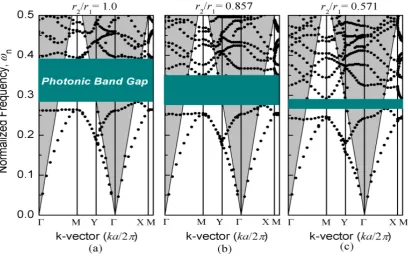
analyzing various diagrams related to the frequency structure and comparing them with each other, give the best semiconductor in its polarization for the square structure.
2. Structure of Photonic Crystal
Waveguide Sensor
It is assumed that the structure of the photonic crystal waveguide is formed in a borehole waveguide with a 3-μm span with longitudinal rotation. The refractive index of the waveguide is 2.4 and its surrounding environment
.
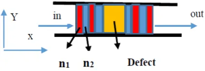
[image:3.595.70.282.382.455.2]A one-dimensional photonic crystal composed of 8 rotations on the right and 8 rotations on the left, with a defect in the middle of it. Each frequency is composed of two layers with failure coefficients of 1.32 and 1.60, and 80 and 55 nm in length. The length of the environment is 860 nm and the silica glass is impregnated with nanoparticles of gold at 25 nm. The length and refractive index of the photonic crystal components are chosen in such a way that the forbidden photonic region and the defective mode are located at the surface of the plasmon aggravation. The schematic of the structure defined in Fig. 1
.
Figure 1. Schematic design of photonic crystal waveguide
3. Designing a Photonic Crystal
Biosensor
The structure of the present crystal is formed by creating air cavities in a dielectric body made of silicon. The refractive index of air is equal to 1 and the dielectric body refractive index is 2.825. The radius of the air cavities in the structure is 90 nm and the distance between the centers of the two adjacent cavities is 360 nm. As can be seen in the figure, the defect is composed of two waveguides with closed ends and a bend and a resonator between the two waveguides. The waveguides are formed by filling the generated cavities and resonator with the decrease in the size of the cavity radius in the photonic crystal structure. At the beginning of the lower waveguide selected as input waveguide, an optical pulse source is used to stimulate the structure's resonate mode.
The light entering the structure is reached through the waveguide of the input to the resonator, and after the
resonator is stimulated, it is exerted and transmitted to the upper waveguide, which is considered as the waveguide of the output. The light transmitted by the output waveguide at the end which detected by a monitor and the output transmission spectrum.
The waveguide design in the form of a waveguide whose end is closed and also bends over its own is due to the fact that both actions on the waveguide contribute to a higher coupling of light between the waveguide and the resonator. On the other hand, a high optical limit in the structure of biological sensors is considered. This design helps the waveguides to do this. In this structure, in order to increase the optical limitation, the resonator is formed by decreasing the holes.
The distance between the waveguides and the resonator, which is called the coupling distance, is effective in the light constraint and the proper coupling between the waveguides and the resonator. By increasing the coupling distance between the waveguides and the resonator, the interaction of the biological molecule and light in the cavity is reduced. In this case, the sensor quality increased. In addition to reducing the output range and making the detection more difficult, it reduces the sensitivity of the sensor. On the other hand, by reducing the coupling distance, the interaction of light and material increases, and improves the sensitivity of the sensor and improves the intensity of the output spectrum. But the quality factor of the structure decreased.
In this structure, in order to have an optimal mode for all the effective parameters in the investigation of photonic crystal biosensors, the coupling distance is equal to two rows of air cavities between the waveguides and the resonator.
The sensing mechanism in this biodegradable sensor is based on changing the wavelength of resonance for bio-molecular bonds to the sensor cavity wall. In this structure, the middle cavity of the resonator with the highest optical interaction is considered as a measuring cavity. By connecting the biochemical molecule to the measurement cavity wall, the refractive index varies in the range of this cavity. This change in the resonator's structure causes the resonant wavelengths to shift in the output transmission range. Usually, the wavelength of the resonator is shifted to longer wavelengths.
Figure 2. Photonic band gap curve in TE and TM modes
4. FDTD Method for Photonic Crystal
Biosensors
FDTD method is a famous computational electrodynamics modeling method (Yee 1966, Taflove and
Brodwin 1975).
FDTD uses the YEE algorithm in a discrete time-dependent Maxwell equation for both E and H polarizations. Taking into account the Maxwell equations, the harmonic functions H (r, t) and E (r, t) can be written as the inverse Fourier transform in time and space, and in accordance with the Bloch theorem in solid state physics and the Brillouin Zone (BZ) [18], the main cells in the interconnected grid are obtained for polarization E and H respectively, as follows
:
𝜮𝑮𝜻�𝑮´− 𝑮��𝒌 + 𝑮´� × [(𝒌 + 𝑮)×𝑬(𝒌 + 𝑮, 𝝎)] + 𝝎𝟐
𝑪𝟐𝝐(𝑮´− 𝑮)𝑬(𝒌 + 𝑮, 𝝎) = 𝟎 (1)
Here G is the cross-grid vector and ω is the frequency. Now, with respect to the Poynting’s theorem, we use electromagnetic waves for both TE and TM modes in a two-dimensional system.
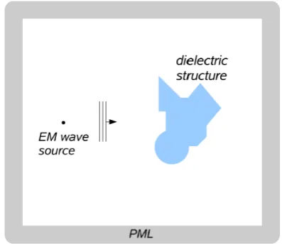
[image:4.595.65.285.81.265.2] [image:4.595.96.492.395.565.2]It is confirmed that a Yee lattice includes various square sections. Every section of a Yee lattice is taken a mean dielectric constant amount considering to the form of the geometric structure of an object. To figure out very well, let’s insert a triangular object into the Yee lattice in following Fig. 3.
The triangular structure is on six Yee lattice sections. Three of them include air and dielectric material. Considering the rule, their dielectric constant amounts are given 5. Therefore our triangular object observed in Fig. 3. With this rule, any kind of structure that we examine can be inserted in a simulation space (see Fig. 4).
Figure 4. FDTD simulation space with PML that absorbs EM waves at
simulation limits without any reflections
To obtain more actual findings, the Yee lattice must be inserted more than 18 sections. Moreover, it cannot be a various number due to computer technology limits. Before beginning a computation for a different type of structure, we must find an ideal number.
In Fig. 4 EM waves absorb at simulation limits without any reflections. It prepares us examining tiny simulation space without any reflection impacts from simulation limits. Then we obtain times during a computation.
According to Poynting’s theorem
𝑆 =𝜇10(𝐸 × 𝐵) (2) there are two possibility for that EM waves propagate in yz plane. One of them is
𝐸𝑥≠ 0 ∶ 𝐸𝑦= 𝐸𝑧= 0
𝐻𝑥= 0 ∶ 𝐻𝑦≠ 0 ∶ 𝐻𝑧≠ 0 (3) This is TE mode, due to that E is perpendicular to propagation aspect of EM wave. The other one is
𝐸𝑥 ≠ 0 ∶ 𝐸𝑦≠ 0 ∶ 𝐸𝑧≠ 0
𝐻𝑥≠ 0 ∶ 𝐻𝑦= 𝐻𝑧= 0 (4) This is TM state, so H is perpendicular to propagation aspect of EM wave. The eigenvalue equation is blocking diagonal. Therefore it can be written two independent eigenvalue equations. With
𝐴´
𝐺´𝐺= 𝜁�𝐺´− 𝐺�(𝑘 + 𝐺). (𝑘 + 𝐺´) 𝐵´
𝐺´𝐺=∈ �𝐺´− 𝐺�
𝑥´
𝐺= 𝐸𝑥(𝑘 + 𝐺, 𝜔): 𝜆 =𝜔
2
𝑐2 (5)
one of them is
𝐴´𝑥´= 𝜆𝐵´𝑥´ (6) the other eigenvalue equation is
𝐴″𝑥″= 𝜆𝐵″𝑥″ (7) where 𝐸𝑥= 0. Finally equation 7 is 2N ×2N generalized eigenvalue problem for TM states considering to Equation 4.
According to the findings we state that our frequency splitting device can separate different frequencies for TE modes. Moreover, the device behaves like a reflector for TM modes. We have applied the dimensionless frequency range 0.415 < w < 0.389. In addition our calculations are for visible light range of EM spectrum so we have given for visible spectrum.
5. Simulation
Now, by programming with Matlab code, we calculate and plot the frequency band of the important semiconductors in the electronics industry, especially the industry of producing photonic crystal biosensors in E and H polarizations in square Brillouin Zone at room temperature equivalent to 4000K. Where N is the number of flat plate waves for expansion in any direction. Considering this, we can obtain the total number of waves from equation (8)
𝑀 = (2𝑁 + 1) × (2𝑁 + 1) (8) It should be noted that in this regard we consider the value of N to be 7. So the total number of waves is 0.451. Also, for these calculations, the number of longitudinal divisions along the circumference of the irreducible zone is 10. The genus of the cavities contained in the photonic crystal biosensors used in all semiconductor materials here is composed of air and is considered to be equal to 1. To calculate these semiconductor materials in equal and identical conditions, and to obtain the appropriate results for comparing the semiconductors with each other to make the biosensors more efficient, we consider the ratio of the radius to the constant of the network to be equal to 0.435. In this way, we examine the most important semiconductors under the same conditions. These semiconductors include ZnS, Ge, CdTe, AIN, SiC, GaSb, GaAs, Si, GaN, InN, InAs, InP, InSb, AlSb, CdS, GaP, PbS, and PbTe.
In the following, we describe the results of several of the best semiconductors.
shown. According to this form, the bandwidth in the square structure of the polarization E in the range of 0.354 to 0.3598 is equals to 0.1245 and in the polarization H in the range of 0.284-0.365 is equal to 0.0223.
Figure 5. Frequency band structure for photonic crystal of Zns rods
[image:6.595.63.289.141.309.2]According to Fig. 6, in this simulation of the dielectric rods of Ge with electric permittivity 16 and radius of 0.299 for air in the square grid has been used
.
With the FDTD method, the result obtained for the bandwidth of the frequency band in the polarization E, the square grid in the range of 0.2012- 0.2154 is equal to 0.1156 and for the polarization of H in the range of 0.2203-0.2451 is equal to 0.1237.
Fig. 7 shows the band structure for CdTe rods with ∈𝑟
=12.4 and the ratio of radius to the network constant 𝑟
𝑎=0.435 is drawn
.
According to the shape of the bandwidth of the photonic crystal biosensors made from the semiconductor CdTe in polarization E, the square structure in the range of 0.2125-0.2899 is equal to 0.1032 and the bandwidth in the polarization of H, the square structure in the range of 0.2988-0.2451 is equal to 0.1125.
A photonic crystal biosensors composed of AINs with columns with a square structure with an electrical passage of 7.5 in the air is present
.
The band structure of this photonic crystal by FDTD method in polarization E in the range of 0.1899 to 0.2541 is equal to 0.1145 and in polarization H in the range of 0.2012 to 0.2456 is equal to 0.1024.Photonic crystal biosensors with air cavities inside the GaSb blade with a radius-to-constant ratio of 0.299 and an electric permeability of 1359.11 are considered
.
The band structure of this photonic crystal is shown in Fig. 9 with the FDTD method in two polarizations E and H for the square structure. The frequency bandwidth in polarization E in the range of 0.2011-0.2541 is equal to 0.1002 and in polarization H in the range of 0.2145-0.2348, and respectively is equal to 0.1022. The photonic band structure of the square grid is plotted in accordance with the ratio of the radius to the grid constant of 0.299 and the electrical permeation of the semiconductor SiC is equal to 9 in Fig 10.
Given this form, frequency bandwidth of the photon beams in polarization E in the range of 0.2145 to 0.2198 is equal to 0.1032; frequency bandwidth of the photon beams in polarization H in the range of 0.2314 to 0.2899 is equal to 0.1078.
[image:6.595.88.509.466.718.2]Figure 7. Frequency of photonic crystal biosensors bandwidth structure of CdTe rods
[image:7.595.88.512.84.362.2] [image:7.595.91.508.399.664.2]Figure 9. Frequency of photonic crystal biosensors bandwidth structure of Gasb rods
Figure 10. Frequency of photonic crystal biosensors bandwidth structure of SiC rods
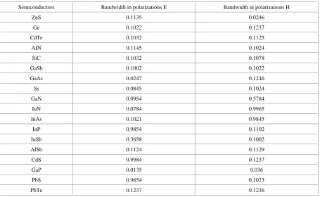
[image:8.595.159.440.363.589.2]Table 1. Bandwidth in a square structure in two polarizations E and H for photonic crystal biosensors in important semiconductors
Semiconductors Bandwidth in polarizations E Bandwidth in polarizations H
ZnS 0.1135 0.0246
Ge 0.1022 0.1237
CdTe 0.1032 0.1125
AIN 0.1145 0.1024
SiC 0.1032 0.1078
GaSb 0.1002 0.1022
GaAs 0.0247 0.1246
Si 0.0845 0.1024
GaN 0.0954 0.5784
InN 0.0784 0.9965
InAs 0.1021 0.9845
InP 0.9854 0.1102
InSb 0.3658 0.1002
AlSb 0.1124 0.1129
CdS 0.9984 0.1237
GaP 0.0135 0.036
PbS 0.9654 0.1023
PbTe 0.1237 0.1236
Here, the photonic crystal biosensors bandwidth structure of GaAs with an electrical permeability ratio of 1.13 in the air is presented. The photonic crystal biosensors bandwidth structure for calculating the GaAs bandwidth for the polarization E and H in the square structure is presented in Fig. 11, which range 0.1547 and 0.1899 and 0.2569 to 0.2348 is equal 0.0247 and 0.1246 respectively.
Figure 11. Frequency of photonic crystal biosensors bandwidth
structure of GaAs rods
6. Conclusions
In this paper, the performance of a two-dimensional photonic crystal biosensor improved with the optimization of different parameters and the FDTD method. The
photonic crystal used in the biosensor structure consists of periodic layers of ZnS, Ge, CdTe, AIN, SiC, GaSb, GaAs, Si, GaN, InN, InAs, InP, InSb, AlSb, CdS, GaP, PbS, and PbTe. In the center of this structure, a defect layer is embedded with a radial refraction distribution function. Around the central defect layer, there are two channels that allow the fluid to flow through the biological material. As a result of the presence of the central defect layer, the intensity of the light output of the circular distribution is determined by the radius of this ring depending on the refractive index of the fluid flow in the channels. Using this sensor lead to changes in the current flow failure rate in channels is detectable. The surface layer near to the channels with ligands provides the ability to analyte on the surfaces. Hence, the concentration of the analytic in the channels will be increased and the major changes in the refractive index in the channels will be due to the presence of these materials, which will lead to the selection of the sensor function. By optimizing different parameters such as channel thickness, the number of alternating layers of photonic crystal structure, as well as constant in the distribution function of the defect coefficient of the central defect, the sensor function is enhanced and the coefficients of refraction can be detected.
[image:9.595.71.527.90.370.2] [image:9.595.62.283.483.649.2]H, the square structure of the CdTe semiconductor band with a bandwidth of 0.1125 and later GaP and PbTe equivalent bandwidth are the best semiconductors for making photonic crystal biosensors.
REFERENCES
Otupiri R., Akowuah E., Haxha S., Ademgil H., [1]
AbdelMalek F., Aggoun A (2014). A novel birefrigent photonic crystal fibre surface plasmon resonance biosensor. IEEE Photon. J. 2014; 6 doi: 10.1109/JPHOT.2014.233571 6
Chakma, Sujan & Khalek, Md & Paul, Bikash Kumar & [2]
Ahmed, Kawsar & Hasan, Md. Rabiul & Bahar, Ali Newaz (2018). Gold-coated photonic crystal fiber biosensor based on surface plasmon resonance: Design and analysis. Sensing and Bio-Sensing Research. 18. 10.1016/j.sbsr.201 8.02.003
Dutta, H.S., Goyal, A.K., Pal, S (2014). Sensitivity [3]
enhancement in photonic crystal waveguide platform for refractive index sensing applications. J. Nanophoton. 8(1) (2014). doi: 10.1117/1.JNP.8.083088
Goyal, A.K., Pal, S (2015). Design and simulation of [4]
high-sensitive gas sensor using a ring-shaped photonic crystal waveguide. Phys. Scr. 90(2) (2015a). doi: 10.1088/0031-8949/90/2/025503
Zhang, Y., Han, S., Zhang, S., Liu, P., Shi, Y.: High-Q and [5]
high-sensitivity photonic crystal cavity sensor. IEEE Photon. J. 7(5), 1–6 (2015a). doi: 10.1109/JPHOT.2015.24 69131
Yang, D., Wang, C., Yuan, W., Wang, B., Yang, Y., Ji, Y [6]
(2016). Silicon on-chip side-coupled high-Q micro-cavities for the multiplexing of high sensitivity photonic crystal integrated sensors array. Opt. Commun. 374, 1–7 (2016)
R. Ahmed, A.A. Rifat, A.K. Yetisen, S.H. Yun, S. Khan, H. [7]
Butt (20146). Mode multiplexed waveguide sensor, J. Electromagn. Waves Appl. 30 (2016) 444–455
Yuan G., Gao L., Chen Y., Liu X., Wang J., Wang Z (2013). [8]
Improvement of optical sensing performances of a double-slot-waveguide-based ring resonator sensor on silicon-on-insulator platform. Optik. 2014; 125:850–854. doi: 10.1016/j.ijleo.2013
Coelho, J.M.P. Nespereira, M. Abreu, M. and Rebordão. J [9]
(2013). 3D Finite Element Model for Writing Long-Period Fiber ratings by CO2 Laser Radiation. Sensors, 13,
10333-10347; doi:10.3390/s130810333.2013
Chakma, S.; Khalek, M.A.; Paul, B.K.; Ahmed, K.; Hasan, [10]
M.R.; Bahar, A.N (2018). Gold-coated photonic crystal fiber biosensor based on surface plasmon resonance: Design and analysis. Sens. Bio-Sens. Res. 2018, 18, 7–12
A.A. Rifat, G. Mahdiraji, Y.M. Sua, R. Ahmed, Y. Shee, [11]
F.M. Adikan (2016). Highly sensitive multi-core flat fiber surface plasmon resonance refractive index sensor, Opt. Express 24 (2016) 2485–2495
Rifat, A.A.; Mahdiraji, G.A.; Sua, Y. M.; Shee, Y.G.; [12]
Ahmed, R.; Chow, D.M.; Adikan, F.M (2015). Surface Plasmon Resonance Photonic Crystal Fiber Biosensor: A Practical Sensing Approach. IEEE Photonics Technol. Lett. 2015, 27, 1628–1631
C. Ciminelli, F. Dellolio, D. Conteduca, C. M. Armeniese, [13]
“High Performance SOI microring Resonator for Biochemical Sensing”, Optics & Laser Technology, Vol. 59. Pp. 60- 67, 2014
Liu, C.; Yang, L.; Lu, X.; Liu, Q.; Wang, F.; Lv, J.; Sun, T.; [14]
Mu, H.; Chu, P (2017). Mid-infrared surface plasmon resonance sensor based on photonic crystal fibers. Opt. Express 2017, 25, 14227–14237
Z. Dorrani, M. A. Mansouri-Birjandi (2012). Superlens [15]
Biosensor with Photonic Crystals in Negative Refraction, International Journal of Computer Science Issues, Vol. 9, Issue 3, No 1, (2012), 57-60
Rifat, A.; Mahdiraji, G.; Chow, D.; Shee, Y.; Ahmed, R.; [16]
Adikan, F (2015). Photonic crystal fiber-based surface plasmon resonance sensor with selective analyte channels and graphene-silver deposited core. Sensors 2015, 15, 11499–11510
Liu, B.; Lu, Y.; Yang, X.; Yao, J (2016). Surface plasmon [17]
resonance sensor based on photonic crystal fiber filled with core-shell Ag-Au nanocomposite materials. Opt. Eng. 2016, 55, 117104
OA. Yeshchenko, IS. Bondarchuk, VS. Gurin (2013). [18]
Temperature dependence of the surface plasmon resonance in gold nanoparticles, Surface Science (2013)
C. Ciminelli, F. Dellolio, D. Conteduca, C. M. Armeniese, [19]
“High Performance SOI microring Resonator for Biochemical Sensing”, Optics & Laser Technology, Vol. 59. Pp. 60- 67, 2014
Zhou, C (2013). Theoretical analysis of [20]
double-microfluidic-channels photonic crystal fiber sensor based on silver nanowires. Opt. Commun 2013, 288, 42–46
Hirose K. et al. Watt-class high-power, high-beam-quality [21]
photonic-crystal lasers. Nat. Photon. 8, 406–411 (2014)
R. J. E. Taylor et al., "Photonic crystal surface emitting [22]
lasers based on epitaxial regrowth," 2013 Conference on Lasers and Electro-Optics Pacific Rim (CLEOPR), Kyoto, 2013, pp. 1-2. Doi: 10.1109/CLEOPR.2013.6600281
Malik Kemiche, Jérémy Lhuillier, Ségolène Callard, [23]
Christelle Monat (2018). Design optimization of a com-pact photonic crystal microcavity based on slow light and dispersion engineering for the miniaturization of integrated mode-locked lasers. AIP Advances, American Institute of Physics- AIP Publishing LLC, 2018, 8 (1), pp.15211 - 15211. <10.1063/1.5008476>. <hal-01787181
Yasutomo Ota, Ryota Katsumi, Katsuyuki Watanabe, [24]
Satoshi Iwamoto & Yasuhiko Arakawa (2018). Topological photonic crystal nanocavity laser. Communications Physics volume 1, Article number: 86 (2018)
Takashi Asano; Susumu Noda (2018). Photonic Crystal [25]
Devices in Silicon Photonics. Proceedings of the IEEE. Volume: 106, Issue: 12, Dec. 2018. Page(s): 2183 – 2195. DOI: 10.1109/JPROC.2018.2853197
Wenjun Liu, Nicolas Poilvert, Yihuang Xiong, Ismaila Dabo, Suzanne E. Mohney, John V. Badding, and Venkatraman Gopalan (2016). Single-Crystal Silicon Optical Fiber by Direct Laser Crystallization. ACS Photonics, 2017, 4 (1), pp 85–92. DOI: 10.1021/acsphotonics.6b00584
Hongtao Lin, Zhengqian Luo, Tian Gu, Lionel C. Kimerling, [27]
Kazumi Wada, Anu Agarwal and Juejun Hu (2018).Mid-infrared integrated photonics on silicon: a perspective. Nanophotonics 2018; 7(2): 393–420
Yasutomo Ota, Katsuyuki Watanabe, Masahiro Kakuda, [28]
Nonmembers, Satoshi Iwamoto, Member, and Yasuhiko Arakawa(2018).IEICE TRANS. ELECTRON., VOL.E101–C, NO.7 JULY 2018
Goyal, A.K., Dutta, H.S. & Pal, S (2016). Performance [29]
optimization of photonic crystal resonator based sensor. Opt Quant Electron (2016) 48: 431. https://doi.org/10.1007/s11 082-016-0701-0
Rifat, A. A., Mahdiraji, G. A., Chow, D. M., Shee, Y. G., [30]
Ahmed, R., & Adikan, F. R. (2015). Photonic crystal fiber-based surface plasmon resonance sensor with selective analyte channels and graphene-silver deposited core. Sensors (Basel, Switzerland), 15(5), 11499–11510.
X. Chen, L. Xia and C. Li (2018). "Surface Plasmon [31]
Resonance Sensor Based on a Novel D-Shaped Photonic Crystal Fiber for Low Refractive Index Detection," in IEEE Photonics Journal, vol. 10, no. 1, pp. 1-9, Feb. 2018, Art no. 6800709
Xudong Li, Shuguang Li, Xin Yan, Dongming Sun, Zheng [32]