Ifaskop
Technical Description
E90003062E-3 1984-12-14
Text Section
E less
(Jeneral Concepts I. EE355-XIOD Microcomputer 2. EE3S6-XI0D Communication 3. E90002331 E-I Communication Processor, 4. Remote, CPR 4101
EE358-8108
Communication Processor, 5. Local, CPL4102
E90002332E
Communication Processor, 6. Remote, CPR4103
E90002659E Flexible Disk Unit, 7. FD4120
EE369-810 Flexible Disk Unit, 8. FD4122
E90002914E Display Unit, 9. DU4110
EE360-810C Display Units, 10. DU 4111 and DU 4112
E90002943E-l Display Unit, 11. DU4113
E90003450E Work Station, 12. WS3111
E90003218E
Keyboard, KBU 4140, 13. KXU4141
EE361-810
Keyboard, KBU 4143, 14. KXU 4146, MSR4136
E90003341E
Magnetic Identification 15. Device, MID 4131
EE362-810
Selector Pen Device, 16. SPD4130
EE363-810
Peripheral Control Unit, 17. PCU 4171
E90003284E 18.
Synchronous Communication 19. Adapter, SeA 4194
EE364-810
Synd. canous Communication 20. Controller, SCC4195
EE365-810
Asynchronous Communication 21. Adapters, ACA 4185M193/4199
EE366-810B
Memorv Board R/W,
22. Iv!RW 4191 EE367-81O
Memory Board RO, 23. MR04192
This is the text section of the Technical Description for Alfaskop System 41. Its objective is to describe the main functions carried out by the logic of the display units, the flexible disk units and the communication processors as realized by the printed circuit boards.
Chapter 1 serves as general information on the system. Functions or circuits common for two or more units are described in chapter 2 and 3. The other chapters deal with specific units or logic boards.
Certain information is quoted from Motorola Inc. publications.
For information on printers and flexible disk drives, please refer to separate documents. Titles and Printed matter numbers can be found in the Service Infor-mation binder under Index of Current Literature.
Tips for the reader:
• A byte consists of eight bits if nothing else is said.
• Bit 0 always designates the least significant bit of a word. E.g. bit 7 (for data) or bit 15 (for addresses) is the most significant bit. Bit is often written b, e.g. b7 means bit 7.
• X or - in register descriptions normally means don't care bits.
• A pin of an integrated circuit or of a connector and sometimes a bit in a register is indicated as a number after a colon. E.g. pin 12 of IC25 will be written as 25:12, pin 2 of connector P1 could be indicated as P1 :2.
• A bar over a signal name or a circle on a drawing of a wire or before a signal name indicates that low level is active (or negative logic for buses). E.g. °Bus addressing means that addressing from bus takes place when the signal °Bus addressing is low.
The specifications in this publication are subject to change and supplementation without notice.
It is possible that this manual contains information on Alfaskop products or functions
no longer or not yet available in your country. This shall not be construed to mean that an announcement of such Alfaskop products or functions will be made in your country.
This is a revised edition of publication E90003062£-2. A new chapter Display Unit, DU 4113, has been added. The chapters 7, 9, 13, 15 - 16, 19 - 20 and 22 - 23 will be updated as soon as possible but until then, some of the references to the Microcomputer chapter are actually found in the Communication or Power Supplies chapters. ©1984, Ericsson Information Systems AB,
Data Terminals Documentation
S-175 86 larfalla, Sweden
)
(
(
ERICSSON ~
Reader comments
You can help improve future editions of this document by answering the following questions and sending us your comments.
1. Document name and number:
-2.
~yjob:---3. I have used this document
o
To acquire general information (for-o
As a technical manual (reference book)o
As a textbook in a course (trainee)o
As source material for teaching a course (instructor)Comments:
-4. I think this document is
o
Easy to find things ino
Easy to find things in with some reservationso
Difficult to find things inC o m m e n t s :
-5. I think this document is
o
Easy to understando
Easy to understand with some reservationso
Difficult to understandC o m m e n t s :
-6. I think this document is
o
Well illustratedo
Poorly illustratedComments:
-7. I think that this document provides
o
FuB coverage of the subject at hando
Poor coverage (essential parts are lacking)-8. I think that this document is
o
Well adapted to my skills and knowledgeo
Poorly adapted to my skills and knowledgeComments:
9. Other comments:
-We appreciate your cooperation.
Please send your answers and comments to
Ericsson Information Systems AB· Alfaskop
Documentation Department
S-175 86 Jarfalla, Sweden
(
(
ERICSSON
ili
IGeneral Concepts
Contents
Introduction _ _ _ _ _ _ _ _ _ _ _ _ _ _ _ _ _ _ _ _ _ _ 1 System Architecture _ _ _ _ _ _ _ _ _ _ _ _ _ _ _ _ _ _ _ _ 1
Some Configuration Examples 1
(
ERICSSON
:s
General ConceptsIntroduction
This chapter contains a brief presentation of the hardware components of Alfaskop System 41. For detailed information on combination possibilities for different emulations (IBM 3270, UTS 400 etc.) look in the respective reference manual.
System Architecture
Some Configuration Examples
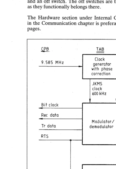
Fig. 1 shows a single display unit connected to a computer via modem and telephone lines (remote connection). Descriptions of modem interface logic boards are found in the SCA and ACA chapters.
Display Unit 4110 with Keyboard Unit 4140 and Keyboard Expansion Unit 4141
Flexible Disk Unit 4120
Fig. J. Example of single display unit configuration
Host computer
Printer Unit 4153
Host computer Communication _1111'1111111111 ~1IIIlI!JIIJIIII
)
Modem
I--z.-Flexible Disk Unit 4120
Processor 4101
-J
Max3 peripherals _on same _ _
Display Unit 4110 with Keyboard Unit 4140 and Keyboard LSi~n Unit 4141 •
2-wire connec-tion
Printer Unit 4153
Work station
Flexible Disk Unit 4120
l
Printer Unit 4154Display Unit 4110 with Keyboard Unit 4140 and Keyboard Expansion Unit 4141
(V.24/28)
Fig. 2. Example a/terminal cluster connected remotely to host computer
Fig. 2 shows an example of a cluster configuration (more than one terminal using the same line to communicate with a computer). The communication processor communicates with display units and flexible disk units via two-wire cables. The printers are connected to display units via V24/V28 cables.
~)
tr1 tr1 y..) Vl Vl I 00 i-" o
o
:!! ~Cl ~ V:l~
~. {g' ~ ~ ~, 8 S, OQ' ~ ~ 6' ;::: ~ §. ~ ~ .)To modem " I I I
Printer Unit 4153/54
Display Unit 4110
,~
Flexible Disk Unit 4120
Keyboard Unit 4140
Selector Pen Device 4130
Keyboard Expansion Unit 4141
J
r I Magnetic Identification Device ,4131 ~qQ'
v.J rJl ::r 0 ~ rJl rJl 03
(t) 0 to-o!-):;.
(t) (') 03
'"d 0 t::J (t)a
rJl 0 I-t-, cs,
... rJl C rJl (t) 0.. 5' rJl 5' a.s.. (t)Fig. 4 shows the components of units used in remote cluster configurations. Note that a communication processor for remote connection to a host computer (CPR) is shown.
0 "<t :; 'c ::> '0 ro 0 .0 >-Q) x: 0 ~
~
~ / / , / / / / ID U .:;: ID Cl Co IDe')0...-... '<1'
0 tl ID Qi (/J ~ ~I ~I
II
~I 'E jJ ~ ::;;: 'c ::l >-ctI0.. <Jl 0
~ -g
E . 0 I- ::-0 E ~ ~
'C '5
c CD
<0
~.~
«
:i:
0 11.'0 0
:: C\I
.~ ::;;:
Q; 'c
0.. CD ::l
<0<>
-"
'COl <Jl
<o't:
0
",CD
:5£ ID
CD~ ~N :c
r~ 0c::i 'x ID
£~ CD~ .U::
;e!
x>
~''::
u..O
Fig. 4 Remote cluster configuration details
)
t11 t11 w Vt Vt I 00 ~ o tj
?
VJ t--' o C"l ~ C"l ~ ~ ""I C"l o S, OQ' :::: ~ ~. ;:s f} §. ~CJ-
I
-U'""
"-Printer Unit 4153/54
Channel communication controller
Microprocessor
[ . Memory
[ Memory , expansion
Communication Processor 4102
/...,..."
~)
"'-"'-"
"
'u , .-,~rd~a~n ~du.!!0d Display Unit 4110
Flexible Disk Unit 4120
,.----v
Keyboard Unit4140 ~
Selector Pen Device
J
4130 m :an
""
""
0 z !1 \\\ Keyboard ExpansionI
(Jq Unit4141 Vl rn =r' 0I
~1
'/
I
rn f""t-=r'
(l)
(')
Magnetic Identification 0
Device 4131
3
~
0
~ (l) C)
:::I n.
f""t- ;:s
rn I'1l
0 ""I ~
r-+-,
g
s:::
2. ;:s C"l
r-I-~ rn
s::: E:; (/) (l) 0-S· ..-. 0 (') ~ ..-. 0.. s::: (/) f""t-(l) ""'t (') 0 ~ t:h (Jq s::: ""'t ~
f""t-o·
~Abbreviation List
ACA BXM CCC CIB CP CPB CPL CPR CPS CRU CTF DPS DTC DU FD FDA FDD FDPFPS
KB KBC KBU KXB KXU MIA MID MRO MRW PTC PU SeA SCC SPA SPD TAB TIA TUA UPSAsynchronous communication adapter
Board expansion module
Channel communication controller CCC interconnection board
Communication processor
= CPboard
CP, local CP,remote
=. CPpowersupply
Cathode ray tube unit CP and tenninal fan
Display terminal power supply Display terminal controller Display unit
=
Flexible disk unit Flexible disk adapter Flexible disk drive=
Flexible disk processor Flexible disk power supplyKeyboard
Keyboard controller Keyboard unit
=
Keyboard expansion boardKeyboard expansion unit
MID adapter
Magnetic identification device Memory board, RO memory
=
Memory board, RlWmemory=
Printer terminal controller Printer unitSynchronous communication adapter Synchronous communication controUer Selector pen adapter
= Selector pen device
TU A interconnection board
= Two-wire interface adapter
Terminal unit adapter
=
Universal power supply(
( ~\
ERICSSON ;! I
Microcomputer
Contents
General __ ~ _____________________________________________ ___ 1
Microprocessor Unit, MPU __________________________________ _ 2 2
4 5
MPU Registers ____________________________________ _ MPU Signals ______________________________________ _ Instruction Set and Addressing Modes
Interrupt Handling 8
General 8
Address Modifier ___________________________________ 10
Mask Register 10
Interrupt Register 10
Generation and Direction of IRQs 10
Interrupt Priority and Address modifier (FPLA) 11
Peripheral Interface Adapter, PIA 12
Signals 12
Registers 13
Timing ____________________________________________ 16 Basic Timing _______________________________________ 16
Bus Timing Example 16
Programmable Timer Module, PTM 16
Signals 18
Registers 19
Memory Organization and Access ______________________ 21
Memory Map 21
Address Decoding and Direct Memory Access 23
Address Decoder (FPLA) 23
Memory Access Multiplexing 23
Direct Memory Access 24
Direct Memory Access Controller, DMAC 25
DMAC Programming Example 27
(
(
(
ERICSSON ~ Microcomputer 1
General
All main units of Alfaskop System 41 include ~ microcomputer. The purpose of this chapter is to describe the common attributes of the differ<ent M6800 family based microcomputers. Thus e.g. the most common LSI circuits of the M6800 family, the bus system, the addressing modes, the interrupt handling and the employed direct memory access method are described in this chapter. Even more detailed information on the M6800 family can be found in Motorola Semiconductors: Microcomputer components.
This chapter is directly applicable for the microcomputers in DU 4110, CPR 4101, CFU 4103 , and in the communication processor parts of CPL 4102. (The reader ought also to be familiar with this chapter before studying the chapter on FD 4120.) The main functional blocks of the microcomputer are shown in Fig. 1.
'toe--+-+---li
:::>
0-4
..
;
~ 14---+-+---'
\ - - - ' QJ
~~--~ ~
Fig. 1. Microcomputer, basic block diagram
VI (:':b' ~ ~
4 ~
These are:
• Microprocessing unit, MPU
• Timing logic
• Memory
• Address decode, bus timing and parts of memory access multiplexing logic
• Interrupt control logic
• IPL ROM, i.e. a read only memory containing the necessary program for initial program loading
The microprocessing unit used is of the M6800 type or similar, thus with an 8-bit data bus and a 16-bit address bus. No specific I/O instructions are used, but registers of peripheral circuits like parallel interface and serial interface adapters are addressed just as memory locations. The MPU is described in detail below.
Microprocessing Unit, MPU
In this paragraph the hardware and software attributes of the MPU are dealt with. The MPU is an 8-bit parallel three-state device. It has 16 address bits and is thus capable of addressing 65,536 memory locations. See Fig. 2.
Processor Control
r "=--
_--=-...:::-~-DBE TSC SA HAlT NMI Reset
.
F-~---~
Accumulator A
I
Accumulator BIndex register
stack po inter
Program cau nter
CCR=
I
HII IN I Zl
VJ (
.
16- bit address
bus
Bus
(ontrol
Fig. 2. MPU registers and signals
MPU Registers
+ SV (/)2 Reset.,
Seen from the outside, the MPU contains six registers; three one byte registers and three double byte registers. The one byte registers are:
~ Two accumulators named ACCA and ACCB used for storing operands
for and results from operations.
)
(
ERICSSON ;i Microcomputer 3
• A condition code register, CCR, with 6 flag bits (b7 and b6 are always ones) signalling the result of a previous operation. The meaning of the different CCR bits, when set, are:
b5 H A preceding operation (e.g. ADD, SUB, CMP) resulted in a half-carry from bit 3 to bit 4.
4 I When this bit is reset, the MPU will service a maskable interrupt request (IRQ). It will be set when an interrupt occurs, thus hindering or "masking" further interrupts (IRQs). 3 N The result of a preceding operation is negative (bit 7 of
result
=
1).2 Z The result of a preceding operation
=
o.
1 V A previous operation resulted in 2's complement overflow, i.e. a limit of the number area [- 128, 127] was passed.
o
C· A carry from bit 7 was produced by a preceding operation or a borrow to bit 7 was needed to make the operation (SUB orCMP).Detailed information on which CCR bits that are affected by a certain instruction is found in Fig. 4.
The 16-bit double registers, mostly used for addressing, are:
• Index register, which reduces program memory requirements as it can be loaded with a different memory addre~s from the one contained in the program counter and stack pointer (see addressing modes below) • Stack pointer, which should be initialized to point to the highest address of the read/write memory area to which the stack function has been assigned. At a Push data instruction (PSH) the contents of one of the accumulators (A or B) is stored in the stack and the stack pointer is automatically decremented. When data from the stack is wanted back to an accumulator a Pull data instruction (PUL) is used, reSUlting in an automatic incrementation of the stack pointer and a following loading of an accumulator from the memory cell pointed out by the stack pointer. The stack thus functions as a LIFO (last-in, first-out memory). The stack pointer is also automatically used at interrupts and at Jump to subroutine (JSR) and Branch to subroutine (BSR) instructions. In the interrupt case the contents of the MPU registers (but the stack pointer) are pushed into the stack and brought back at the Return from interrupt instruction (RTI). At JSR and BSR only the value of the program counter (i.e. the return address) is stacked away and brought back at the Return from subroutine instruction (RTS).
MPU Signals
Apart from the 16 address bus lines and the 8 bidirectional data bus lines there are several other timing and control signals in the system. The clock inputs to the MPU are:
• 01 and 02, complementary, non-overlapping clocks. The cycle time mentioned in this text is the clock cycle time. During 01 high time the address is set up and during 02 high time data is set up and read or written. (On 02 going low.) See Timing paragraph for details.
Normal program execution can be stopped by four external signals, namely Interrupt request (IRQ), Non-maskable interrupt (NMI), Reset (R) and HALT .
.. IRQ input being low will make the processor jump to an interrupt
routine if the interrupt nlask bit (I) in the MPU condition code register
is reset.
• NMI input going low will always make the MPU jump to an interrupt routine after the present instruction has been completed.
An incoming intetrupt (IRQ, NMI or Software interrupt instruction) or Reset will set the I-bit to prevent further interrupts (IRQs) from interfering with the execution of the interrupt routine.
• Reset being low win make the processor stop (if it has started). When Reset goes high again the MPU will fetch the address of the restart
routine from the two highest memory positions (FFFE(16) and FFFF (16),
load this address into the program counter and begin the restart sequence. The interrupt mask bit in the CCR will be set during Reset and nlust be cleared by the program if service of an IRQ is wanted.
• HALT being low will stop all program execution. Interrupts coming during HALT condition will be preserved and serviced after HALT
has gone high again. If Reset is low during HALT condition, the" restart
routine will be entered when HALT goes high again. The MPU will signal that it is halted with a BA signal (see below).
• BA, Bus available, is high when the MPU is halted. BA is also high when the MPU is waiting for an interrupt as a result of a Wait for
interrupt instruction. The address and the data bus as well as the RIW
signal (see below) are then in high impedance state.
• RIW, ReadlWrite, signals the peripherals and memories whether the
MPU is in read (high) or write (low) state. R/W is in high impedance
state when the MPU is halted and its buses are available for another device (e.g. another MPU) to access the memories of the system (DMA, direct memory access).
• VMA, Valid memory address, is low or non-active during HALT. This signal is active only during the cycles when the memory address from the MPU should select a specific circuit.
e TSC, Three-state control, being high puts the RIW and address bus
lines into high impedance state. The clocks for the MPU, 01 and
02, should be stopped to prevent false program execution. 01 should
be held high.
• DBE, Data bus enable, which is generally tied to 02, low, puts the data bus input/output in high impedance state (allowing DMA).
(
(
ERICSSON ~ Microcomputer
The drawing symbol is shown in Fig. 3.
Me
6800
CPU
8~
7...ol ...
01
...aIIioi~02
...,.;~::lI
R
*
...
~D8E... 1IIooCI
H
~LT
...
~TSCVM~
R/W
~O
~1
~2 ~3 ~4 ~5
-""'--""IRQ
...olllio.{"]l N M I
~
6~7
---~OO ~8
--oIIIioiI ...
Ol
~9... 02
~1003 ~ ~11
... 04
~12---... 05
~13---406
~14...-.,;~D7
...
__
... ~15Fig. 3. CPU drawing symbol
Instruction Set and Addressing Modes
5
The instruction set is shown in Fig. 4. The seven addressing modes mentioned in the headings of the instruction set are described below:
• Immediate addressing or zero-level addressing. In this case one operand is found in the memory cell (two cells for index register and stack manipulations) immediately following the operation code location. • Direct and extended addressing or one-level addressing. In these modes the operand or the operation code of the next instruction at a jump instruction is found in the cell pointed out by the byte (for direct addressing) or 2 bytes (for extended addressing) following the operation code. Thus, with extended addressing it is possible to reach cells 0000(16) through FFFF(16) but with direct addressing only cells
o
through 255 in the memory map.• Indexed addressing. In this case the effective address of the operand location is formed by adding an offset from 0 to 255 (contained in the second byte of the instruction) to the 16-bit address contained in the index register.
ACCUMULATOR AND MEMORY INSTRUCTIONS
ADDRESSING MODES
IMMED DIRECT INDEX EXTND
OPERATIONS MNEMONIC OP
-
- OP , = OP ,= OP
-
:= Add ADDA 38 2 2 98 3 2 AB 5 2 BB 4 3 ADDB CB 2 2 DB 3 2 EB 5 2 FB 4 3Add Acrnltrs ABA
Add with Carry ADCA 89 2 2 99 3 2 A9 5 2 89 4 3 ADCB C9 2 2 09 3 2 E9 5 2 F9 4 3
And ANDA 84 2 2 94 3 2 A4 5 2 B4 4 3 ANDB C4 2 2 04 3 2 E4 5 2 F4 4 3 Bit Test BITA 85 2 2 95 3 2 A5 5 2 B5 4 3 BITB C5 2 2 05 3 2 E5 5 2 F5 4 3
CIllar CLR 6F 7 2 7F 6 3 CLRA
CLRB
Comparll CMPA 81 2 2 91 3 2 Al 5 2 Bl 4 3
CMPB Cl 2 2 01 3 2 El 5 2 Fl 4 3
Compare Acmltrs CBA
Complemellt,l's COM 63 7 2 73 6 3
COMA
COMB
Compleillellt,2's NEG 60 7 2 70 6 3
INegatel NEGA NEGB Decimal Adlust, A DAA
Decremellt DEC 6A 7 2 7A 6 3
DECA
OECB
Exclusive OR EORA 88 2 2 98 3 2 A8 5 2 B8 4 3 EORB C8 2 2 08 3 2 E8 5 2 F8 4 3 Incremellt INC 6C 7 2 7C 6 3
INCA INCB
Load Acmltr LOAA 86 2 2 96 3 . 2 A6 5 2 86 4 3 LDAB C6 2 2 06 3 2 E,6 5 2 F6 4 3 Or,lllciusive DRAA 8A 2 2 9A 3 2 AA 5 2 BA 4 3 DRAB CA 2 2 DA 3 2 EA 5 2 FA 4 3
Push Data PSHA PSHB Pull Data PULA PULB
Rotate Left ROL 69 7 2 79 6 3 ROLA
ROLB
Rotate Right ROR 66 7 2 76 6 3
RDRA
RORB
Shift Left, Arithmetic ASL 68 7 2 78 6 3
AS LA
ASLB
Shift Right, ArithmetiC ASR 61 7 2 17 6 3
ASRA
ASRB
Shift Right, Logic LSR 64 7 2 74 6 3 LSRA
LSRB
Store Acmltr. STAA 97 4 2 A7 6 2 B7 5 3 STAB 07 4 2 E7 6 2 Fl 5 3 Subtract SUBA 80 2 2 90 3 2 AD 5 2 BO 4 3
SUBB CO 2 2 DO 3 2 EO 5 2 FO 4 3
Subtract Acmltrs, SBA
Subtr, with Carry SBCA 82 2 2 92 3 2 A2 5 2 B2 4 3
S8CB C2 2 2 02 3 2 E2 5 2 F2 4 3 Trallsfer Acmltrs TAB
TBA
Test, Zero or Minus TST 60 7 2 70 6 3 TSTA
TSTB
LEGEND;
OP Operalioo Code (Hexadecimal); + Boolean Inclusive OR; Number of MPU Cycles; G Boolean ExclUSive 0 R; Number of Program Bytes; M Complement of M; Arithmetic Plus; Transfer Into; Arithmetic Minus; Bit Zero; Boolean AND; 00 Byte Zero;
MSp Conlents of memory location pointed to be Slack Poinler;
Note - Accumulator addressing mode instructions are included ,n Ihe column for IMPLIED addressing
IMPLIED
OP
-
""lB 2 1
4F 2 1
5F 2 1
11 2 1
43 2 1
53 2 1 40 2 1
50 2 1
19 2 1
4A 2 1 5A 2 1
4C 2 1
5C 2 1
36 4 1
37 4 1
32 4 1
33 4 1
49 2 1
59 2 1 46 2 1
56 2 1
48 2 1
58 2 1
47 2 1
57 2 1
44 2 1
54 2 1
10 2 1
16 2 1
17 2 1 40 2 1 50 2 1
BOOLEAN/ARITHMETIC OPERATION COND CODE REG
(All register labels refer to contents)
A'M -A
B + M - B A+B -A
A+M+C -A B+M+C -B A- M -A
B - M - B
A-M
B - M 00 - M 00 -A 00 . B A M B M A B M -M A -A B -B 00 M 'M 00·· A,-A 00 8 • B
Converts Bmary Add. of B CD Characters IOta flCD Format
M 1 -M A ·1 '-A B 1- B
A<±>M "A
B0M'-B
M + 1 --M A + l ' A B + 1 • B M '-A M -8 A+ M- A B + M -- B
A" MSp, SP 1 '~SP
B' MSp, SP - 1 .• SP
SP + 1 -SP, MSP"A SP + 1~ SP, MSp - 8
~} L{] -
DIIIIID=J
B C b7 - bO~}
CO - o:o:rro::!=lB C b7 - bO
-n
0 - DIIIIIIJ- 0C b7 bO
M}~
A - 0
B b7 bO C
n
Q-OIIIIOJ - - 0b7 bO C A 'M
B 'M A M 'A B M • B A B'A
A M - C ·'A B ... M C·, B
A .• B
B-A M- 00
A 00 B - 00
CONDITION CODE SYMBOLS;
Half,carry from bit 3; Interrupt mask Negative Isign bitl Zero (byte) V Overflow, 2's complement
Carry from bit 7
Reset Always Set Always
5 4 3 2 1 0
H I N Z V C
.. ! ! : : ! .. ! !
!
..
! ! ! !; III : ! 1 !
: '" ! ! : !
"
..
! j R III....
1 : R G.. III i 1 R
..
eo .. 1 I R
..
.... R S R R
·
.. R S R R .. .. R S R R III • I ! I ! .. .. i I 1 r..
..
r 1 ! 1 III .. 1 i R S ...
I I R S..
.. ! I R S..
.
I !CDCl)·
.. I ICDc.D....
1 ICD(!J....
! 1 IG)·
.
! ! 4..
· .
r I 4..
.. .. r ! 4 \III..
.
1 ! R III \III III I I R..
.. " i !@" III • I !@. .. III I I@ ..III • 1 ! R
..
..
.. : r R..
..
..
I I R..
III '" 1 i R '" .. • III.
.. .. ....
..
.. .. GO.. ..
..
.. \III .. " .. III .." III
"
.
i I@! " .. I l@!'" It 1 li~l III '" ! !@! G III 1 !@!
'" .. I li~ I
'" 0 I I@I
'" «I I 111: !
.. I) I li~ 1 .. " I !@l
o .. ! li~ I
\III 0 ! ! 11; I
.. 0 R l@l
.. 0 R lliG'1
o .. R ll~ !
o .. i i R
..
GO 0 1 I R III
o 0 I I I I
<II <II 1 I ! I
.. 0 1 I I !
o .. ! I ! I
" " ! I 1 !
..
..
! ! R..
....
I ! R 0o " I : R R III " i I R R GO " ! ! R R
H I N Z V C
Test and set" true, cleared otherWise
Not Affected
@
MOTOROLA Se..,;conductor Products Inc.Fig_ 4a Instruction set
ERICSSON
i!E
Microcomputer 7INDEX REGISTER AND STACK MANIPULATION INSTRUCTIONS
CONDo CODE REG.
IMMEO DIRECT INDEX EXTND IMPLIED 5 4 3 2 1 0
POINTER OPERATIONS MNEMONIC OP
-
:: OP-
::: OP-
::: OP-
::: OP-
::: BOOLEAN/ARITHMETIC OPERATION H I N Z V CCo mpare I ndex Reg CPX ac 3 3 9C 4 2 AC 6 2 BC 5 3 XH-M.XL-(M+l)
·
.
(j): ®.Decrement Index Reg OEX 09 4 1 X-l-X • • • !
·
.
Decrement Stack Pntr DES 34 4 1 SP - 1 -SP
·
.
.
·
.
:1
Increment Index Reg INX 08 4 1 X + I-X
·
. .
i·
I
Increment Stack Pntr INS 31 4 1 SP + 1 -. SP
·
.
·
.
.
OIl: Load Index Reg lOX CE 3 3 DE 4 2 EE 6 2 FE 5 3 M-XH. (M + 1) ··XL • • ®! R.,
Load Stack Pntr lOS 8E 3 3 9E 4 2 AE 6 2 BE 5 3 M -SPH, (M + ll-SPL
·
.
®: R·
Store I nde. Reg STX OF 5 2 EF 7 2 FF 6 3 XH-M,X c ··IM+1i
·
.
®: R·
Store Stack Pntr STS 9F 5 2 AF 7 2 BF 6 3 SPH - M, SPL .+ (M + 1)
· .
®: R •Indx Reg - Stack Pntr TXS 35 4 1 X-I -SP
·
. ·
.
·
..
Stack Pntr - Indx Reg TSX 30 4 1 SP + 1 - X
·
.
·
.
·
..
JUMP AND BRANCH INSTRUCTIONS
CONDo CODE REG.
RELATIVE INDEX EXTNO IMPLIED 5 4 3 2 1 0
OPERATIONS MNEMONIC OP
-
# OP-
# OP-
:# OP-
# BRANCH TEST H I N Z V CBranch Always BRA 20 4 ? None • • • • •
·
Branch If Carry Clear BCC 24 4 2 C=O
·
•· ·
·
•Branch II Carry Set BCS 25 4 2 C=1
·
• • • •·
Branch If = Zero BEQ 2; 4 2 Z=1 • •
· ·
• •Branch II ;;, Zero BGE 2C 4 2 N <±l V= 0
·
• • • •·
Branch If > Zero BGT 2E 4 2 Z + (N <±l V) = 0
· · ·
•·
•Branch If Higher BHI 22 4 2 C+Z=O • • • • •
·
Branch II ,.;; Zero BlE 2F 4 2 Z + (N <±l V) = 1
·
• • • • •Branch If lower Or Same BlS 23 4 2 C + Z = 1
·
• • • •·
Branch If < Zero BlT 20 4 2 N <±l V = 1
·
•·
• • •Branch If Minus BMI 2B 4 2 N=1 •
·
•·
• •Branch If Not Equal Zero BNE 26 4 2 Z=O •
·
• • • •Branch If Overflow Clear BVC 28 4 2 V=O
·
•·
·
• •Branch If Overflow Set BVS 29 4 2 V=1 • •
·
•·
•Branch If Plus BPl 2A 4 2 N=O • • • • • •
Branch To Subroutine BSR 80 8 2 • •
·
·
• •Jump JMP 6E 4 2 7E 3 3
·
•· ·
•·
Jump. To Subroutine JSR AD 8 2 BO 9 3
· · ·
·
·
·
No Operation NOP 01 2 1 Advances Prog. Cnlr. Only
·
•· · ·
•Return From Interrupt RTI 3B 10 1 @
-Return From Subroutine RTS 39 5 1
llllT
Software Interrupt SWI 3F 12 1 ..
.
. .
. .
Wait for Interrupt* WAI 3E 9 1 • @ • • • •
nd u in the three·state mode while VMA is held I
WAI puts Address Bus, RIW. a Data B s ow.
(
CONDITION CODE REGISTER MANIPULATION INSTRUCTIONS
( .,\ CONDo CODE REG.
IMPLIED 5 4 3 2 1 0
OPERATIONS MNEMONIC OP
-
::: BOOLEAN OPERATION H I N Z V CClear Carry ClC OC 2 1 O-+C • • • •
..
RClear Interrupt Mask Cli OE 2 1 0"'1
..
R·
•·
·
Clear Overflow CLV OA 2 1 O-+V
·
•·
·
R·
Set Carry SEC 00 2 1 I"'C • • • • • S
Set In terru pt Mask SEI OF 2 1 1-1 • S
· · · ·
Set Overflow SEV DB 2 1 l"'V • •
·
..
S·
Acmltr A-+CCR TAP 06 2 1 A"'CCR @
-CCR -+Acmltr A TPA 07 2 1 CCR -+A ·1·1·,·1·1·
CONDITION CODE REGISTER NOTES: (Bit set if test is true and cleared otherwise)
(Bit V) Test: Result = 10000000? (Bit N) Test: Sign bit of most significant (MS) byte = 1?
(Bit C) Test: Result = OOOOOOOO? (Bit V) Test: 2's complement overflow from subtraction of MS bytes? (Bit C) Test: Decimal value of most significant B CD Character greater than nine? (Bit N) Test: Result less than zero? (Bit 15 = 1)
(Not cleared if previously set.) 10 (All) load Condition Code Register from Stack. (See Special Operations)
(Bit V) Test: Operand: 10000000 prior to execution? 11 (Bit I) Set when interrupt occurs. If previously set, a Non·Maskable (Bit V) Test: Operand = 01111111 prior to execution? Interrupt is required to exit the wait state.
(Bit V) Test: Set equal to result of N<±lC after shift has occurred. 12 (All) Set according to the contents of Accumulator A.
@
MOTOROLA Se ... iconduc1:or Products Inc.Example:
Branch instr. code Relative address
Contents Consecutive values (hex)
of cells of program counter
~ 37FO
1---="20""(-16-))---1 ~ 37Fl
1---0_2_~(I_6)---I ~
37F2]~ 37F5
=
(37F3+
02)' - - - '
• Implied and accumulator addressing. The instructions using these addressing modes are one byte instructions, where the operand or operands are understood from or contained in the operation code. Mostly these are instructions affecting only one or two MPU registers. For the Push data (PSH), Pull data (PUL), return (RT!, RTS), Software interrupt (SWI), and Wait for interrupt (WAI) instructions, however, memory locations indicated by the stack pointer are also affected. The No operation (NOP) instruction is special in that it only advances the program counter one step and introduces a delay of two MPU cycles before active program execution is resumed.
Interrupt Handling
General
Please refer to Fig. 1.
The MPU only reacts to four interrupts (Reset, Non-maskable interrupt, Software interrupt and Interrupt request, see Fig. 5). More interrupts are wanted and an interrupt logic is therefore contained in the microcomputer. This logic permits eight interrupts to use the IRQ line to the MPU.
In addition to the possibility to mask all IRQs by setting the I-bit of the MPU condition code register (CCR) , the MPU can set a value between
o
and 7 in a mask register to prevent IRQs below the handeled level from interrupting the program execution. IRQ 7 is the highest priority interrupt and IRQ 0 the lowest. Thus, if e.g. the mask register is set to 5, only interrupts on level 5, 6 or 7 will activate the IRQ line to the MPU.The MPU reacts to an IRQ (if the I-bit is reset) by:
I) Completing the execution of the present instruction and stepping the
program counter to point to the next instruction
• Saving the contents of its registers in the stack (contents of program counter
=
return address , etc)• Trying to fetch the address to the interrupt routine from the memory cells FFF8(16) and FFF9(16)
• Setting the interrupt mask bit of the CCR to disable further IRQs.
(
('
ERICSSON
i5
Microcomputer 9n + 1
When returning from an interrupt routine (by the RTI instruction) the registers of the MPU get their old contents back from the stack. Thus the execution of the interrupted program is resumed. Note that the I-bit value is 0, i.e. not changed when stored in the stack.
PROGRAM flOW fOR INTERRUPTS
Software Interrupt
Main Program
SWI
SP -+
c::::>
HDWR
INT
FFF8 FFF9
m - 7 m - 6
m - 5 m - 4 m - 3 m - 2 m - ,
m
No
I nterrupt Memory Assignment 1 Constant, Hdware Constant, HdWllre Software
MS
lS
MS
Hardware Interrupt or Non· Maskable Interrupt (NM II
Main Program
Stack
Condition Code Acmltr. B
Acmltr. A
Index Register IXHI
Index Register IX II
PC(n + 1)H PC(n+1)L FfF8 FFF9 FFFA FFFB FFFC FFFD FFFE FFFF Software Non·Maskable Int.
lS ~
MS~
First Instr.
Addr. Formed
By Fetching
2·Bytes From
Per. Mem. Assign.
Non-Maskable Int. lS
Restart MS
Restart lS
NOTE: MS = Most Significant Address Byte;
lS = lelist Significant Address Byte;
f
No
Continue Main Prog. n+1
WAI
NMI
load Interrupt Vector Into Program Counter
J...
Interrupt Program
ht Interrupt Instr.
NMI
FFFC FFFD
,
Address Modifier
When the MPU addresses cells FFF8(16) and FFF9(16), an address modifier will change the addresses to a pair of addresses in the area FFE8(16) -FFF7 (16) depending on the highest priority valid interrupt in an interrupt register. That is to say, if the interrupt register still holds an interrupt with a level higher than or same as the actual mask level when FFF8(16) is applied, the MPU will fetch the address to that specific interrupt routine when addressing cells FFF8(16) and FFF9(16)' Note that address modification
only occurs for addresses FFF8(16) and FFF9(16) from the MPU.
See Fig. 10 for detailed information on interrupt vector addresses.
Mask Register
The mask register is set to an associated value if a specific vector address in the area FFE8(16) to FFF7 (16) is applied on the address bus from the MPU. If the MPU e.g. reads cell FFE8(16), the mask will be set to zero and all interrupts will be permitted in case the MPU CCR I-bit is reset. No address modification will take place; the read operation will fetch the address to interrupt routine 0 to the MPU from the IPL ROM. If no change of the MPU register contents is wanted when setting the mask value, a write operation should be performed.
Interrupt Register
The interrupt register latches the state of the IRQs at the beginning of each
02
period except when cells FFF8, 9, A, or B(16) (IRQ or SWI vector) are addressed by the MPU. The reason for not latching is that the modified address lines should be stable when the MPU fetches a vector.Generation and Direction of IRQs
As mentioned above, there are eight possible incoming IRQs.
Several IRQs originate from sources where the IRQ is stable. The reset of such an IRQ, which has to be done before clearing the MPU I-bit, is generally performed by reading a specific register of the interrupting circuit.
Some interrupts may originate from circuits that only provide a short pulse that could disappear before the program is ready to be interrupted. To prevent this, at least one IRQ is coupled to the interrupt register via a latch. This latch may be reset by resetting a bit of a MIC PIA register (microcomputer peripheral interface adapter), but is unconditionally set when an interrupt occurs. Thus, if an interrupt line with a latch is used for stable interrupts, the MIC PIA bit should always be reset. Otherwise the IRQ in question would have to be reset by both reading a register of the interrupting peripheral and resetting the MIC PIA bit.
Interrupts may also be given by the microcomputer to the microprocessor of e.g. a connected synchronous communication controller (SCC). This is done when a bit of the MIC PIA peripheral register is set.
(
(
('
ERICSSON
is
Microcomputer 11The specific use of the various interrupts in the different microcomputers of the system is described in the different chapters on the D U , FD, CPR etc. Detailed descriptions of the locations of the different interrupt vectors and addresses for mask setting is found in the memory maps.
Interrupt Priority and Address modifier (FPLA)
The interrupt priority control and address modification is made by an FPLA (field programmable logic array). See Fig. 6. The logic array is programmed to generate certain outputs in response to different combinations on the inputs. The programming is shown below:
Activating"inputcombinations (pin 19 = OV) Activated output
Internal AI= Mask Interrupts from Signals Active Comments address FFEX reg latch level
432 1 FFFX 321 7 6 5 4 3 2 1 0
Active level
1 1 1 1 0 1 1 1 o 0 o 0 000 0 0 0 0 1 1 1 1 1 1 1 0* 0 o 1 1 1 1 1 1 1 o X
o 1 o 1 1 1 1 1 o X X Only valid interrupts XXXX X 0 1 1 1 1 1 1 0 XXX IRQ Low are signalled on
1 0 0 1 1 1 o X X X X IRQline 1 0 1 1 1 OXXXXX
1 1 0 1 0 XXx'XXX 1 1 1 0 XXXXXXX
o 1 X X 0
XXX XXXXXXXX Set mask High FFE8-F
1 0 X X 0 FFFO-7
1 1 0 X 0 XXX XXXXXXXX IRQ,SWI High FFF8-B vectorfetch**
o 0 0 0 P4-1 = 0000 000 1
X XXX XXXXXXXX 0001 No modification
001 0 0010
001 1 0011
o 1 o 0 X XXX XXXXXXXX 0100 No modification 1 1 o 0 0 000 1 1 1 1 1 1 1 0 0100 10 vector addr- FFE8, 9
o 1 o 1 X XXX XXXXXXXX 0101 No modification 1 1 0 0 0 o 0 1x 1 1 1 1 1 1 o X 0101 11 vectoraddr-FFEA, B o 1 1 0 X XXX XXXXXXXX 0110 No modification 1 1 o 0 0 o 1 Ox 1 1 1 1 1 o X X 0110 12 vector addr- FFEC, D
o 1 1 1 X XXX XXXXXXXX 0111 No modification 1 1 o 0 0 o 1 1x 1 1 1 1 o X X X 0111 13 vector addr- FFEE, F 100 0 X XXX XXXXXXXX 1000 No modification 1 1 0 0 0 1 0 Ox 1 1 1 o X X X X 1000 14vectoraddr-FFFO,1 1 001 X XXX XXXXXXXX 1001 No modification 1 100 0 1 0 1x 1 1 OXXXXX 1001 15 vector addr- FFF2, 3
101 0 X XXX XXXXXXXX 1010 No modification 1 1 0 0 0 1 1 Ox 1 o X X X X X X 1010 16 vector addr- FFF4, 5
1 o 1 1 X XXX XXXXXXXX 1011 No modification 1 1 0 0 0 1 1 1x OXXXXXXX 1011 17 vector addr- FFF6, 7
1 1 o 0 1 XXX XXXXXXXX 1100 No modification 1 1 0 0 0 No one comb marked 10-17 1100 Default vector address
1 101 1101
1 1 1 0 X XXX XXXXXXXX 1110 No modification 1 1 1 1 1111
ov
Inputs
1
Outputs17
CE
16
IS 14
13 IRQ
12 Set mask
11 IRQ S WI vecto r fate h
10 P1
M1 P2
M2 P3
M3 P4
A 1(15-5) AI1 AI2 AI3 AI4
I = Output from interrupt register M = Output from mask register AI = MPU internal address bus
• (15-5) = FFEXto FFFX • 1,2,3,4 = bit numbers P3 -1: Input to mask register P4 -1 : Used for address decoding
Fig. 6. FPLA inputs and outputs
Peripheral Interface Adapter, PIA
Signals
A peripheral interface adapter, PIA, is used in several places in the equipment, but the hardware description is placed here in connection with the microcomputer PIA, MIC PIA, used for interrupt control. The programming of the MIC PIA is discussed together with the microprocessors of each specific unit as it varies between them.
The PIA is typically used as an adapter between the 8-bit MPU data bus (D 7 through 0, see Fig. 7) and two peripherals with parallel8-hit interfaces. The peripheral pins (P A 7 - 0 and PB7 - 0) can be individually programmed to work as outputs or inputs. Each side (A and B) has two peripheral
control lines (CAl and CA2ICBl and CB2 respectively) with programmable
(
(
ERICSSON
il!
Microcomputer13
Registers
Me 6820
... E
-tsIIW~ R/W
...iIIII:...a...cl1
R
PI~
*
Me
6821
IRQ~II'C::)oa---~
IRQ811J-...
C~l~-""""
C~2~~~
p~O""""""""""'"
Pl=Il
1---P~2""--""""" ...-...a ... R50... R51
...liIIIHI ...
CSO
... CSl
... 1IioooCI
C 52
~ P~3
P~4""-"""'~
P~5""---
PAS
,...-ol ___P~7"""""'--~
P801--...
PSl
i--~'"...-.o1Ir...aO·O
P82 ...
01.
~P83
~~02 ~ P84~--~
03
~PBS
....IIIiIIa1Ii"""'"'-lD4
P8S ...
I111\1111111111 . . .~
... D5
P87 ...
1111\1111111111 ...~~DS C81~--~
7
C82~~...
Fig. 7. PIA drawing symbol
Each side of the PIA has three 8-bit registers associated with it. These are:
• Data direction register (DDR). If a bit in the DDR is one the corresponding peripheral line will function as an output.
r 1 • + (rR) . . . t f l ' 1r r1
e ,-,antral. reglSl-er \'-'.1. ,contaInIng In .. errupt.l. ags, Interrupt mas.L"- an ...
control, address control and control of the function of the peripheral control line CA2/CB2 (input or output) .
• Peripheral register (P), containing data to/from the peripheral. At reset all register contents are taken to zero.
The addressing of the six registers is made with the two register select lines
[image:27.842.111.509.72.569.2]Control
RS1 RSO Register Bit location selected CRA2 CRB2
0 0 1 X Peripheral Register A
0 0 0 X Data Direction Register A
0 1 X X Control Register A 1 0 X 1 Peripheral Register B
1 0 X 0 Data Direction Register B 1 1 X X Control Register B X = Don't care
The control registers for the A and the B side are similar with one exception and the fO.rmat is therefore only described for CRA with the exception pointed out:
7 6 5 4 3 2 1 0
I I I
I II
I
II
~ CAl control
L....-___ D D R access
1 - - -_ _ _ _ _ CA2 control
1 . . - -_ _ _ _ _ _ IRQA 2 flag
L - -_ _ _ _ _ _ _ IRQA 1 flag
Bit( s) Comments
7 IRQA 1, Interrupt flag, goes high on active transition of CAl and is automatically cleared when the MPU reads the peripheral register A. It may also be cleared by hardware reset.
6 IRQA 2, Interrupt flag. When CA2 is established as input (b5 = 0): Goes high on active transition of CA2 and is automatically cleared when the MPU reads the peripheral register A. It may also be cleared by hardware reset.
When CA2 is established as output (bS
=
1): IRQ A 2=
0, notaffected by CA2 transitions.
S - 3 CA2 (CB2) established as output by b5
=
1b5 b4 b3
1 0 CA2
b3 = 0: Read strobe with CAl restore.
CA2 goes low on the first high-to-low E transition following an MPU read of peripheral register A and is returned high by the next active CAl transition.
b3 = l: Read strobe with E restore. CA2
goes low on the first high-to-Iow E transition following an MPU read of peripheral register A and is returned high by the next high-to-low E transition.
ERICSSON
;:!
(
( 'I
Microcomputer 15
~
CB2. The output functions of CB2 will notbe similar to the same of CA2 when the
control register B b5 - 4 = 10(2). They are
therefore inserted below:
b3 = 0: Write ~trobe with CBl restore.
CB2 goes low on the first low-to-high E transition following an MPU write into peripheral register B and is returned high by the next
active CB 1 transition.
b3 = 1: Write strobe with E restore. CB2
goes low on the first low-to-high E transition following an MPU write into peripheral register B and is returned high by the next low-to-high E transition.
b5 b4 b3
1 1 0 Reset CA2. CA2 goes low when the MPU
writes b3 = 0 into the control register.
1 Set CA2. CA2 goes high when the MPU
writes b3 = 1 into the control register.
CA2 established as input by b5 = 0
b5 b4
o
x
b5 b4
o
o
1
b3
o
1
b3
X
CA2 interrupt request disable. Disables
IRQA MPU interrupt by CA2 active
transition. IRQA will occur on the next (MPU generated) positive transition of b3 if CA2 active transition occurred while interrupt was disabled.
CA2 interrupt enable. Enables IRQA MPU interrupt by CA2 active transition.
Active CA2 transition. IRQA 2 set by
high-to-Iowtransition on CA2.
Active CA2 transition. IRQA 2 set by low-to-high transition on CA2.
2 Determines whether the data direction register or the peripherai
register is addressed
o
= Data direction register is selected.1 = Peripheral register is selected.
1 Determine active transition on CAl input for setting interrupt
flag IRQA 1 (eRA bit 7)
0= IRQ A is set by high-to-Iow transition on CAl.
Timing
o
CAl interrupt request enable/disableo
=
Disable IRQA MPU interrupt by CAl active transition.IRQA win occur on the next (MPU generated) positive transition ofbO if CAl active transition occurred while interrupt was disabled.
1 = Enable IRQA MPU interrupt by CAl active transition.
Basic Timing
A basic 19.17 MHz clock signal is generated by a crystal clock. From this clock signal all timing signals, e.g. dynamic memory timing, two-wire transfer bit clock etc. are derived. Five 2.13 MHz clocks are generated (T1 - TS). Combinations of these are used to define different points of time during each half of the system clock period. The system clock, 0, (microprocessor instruction clock) has a frequency of 1.065 MHz. It
appears in several pha~es and with different pulse-pause ratios to compensate for propagation delays etc. The relations between the basic timing signals are shown in Fig. 8. Of the signals in Fig. 8; 9.585 MHz, 0 signals, RAS, COL, CAS and WES appear on buses connecting different logic boards.
The MPU demands two non-overlapping complementary clocks. Circuitry is added to provide these; MPU 01 and MPU 02. These two clock signals together with the data bus enable signal (DBE) for the MPU (Observe that these three signals are only fed to the MPU.) differ from the other
o
signals in that they may be frozen (in the 01 state) by a stretch signal. This signal is generated under certain conditions during a direct memory access (see Direct Me,mory Access).Bus Timing Example
Consider the case when the MPU reads data from the basic read/write memory area.
... During 01 MPU puts out the new address and read level on the RlW
line .
• DMA 02 will enable a ROM used for memory address decoding. An enable signal for one of the memory blocks will then be produced. During this time the memory address from the MPU win be applied and used as row address and column address to the RWM. The generation of row address strobe, selection of column address and generation of column address strobe is governed by the RAS, COL and CAS signals respectively.
... The internal and external data buses win be connected during 02.
At the falling edge of 02 the data will be read into the MPU.
Programmable Timer Module, PTM
A programmable timer module, PTM, is sometimes tied to the micro-computer in order to avoid timing loops in the program.
ERICSSON ~ Microcomputer
(
(
J
N..:<:: N C\J rn V 10J : - J: I-- I-- I-- I-- I-- "e..
:!EO ::E
l"- ll) CD
~ It)
ai
Fig. 8. Basic timing signals
C\J C\J 0' c
'Q. "S- ·iii c.") II) (f) « 0 , ,
-«
0:: ::J"C LLI ~ 00-0 0:::
Q. 0 0 o 0
-1
0
(..')
0
I I
~ ~
Cf)
«
(..')
o
CI)
IJJ
~ o
[image:31.842.111.508.67.779.2]Signals
The programmable timer module contains three 16-bit counters. Each one of these may be programmed to produce symmetric or asymmetric square waves (or single shots) at the respective outputs 01, 02, and 03 and also interrupts on an IRQ output. See Fig. 9. The clock signal for a specific counter may be selected to be either the 02 signal or a unique clock signal (C1, C2, and C3 respectively).
Me
684017
02
PTM*
13
8.-
R/W
l.-9'CIIIII'
R
IRQ ~10
RSO
01
27
. 11
... 28
12
RSl
Cl
:26
15.-
RS2
Gl
~1S
'CIIIII'eso
02
3
CSl
C2
... 4
25
00'
G2
':2
24
....:3
01
03
S
02
.... 7:2
03
C:s
:S
~1
04
++
G3
-....20
19
DS
19
06
07
Fig. 9. PTM drawing symbol
RS2, RS1, and RSO are used together with the RlW input for register
addressing. See below.
D7 through 0 are used for connection to an 8-bit bidirectional data bus.
G1, G2, and G3 are used as enable signals for the three counters. When a G input goes low, the associated counter win be restarted (if the PTM is not reset).
A low level on the reset (R) input will stop all counters and reset the 01,
02, 03, and IRQ outputs as well as all status and control register bits
but the internal reset bit. Furthermore, both the latches (see below) and the counters of all three timers will be preset to maximum values, and thus, if not reprogrammed before release, make the longest possible count cycle.
[image:32.842.142.494.207.510.2](
ERICSSON
;e
Microcomputer 19Registers
The PTM contains one control register for each timer and one status register. Each timer contains a 16-bit timer latch (write only) and an associated 16-bit counter. The register addresses are listed below:
Address inputs Accessed reg ister
RS2 RS1 RSO Write (RIW = 0) Read (RIW = 1)
0 0 0 {Control register 3 (if CR2:0 = 0) No register
Control register 1 (if CR2:0 = 1) No register
0 0 1 Control register 2 (CR2) Status register (SR)
0 1 0 MSB buffer (timer 1 ) Timer 1 counter MSB
0 1 1 Timer 1 LSB latches* LSB buffer (timer 1 )**
1 0 0 MSB buffer (timer 2) Timer 2 counter MSB
1 0 1 Timer 2 LSB latches* LSB buffer (timer 2)**
1 1 0 MSB buffer (timer3) Timer 3 counter MSB
1 1 1 Timer 3 LSB latches* LSB buffer (timer 3)**
* When writing the LSB latches of a specific timer, the contents of the MSB buffer will be transferred to the MSB latches of that timer.
** After reading the MSB of a specific timer counter, the LSB buffer will, when read,
present the contents of the LSB of that specific counter.
The interpretation of the status register (SR) bits is shown below:
7 6 5 4 3 2 1 0
o
0 O. 0Timer 1 timeout
'---- Timer 2 timeout
'--- Timer 3 timeout
1 - - - -
IRQ, interrupt requestTimeout of a counter always sets the associated status bit (SR:2, 1 or 0).
It sets SR:7 only if bit 6 of the associated control register is 1.
All status bits are cleared when the PTM is reset. A status bit that is present when the status register is read will be cleared by a following read timer counter command.
The interpretation of the control register bits is summarized below
(CRX = control register associated with timer No. X)
Bit No. Bit name Function if = 1 Function if = 0 CRX:7 Output Output (01,02, or 03) Output masked
enable enabled
CRX:6 Interrupt SR:7andIRQ No indications on SR:7 enable enabled or IRQ output
CRX:5 Mode Single shot operation Continuous (cyclic) (ifCRX: control (Reinitialization needed count operation
3=0) for repetitive operation)
CRX:4 Initialization GX input going low Awrite operation into (jfCRX: select restarts counter the ti mer X latches
3=0) (See also CR1:0 = 1) (orGX~ orCR1:0=1) will initialize timer CRX:3 Mode Frequency/pulse width Continuous/single shot
control comparison mode mode
CRX:2 Counting Dual8-bit counting 16-bitcounting mode* mode mode*
CRX:1 Clock Timer X counter uses Timer X counter uses select clock on 02 input clock on CX input CR3:0 Timer3 clock Timer 3 clock is divided Timer 3 clock functions
control by 8 before applied to as the other clocks the counter
CR2:0 Control reg. CR 1 may be written CR3 may be written address
CR1:0 Internal All timers preset All timers allowed to reset (Contents of latches operate
transferred to counters)
* The output waveforms and timeout positions (TO) for the two modes are shown below:
16 bit mode
Dual 8 bit
mode
r-
(N+1 ) (T)--t--(
N+1 HT)--t-- (
N+1)(T)--i
I
I
I
I
I I
to TO TO TO
N = 16-bit number in counter latch. L = 8-bit number in LSB counter latch. M = 8-bit number in MSB counter latch. T = Clock input negative transitions to counter. to = Counter initialization cycle.
(
(
'\ERICSSON
::=
M icrocompurer 21Memory Organization and Access
Memory Map
The standard memory organization of the System 41 microcomputers is described here. Special functions and differences will be described in the respective documentation dealing with the display units, communication processors, flexible disk units etc.
As shown in Fig. 10, the total memory map is divided into the RWM (read! write memory) area, the I/O area, and the IPL (initial program loading) ROM area.
The RWM area is expandable from 32 kbytes to 60 kbytes. For more than 32 kbytes, however, memory expansion boards (MR W or MRO) has to be used. The accessible memory area can be decided by strapping. Strapping information is found in the Installation and Maintenance Manual. Parity generation and checking (odd parity) is carried out for the RWM area. Thus a 16 kbytes memory block consists of9 x 16 kbits memory chips.
Note that the memory map also has got 256 bytes reserved for RWM with battery backup. (Please refer to the Memory Board RO chapter.) The I/O area consists of 256 reserved addresses, i.e. addresses to registers of LSI circuits on the CPBIDTC and connected boards. For communication processors and display units some of these are associated with circuits on the internal buses (MIC 1/0) and some with circuits on the external buses (PER I/O). See Figs 1 and 10.
Note that the basic system units (display units, flexible disk units, communication processors) are accessed via two-wire connections. The send and receive data registers of the two-wire interface are located at some of the 1/0 addresses.
HEX ADiJR FFFF F800 F 700 F 600 F 000 E 000 0000 8000 6000 4000 2000 0000
IPL ROM , /
~
MaxRWM
on MRW
(28 k)
110 addresses
N
Max
ROM
on MRO
(24k)
I
Battery RWM
-(on MRO)
I
I-1 I
I I
1 1
-}
<?
~
I MRW (MRO) 1
I I
I
32k ---1----24k ----r---16k Bk Max RWM on DTC ICPBI
FOP
Circuits, signals, etc discussed in this chapter are only specified here. Complete memory maps can be found in the chapters on the CPR, CPL, CFU, FD, and DU. .,
ADLC CPB CS DIA DMAC DTC FDP IPL
= Advanced data link controller
= Communication processor board
= Crosspoint selection
= Display adaption part (on DTC)
= Direct memory access controller
= Display terminal controller
= Flexible disk processor
= Initial program load
~ ________ ~MCP = Microprocessor control panel
INTERRUPT VECTORS
Reset FF FE, F Non maskable interrupt C,D
Software interrupt A, B
Default interrupt 8,9*
I 7 6,7 I 6 4,5 I 5 2,3
I 4 FFF 0,1
I 3 FFEE, F **
I 2 C,O
I 1 A, B
I 0 FFE 8, 9
1= peripheral IRQ 7= high priority
F800
wo e:; e;
i::: ::E: ::E:
- F7 FO
ffi!2
0.._
F7EO «
2 0
- F70G
w
w w PTM
i: i: i:
PIA F7C4-7
F7CB F7CO F7BO F7AO F790 F7BO F770 0 a: ILl
Cl. F760
F750
Vl PIA
w F740
F730
:i AOLC F720-3 (4-7)
***
t-F720 F710
DMAC F700- 16
F700
MIC (I/O) = Microcomputer, central part
(input/output)
MRO = Memory board, read only memory
MRW = Memory board, read/write memory
PER I/O = Peripheral input/output PIA = Peripheral interface adapter PTM = Programmable timer module
TWI = Two-wire interface
* MPU reading FFF8- FFF9 will transfer the contents oftwo cells within FFE8-FFF9, depending on highest priority valid interrupt, to the MPU.
** A (read or preferably) write operation into one of the cells FFE8 - FFF7 will result in a setting of a corresponding mask value. As an example, FFEE or FFEF from the MPU will disable interrupts of priority < 3.
*** Not present during the three DMA cycles DMA T1 - T3.
[image:36.842.97.495.70.700.2]r~
\
(
ERICSSON
i!
Microcomputer23
Address Decoding and Direct Memory Access
An address decoder (see Fig. 1) provides chip enable signals for the various system circuits as the IPL ROM, PIA etc. It also enables the bus buffers at the right time. For example, the internal buses will be isolated from the rest of the system during transfers of data between the memory and the two-wire interface (DMA, direct memory access, transfers). This means that during a cycle when the MPU is doing internal work (e.g. a register to register transfer), i.e. when no relevant or valid memory address is present, or when the MPU is just needing the internal buses to reach a circuit, the DMA logic does not need to steal any clock cycle from the MPU, which would slow down the program execution. Thus the D MA logic may access the memory via the external buses in the same time as the MPU communicates with, say, the peripheral interface adapter, MIC PIA, via the internal buses.
The DMA method is described in the paragraph Direct Memory Access.
Address Decoder (FPLA)
The address decoder consists of a field programmable logic array, FPLA. See table below. According to the state of the address bus from the M P U and other signals shown in the block diagram (Fig. 1) the address decoder provides circuit enable signals for different groups of circuits, on the internal buses and the external buses, and a stretch signal for the timing logic. See DMA Timing paragraph.
Activating input combinations Activated output Comments
A15-4
°VMA °DMA DMA Signal Active
Hex T2 T1-3 level
OOO-F6F Low Low X Low
F70-F71 Low X High
Stretch Low +-DMAC addressed
F72- F7B Low Low X Low
F7E Low Low X Low
F60-F6F Low High X BATMEM High Battery RWM enable
F70-F71 Low X Low Low
DMAC only enabled if
F72-F7B Low High X PER 1/0 Low
during no DMA cycle
F7E Low High X Low
F7C-F7D Low X X High ~{External data bus
F7F Low X X MICI/O High read disable
FSO-FFF Low X X High +-(lPL ROM addressed)
FSO-FFF Low X X IPL High IPL ROM enable
F7D Low X X DIA High
F7C Low X X MIC High
F7F Low X X Panel Low MCP addressed
See also memory map, Fig. 10.
Memory Access lVlultiplexing
The memory is accessible for the MPU. The DMA logic is also capable of stealing clock cycles from the MPU and read or write data in the memory, without intermediate storing in an MPU register.
The address selector of Fig. 1 is among other things governed by the system clock signals. Access to the memory is multiplexed in the way that during one half of the system clock period the MPU or the direct memory access controller may have access the memory. During the other half a refresh or a controller address is coupled to the memory. When dynamic RIW memory is used, periodic refresh addressing is necessary. Controller addresses may be provided by, for a part of the RWM on the DTC, the cathode ray tube controller or, for a certain area of the total CP memory, by a peripheral (e.g. synchronous communication) controller. A control~er will thus be able to read and write in the memory without disabling the MPU to work on the buses.
Direct Memory Access
Direct memory access (DMA) is a possibility in the Alfaskop System 41 that minimizes the load on the MPUs caused by communication between display units, flexible" disk units and communication processors and also by flexible disk read/write operations carried out by the microcomputer of the flexible disk unit. See Fig. 11. The DMA enables data transfers directly between a communication interface circuit and the memory, without the MPU having to:
• Serve an interrupt request for each data byte
.. Intermediately taking care of the data. The large scale integrated circuit DMAC (direct memory access controller) that is used may control up to four data channels. The manner in which the DMA affects the bus enabling is described in the paragraph Address Decoding and Direct Memory Access above. The communication interface is described in the chapter Communication.
I
DMA logic Add ress Stop
II
counter addr reg !'vi PU
I
I~
J
Acc.umulatorI
regl sterlJ
"'
IDMA l Non- DMA rv rv Interrupt DMA Ena ble Selector
I request service request regisier, R/W
Vddr.s~ I
It' ) No n-DMA Non-DMA Communication
Memory interface
K ) DMA data flow
<
)Fig. 11. DMA principle