5
IV
April 2017
Technology (IJRASET)
Area Delay Power Efficient Carry Select Adder
for Modern Signal Processors
Chandrabose. J1, M. Ravikumar2 1
M.E VLSI Design, 2Assistant Professor, ECE Mahendra Engineering College, Namakkal DT, India
Abstract: The area, power-efficient and high speed and data path logic systems forms the largest areas of research in VLSI system chip design. The addition speed is limited by the time necessary to send a carry via the adder. Carry Select Adder (CSLA) is the fastest adders used in several data manipulation processors to perform fast arithmetic operation purpose. From the architecture of the CSLA, it is confident for decreasing the area and delay in the CSLA. This project uses a simple and efficient gate level modification is reduces the area and delay of CSLA. Based on this modification 16, 32, 64 and 128-bit square-root Carry Select Adder (SQRT CSLA) architectures have been improved and compared existing SQRT CSLA architecture. The proposed design is less area and delay to a great extent when compared with the regular SQRT CSLA. This project estimates the performance of the designs with the regular designs in terms of delay area and synthesis are implemented in Xilinx FPGA. The results analysis shows that the result is CSLA is better than the regular SQRT CSLA.
Keywords: ASIC, CSLA, SQRT,FPGA.
I. INTRODUCTION
To minimize the area and high speed data path logic are the major areas of research in VLSI system design. High-speed addition and multiplication is always a fundamental necessity of high-performance processors. In digital adders, the speed of addition is part by the time necessary to move a carry through the adder. The sum for each bit position in an basic adder is generated serially only after the previous bit position has been summed and a carry propagated into the next position. There are different types of adder designs available CSA, RCA, CLAA which have its own advantages and disadvantages. The main drawback is in the production of carries and many authors considered the addition problem. To solve the carry propagation delay CSLA is created it is decreases the area and delay. The CSLA architecture is used in most computational systems design to moderate the problem of carry propagation delay by separately generating multiple carries and then select a carry to generate the sum. It uses independent ripple carry adders for Cin=0, Cin=1 to generate the resultant sum. The Regular CSLA is not area and speed efficient because it uses multiple pairs of Ripple Carry Adders to create partial sum and carry. The final sum and carry are selected by the multiplexers (mux). This logic can be removed in RCA for Cin=1 to further improves the speed and thus decreases the delay. By use the Binary to Excess-1 Converter (BEC) instead of RCA in the regular CSLA will achieve lower area. The main application of this BEC logic comes from the low number of logic gates than the Full Adder (FA) structure because the no of gates used will be less. This new SQRT CSLA is developed using ripple carry adders and multiplexers. The architecture of the Modified SQRT CSLA is presented and compared in the paper.
A. Basic Adder Block
The adder block in a Ripple carry adder, BEC and Mux is described. In this we calculate and explain the delay & area using the theoretical approach .Then explain how the delay and area effect the total implementation done in FPGA. The AND, OR, and Inverter implementation of an XOR gate is shown in Fig. 1. The delay and area development methodology considers all gates to be made up of AND, OR, and Not, each having delay equal to 1 unit and area equal to 1 unit. We then add the no of gates in the lengthy path of a logic block that contributes to the maximum delay.
Technology (IJRASET)
The design shows the basic 8 bit addition procedure which includes 8-bit data, a 8-bit BEC logic and 16:8 mux. The addition is performed for Cin=0 and for Cin=1.For Cin=0 the addition is performed by ripple carry adder and for Cin=1 the operation is performed using 8-bit BEC. The result is selected based on Carry in signal from the earlier group. The total delay depends on mux delay and Cin signal from earlier group.
II. BINARY TO EXCESS CONVERTER (BEC)
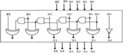
[image:3.612.196.413.239.336.2]The basic work is to use Binary to Excess-1 Converter (BEC) in the regular CSLA to get lower area and improved speed of operation. This logic is removed in RCA with Cin=1. This logic is implemented for different bits which are used in the modified design. The main advantage of this BEC logic comes from the fact that it uses low number of logic gates than the n-bit Full Adder (FA) structure. As stated above the main idea of this work is to use BEC instead of the RCA with Cin=1 in order to decrease the area and increase the speed. To remove the n-bit RCA, an n+1 bit BEC logic is required. The structure and the function table of a 8-bit BEC are shown in Figure 2.
Figure 2 .binary to excess-1 converter
III. ARCHITECTURE OF REGULAR 128-BIT SQRT CSLA
A 16 bit CSA can be designed in 2 different sizes namely uniform block size and variable block size. Similarly a 32, 64 and 128-bit can also be developed in two modes of different block sizes. Ripple carry adders are the simple and compact full adders, but its performance is limited by a carry that must spread from the least-significant bit to the MSB. The various 16, 32, 64 and 128-bit CSLA can also be designed by using ripple carry adders. The speed of a CSA can be enhanced upto 40% by performing the additions in parallel, and reducing the maximum carry delay. Fig 4 shows the Regular structure of 128-bit SQRT CSLA. It includes many ripple carry adders. The carry out of the Group 0 which acts as the selection input to mux which is in group 1, selects the result from the consequent RCA (Cin=0) or RCA (Cin=1). Similarly the remain groups will be selected depending on the Cout from the previous groups. In Regular CSLA, there is only one RCA to achieve the addition of the least significant bits [1:0]. The Cin from the previous parts selects one of the two RCAs. , If the carry-in is 0, the sum and carry-out of the upper RCA is selected, and if the carry-in is 1, the sum and carry out of the lower RCA is selected. For this Normal CSLA architecture, the execution code, for the Full Adders and Multiplexers of different sizes 6:3, 8:4, 10:5 were designed initially. The regular 64-bit, 128-bit CSLA were implemented by calling the ripple carry adders and multiplexers.
IV. ARCHITECTURE OF MODIFIED 128-BIT SQRT CSLA
Technology (IJRASET)
for Full Adder and Multiplexers of 6:3, 8:4, and 10:5 up to 24:11 were designed.
V. RESULTS
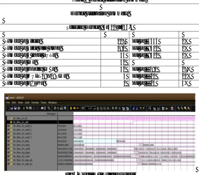
[image:4.612.111.501.250.594.2]The Proposed design in this work has been simulated using Verilog-HDL. The adders (of various sizes 16, 32, 64 and 128) are designed and simulated with Modelsim. After simulation the different size codes are synthesized using Xilinx ISE 9.1i. The simulated V files are imported into the synthesized tool and resultant values of delay and area are noted. The synthesized reports include area and delay values for different sized adders. The similar design flow is followed for both the regular and modified SQRT CSLA of different sizes. From the table it is clear that the delay decreases for 16-bit modified method when compared with regular method. The result table also shows the comparison for the various 32, 64, and 128 bits. The relative values of areas shows that the number of LUT will be more for modified the 16, 32 and 64. This value reduces gradually for 128 bits. For 256 bits the value almost equal to regular method which will decreases more for still higher order bits. Thus the modified method reduces the delay and also area to a great extent.
Table 1 Device utilization summary
Device utilization summary:
Selected Device : 3s500eft256-4
Number of Slices: 107 out of 4656 2%
Number of Slice Flip Flops: 182 out of 9312 1%
Number of 4 input LUTs: 53 out of 9312 0%
Number of IOs: 52
Number of bonded IOBs: 52 out of 190 27%
Number of MULT18X18SIOs: 4 out of 20 20%
Number of GCLKs: 1 out of 24 4%
Fig 3.moselsim simulation output
VI. CONCLUSION
Technology (IJRASET)
its performance matters the most while designing a digital FIR filter. Two different variations of carry save adders are designed using Verilog HDL. These adders are then integrated with the micro programmed FIR filters to further analyze the performance based on the area, power consumption and critical path delays. SQRT CSA delivers better performance than traditional adders for both the FIR filter architectures.
REFERENCES
[1] Bedrij, O. J., (1962), “Carry-select adder,” IRE Trans. Electron. Comput. Pp.340–344.
[2] Ramkumar,B. , Kittur, H.M. and Kannan ,P. M.,(2010 ),“ASIC implementation of modified faster carry save adder,” Eur. J. Sci. Res., vol. 42, no. 1,pp.53–58.
[3] Kim ,Y. and Kim ,L.-S.,(May2001), “64-bit carry-select adder with reduced area, “Electron Lett., vol. 37, no. 10, pp. 614–615.
[4] Ceiang, T. Y. and Hsiao. J., (Oct 1998), “Carry-select adder using single ripple carry adder,” Electron. Lett., vol. 34, no. 22, pp. 2101– 2103
[5] He, Y., Chang, C. H. and Gu, J., (2005), “An A rea efficient 64-bit square root carry-select adder for low power application,” in Proc. IEEE Int. Symp.Circuits Syst. vol. 4, pp. 4082– 4085.
[6] E. Abu-Shama and M. Bayoumi, “A New cell for low power adders,” in Proc.Int.Midwest Symp. Circuits and Systems, 1995, pp. 1014– 1017