International Journal of Emerging Technology and Advanced Engineering
Website: www.ijetae.com (ISSN 2250-2459,ISO 9001:2008 Certified Journal, Volume 5, Issue 5, May 2015)
Implementation of Static VAR Compensator (SVC) For
Power Factor Improvement
Amol P. Patil
1, Prof. P.V. Baviskar
21
ME Student, 2Associate Professor, Electronics Department, SSVPS, B.S.D.C.O.E. Dhule, Maharashtra, India
Abstract— Most of the loads (e.g. induction motors, arc
lamps) are inductive in nature and hence have low lagging power factor. The low power factor is highly undesirable as it causes an increase in current, resulting in additional losses of active power in all the elements of power sys-tem from power station generator down to the utilisation devices. A static VAR compensator consisting of capacitor bank in four binary sequential steps with a thyristor (SCR) controlled reactor of smallest step size is employed in the investigative work. This work deals with the performance evaluation through analytical studies and practical implementation on an existing system consisting of a distribution transformer of 1phase, 50Hz, 1KV/230V capacity. The PIC controller determines firing pulse of SCR to compensate excessive reactive power component for PF improvement. In order to ensure most favourable
conditions for a supply system from engineering and economical standpoint, it is im-portant to have power factor as close to unity as possible. In this paper, we shall discuss the methods of power factor improvement using PIC .
Keywords-- reactive power, static VAR compensator, capacitor bank, power factor
I. INTRODUCTION
We know that power loss is taking place in our low voltage distribution systems on account of poor power factor, due to limited reactive power compensation facilities and their improper control. In rural power distribution systems in wide spread remote areas, giving rise to more inductive loads resulting in very low power factors. It is necessary to closely match reactive power with the load so as to improve power factor and reduce the losses.The voltages at remote areas are low and farmers are using high power motors operating at low load with low efficiencies. In this paper, a more reliable, fast acting and low cost scheme is presented by arranging the thyristor switched capacitor units in four binary sequential steps. . Power companies convince their customers, which are with the large loads, to increase power factors of the supply above a specified amount( 0.90 or higher) or they should pay low power factor penalty. Some consumers with large loads use power factor correction schemes at their industry to avoid these penalty.The shunt capacitor improves the performance of feeder, shunt capacitor reduces voltage drop in the feeder & transformer.It provide better voltage at load end, improves power factor.It improves system security with enhanced utilization of transformer capacity, increases over all efficiency.
It saves energy due to reduced system losses, avoids low power factor penalty, and reduces maximum demand charges. Static Var Compensator is an automatic impedance matching device, it is designed to bring the system closer to unity power factor. SVCs are used in two main situations :a) Connected to the power system, to regulate the transmission voltage ("Transmission SVC"). b) Connected near large industrial loads, to improve power quality ("Industrial SVC").
1.1 Objectives Of Proposed Work
Fig.1: The proposed scheme for SVC.
The following expected outcomes are achieved by using microcontroller control signals to Static VAR Compensator (SVC) which fulfill the requirement of reactive power for a 1 PH, 50 Hz.
To maintaining the power factor at unity. To maintain minimum feeder current To improve the distribution feeder efficiency. To improve the voltage at load end.
To relief in maximum demand and effective utilization of transformer capacity.
To save the monthly bill on account of poor power factor, and results in maximum demand charges.
To conserve the energy.
1.2 Components of Proposed System:-
International Journal of Emerging Technology and Advanced Engineering
Website: www.ijetae.com (ISSN 2250-2459,ISO 9001:2008 Certified Journal, Volume 5, Issue 5, May 2015)
1. Thyristor/ Contactor Switched Capacitor (TSC/CSC) 2. ZCD V and ZCD I For Phase Shift Measurement. 3. Current Transformer (Ct) and Potential Transformer (Pt).
4. Signal Conditioning Unit. 5. PIC Controller Interface.
6. Isolation and Firing Circuit Of SCR.
II. STATIC VOLTAGE COMPENSATOR USING PIC
Fig.2: Arrangement for SVC using PIC.
Our work consists of following sections for measurement of current and voltage.
1. Current Transformer (CT) and potential Transformer (PT) .
2. Signal Conditioning Unit.
1. Current Transformer (CT) & Potential Transformer (PT):-
This is the input stage of the MDC system it actually senses the consumed power by load. Since the magnitude of voltage and current which can process these high level signals is difficult. So these signals are transformed into equivalent small level signals 0-230 V range is dropped to 0-6v by potential transformer and 0-15 a current is dropped to 0-50 mA current.
2.1 Signal Conditioning Circuit:-
This is the second block comprising precision rectifier. The line provided by electricity board carries ac signals of 50 Hz. After dropping these signals to low levels the
General Purpose IC OP07 is used as filters along with the diodes, resistors and capacitors. In ordinary bridge rectifier, there is a voltage drop in diodes. Diode will act as a rectifier within linear range only, before the knee point (.3v or .7v) output is zero. Thus the output of the rectifier is not exactly proportional to the input signal. A precision rectifier using op- amps is very accurate in this respect.
Fig.2.1: Signal Conditioning Block
The dc signal is then applied to the ADC. Out of 8 channels, chan0 is used for PT and chan1 is used for CT. As shown in circuit diagram the load lines are connected through CT & PT. The specification of CT and PT are as given.
a) Current Sensing Transformer ( CT)
Primary current up to 15 amp, Primary number of turns = 14
Primary wire gauge = 8 swg, Second number of turns = 250
Secondary wire gauge = 22 swg
Secondary voltage up to 5 volts with v burdon of 100 ohm.
b) Voltage Sensation Transformer (P.T) :-
Input Voltage = 230 v
Output voltage = 12v/500mA.
International Journal of Emerging Technology and Advanced Engineering
Website: www.ijetae.com (ISSN 2250-2459,ISO 9001:2008 Certified Journal, Volume 5, Issue 5, May 2015)
And after that potential divider arrangement is done using 1kΩ and 10kΩ trim pot is varied to achieved the linearity and scaling. This signal is applied to the precision rectifier. The working of the precision rectifier is as given.
In the circuit, diodes D1 and D2 are included within the feedback loop of the amplifier. If the diodes are non conducting the amplifier is effectively acting open loop and an input signal of magnitude VF /A0l is all that is required to the cause diode conduction ( Vf is the diode forward voltage drop ) Negative input signals cause diode D1 to conduct and the output signal which appears at the cathode of D1 is
(
)
The nonlinear diode resistance, since it is included within the feedback loop gain in the circuit and has negligible effect on the output signal. Positive input signals cut off diode D1 and cause D2 to conduct. This maintains the virtual earth at the inverting input terminal of the amplifier, and the output signal is zero since it is connected directly to this point via resistor R2.
Finally rectified DC voltage is passed through a active filter. For filter and precision rectifier general purpose op- amp 741 is used. CT signal is applied to channel 1 of ADC and PT signal is applied to channel 2 of ADC.
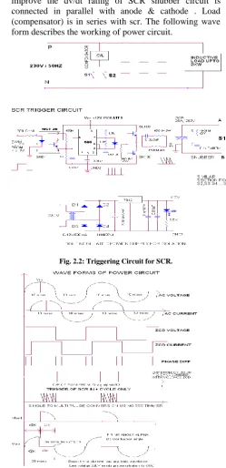
2.2 Triggering Circuit of SCR: -
While developing firing circuit it is assumed that,firing circuit may handle higher current rating (up to 25 A) whose gate drive requirement may be up to 0.1 A to 1 A. Just we have to replace SCR of higher rating only to handle a load of higher wattages.
Isolation is provided between power circuit and controller circuit using optocoupler MCT2E to limit the current of LED of optocoupler 330Ω Resistance is connected in series with anode of LED which is driven by a PWM pulse from the part of micro controller through a driver buffer 74245 o/p of the optocoupler is taken from emitter and is applied to reset pin of the 555 timer. 470K Ω will provide positive feedback. 1K Ω and 0.01Micro farad capacitor will provide stability.
Tc = 0.693 (RA + RB) C Td = 0.693(RB) C T = Tc + Td F = 1/T
Output of IC 555 timers is applied to push pull pair of transistor that is BC 547 /BC 557 or SL 100 / Sk 100 for current amplification which provides sufficient current to gate of SCR.
[image:3.595.303.553.198.714.2]To limit the gate current 390 Ω resistor and RC series combination is inserted between gate and push pull pair. Separate isolated +12V supply is provided to firing circuit. Power circuit consist of SCR 25ria12 having current rating up to 25 Amp and PIV rating 1200V to improve the dv/dt rating of SCR snubber circuit is connected in parallel with anode & cathode . Load (compensator) is in series with scr. The following wave form describes the working of power circuit.
[image:3.595.313.555.242.479.2]Fig. 2.2: Triggering Circuit for SCR.
International Journal of Emerging Technology and Advanced Engineering
Website: www.ijetae.com (ISSN 2250-2459,ISO 9001:2008 Certified Journal, Volume 5, Issue 5, May 2015)
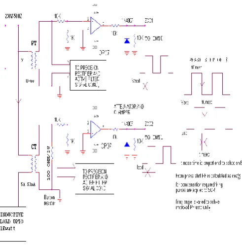
[image:4.595.51.297.149.399.2]2.3 Arrangment For Phase Shift Measurement
Fig.2.3: ZCD Block diagram for phase shift measurement.
Diode will act as clamper which convert bipolar signal to unipolar. Both the square wave signals for voltage & current will be given to INT0 & INT1 of PIC controller. When INT0 interrupt will occur then internal timer will start and it will stop at INT1interrupt. Time measurement by timer will give the respective phase shift in terms of Θ.
Display Unit:-
LCD module
LCD pin description:-
LCD displays are available typically as 16 x 12 or 20 x 2 along with LCD controller. 16 x 2 means 16 characters per line with 2 such lines. A standard LCD controller chip HD 44780U can receive data from a microcontroller and communicate with the LCD. In LCD module there are three control lines and 8 Data lines. The three control signals are enable (EN), register select (RS) and read/write RW.
VCC, VSS & VEE :- VCC and VSS provide + 5V and ground respectively. VEE is used for controlling LCD contrast.
III. PIC CONTROLLER INTERFACING DIAGRAM
PIC18F877A is PIC controller used for the system. The basic feature of PIC controller is it has inbuilt ADC (10-bit, 8channel) which can be used for current&
[image:4.595.315.552.222.442.2]PIC has three external interrupt which can be used for ZCD output for measurement of phase shift. It has Capture/Compare/PWM (CCP) modules which can be used to generate trigger pulses for SCR.The output of V and I measurement signal conditioning circuit i.e. V and I and also the output of ZCD circuit for V and I i.e. ZCD V and ZCD I are given to PIC18F458 microcontroller card.
Fig 3: PIC interfacing for static VAR compensator.
Fig.3 shows block diagram of PIC18F458 operation; in which inputs to controller are V analog, I analog, ZCDV, ZCD I while outputs from controller are PWM pulses to thyristors and signals consists of each parameters values to LCD display card for showing on display.
IV. RESULTS
Table no.1.
Observation For Inductive Load Without Compensation
S.N
Load VoltageCurrent Ph.Shift PF Act. P React.P
1. 200w 230 0.34A 0 DEG. 1 72W ---
2. MOTOR 1-100W 230 0.5A 45 0.70 76W 71W
3. MOTOR 2 230 0.63A 43 DEG. 0.71 106W 99W
4. 10W+10W+ MOTOR 1 230 1.26A 37 DEG. 0.86 240W 181W
5.
MOTOR 1+ MOTOR 2
International Journal of Emerging Technology and Advanced Engineering
Website: www.ijetae.com (ISSN 2250-2459,ISO 9001:2008 Certified Journal, Volume 5, Issue 5, May 2015)
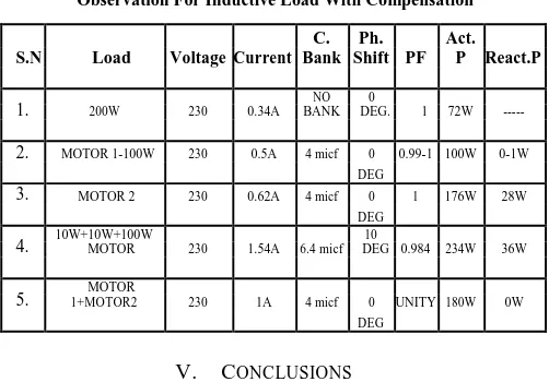
Table no.2.
Observation For Inductive Load With Compensation
C. Ph. Act.
S.N Load VoltageCurrent Bank Shift PF P React.P
1. 200W 230 0.34A BANK NO DEG. 0 1 72W ---
2. MOTOR 1-100W 230 0.5A 4 micf 0 0.99-1 100W 0-1W DEG
3. MOTOR 2 230 0.62A 4 micf 0 1 176W 28W
DEG
4. 10W+10W+100W MOTOR 230 1.54A 6.4 micf DEG 0.984 234W 10 36W
5. 1+MOTOR2 MOTOR 230 1A 4 micf 0 UNITY 180W 0W
DEG
V. CONCLUSIONS
From this paper our conclusion is that power factor of inductive load without compensation is not near to unity. With the help of static VAR compensator power factor improve near to unity for inductive load.
This method is used to
• To improve the voltage at load end.
• To relief in maximum demand and effective utilization of transformer capacity.
• To save the monthly bill on account of poor power factor, and
• To maintain the power factor at unity. • To maintain minimum feeder current • To improve the distribution feeder efficiency. • To conserve the energy.
REFERENCES
[1] “Hardware Circuit Implementation of Static VAR
Compensator(SVC)with Thyristor Binary Compensator” - Sameer U. Bagwan1, Anwar M. Mulla2, U. Gudaru3. International Electrical Engineering Journal (IEEJ) Vol. 5 (2014) No. 1, pp. 1240-1246.
[2] “PIC Microcontroller Based SVC for Reactive Power
Compensation and Power Factor Correction”- Abhinav Sharma1,
Vishal Nayyar2, S. Chatterji3, Ritula Thakur3, P.K.
Lehana*.International Journal of Advanced Research in Computer Science and Software Engineering, sept.2013.
[3] “Power Factor Improvement Technique Using Static
VARCompensator (SVC)”-Miss.S.D.Arote,Visiting Faculty
E&TC Dept, Govt. College of Engineering and Research Avasari Khurd, Tal:- Ambegaon, Dist:- Pune,2013.
[4] “The Experimental Studies of Transient Free Digital SVC
Controller with Thyristor Binary Compensator at 125 KVA Distribution Transformer”, Dadgonda R. Patil and Uppala Gudaru, IEEE Proceedings of the World Congress on Engineering 2012 Vol II, WCE 2012, July 4 - 6, 2012, London, U.K.
[5] “LC Compensators for Power Factor Correction of Nonlinear
Loads” Mohamed Mamdouh Abdel Aziz, Essam Din Abou
El-Zahab, Ahmed Mohamed Ibrahim. IEEE transactions on power delivery, vol. 19, no. 1, january 2004
[6] “A Static Synchronous Compensator for Displacement Power
Factor Correction under Distorted Mains Voltage Conditions” -R. Cimbals, O. Krievs, L. Ribickis Faculty of Power and Electrical Engineering, Riga Technical University,Kronvalda bulv. l- 2011
[7] “A Small Scale Static VAR Compensator for Laborat ory
Experiment” -Taufik* and Bryan Paet** Johor Baharu, Malaysia.
2nd IEEE International Conference on Power and Energy (PECon 08), December 1-3, 2008.
[8] “Hardware Circuit Implementation of Automatic Control of
Static VAR Compensator (SVC) using Micro
Controller”,VenuYarlagadda1,K.R.M.Rao2,B.V.Sankarram3
International Journal of Instrumentation, Control and Automation (IJICA) ISSN : 2231-1890 Volume-1, Issue-2,2011.
[9] PIC microcontroller & embedded system, Mazidi, 3rd Edition,
Pearson.
[10] “Power Electronics circuits devices and applications” M. H.
[image:5.595.38.289.149.324.2]