N A N O E X P R E S S
Open Access
Periodic nano/micro-hole array silicon solar cell
Guan-Yu Lai
1, Dinesh P Kumar
1and Zingway Pei
1,2,3*Abstract
In this study, we applied a metal catalyst etching method to fabricate a nano/microhole array on a Si substrate for application in solar cells. In addition, the surface of an undesigned area was etched because of the attachment of metal nanoparticles that is dissociated in a solution. The nano/microhole array exhibited low specular reflectance (<1%) without antireflection coating because of its rough surface. The solar spectrum related total reflection was approximately 9%. A fabricated solar cell with a 40-μm hole spacing exhibited an efficiency of 9.02%. Comparing to the solar cell made by polished Si, the external quantum efficiency for solar cell with 30 s etching time was increased by 16.7%.
Keywords:Metal catalyst; Nano/microhole Si array; Reflectance; Efficiency
Background
Previous studies have reported that nanostructure surfaces can efficiently couple incident light into semiconductors [1-3]. Efficient light harvesting is vital for solar cells [4,5]. In addition to light coupling, efficient carrier transport in a nanowire structure has been suggested to increase the short-circuit current [6-8]. Therefore, several studies on solar cells have employed nanostructures to enhance performance [9-15]. The difficulty in establishing contact in nanostructures limits progress. In one study, a conducting polymer was adopted because it easily filled the space between nanostructures, enabling high efficiency to be achieved [15]. Creating microholes might be an appropriate approach [16]; however, using microholes may cause the advantages of light harvesting to be lost. In this study, we propose a microhole array structure to facilitate fabrication by implementing metal catalyst etching. Inside the hole, we spontaneously produced a nanowire array to achieve low reflectance. The optical reflectance of nano/microhole arrays with various spacings was evaluated. A solar cell was manufactured using this structure to demonstrate the possibility of attaining high efficiency.
Methods
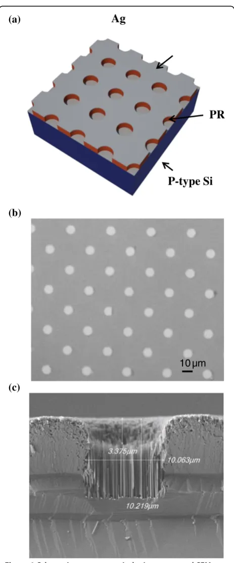
The microhole arrays were implemented using metal-catalyst etching on a (100) p-type Si wafer (1 to 10Ωcm). The wafer was cleaned using acetone in an ultrasonic bath for 10 min. After the substrate was rinsed with deionized (DI) water, it was immersed in a H2SO4and H2O2mixed solution for 10 min at 120°C. The substrate was further rinsed in DI water, blow-dried, and heated to 120°C in an oven. The microhole array pattern was implemented using photolithography. The diameter of holes on the photomask was 10μm. The spacing between the holes was varied from 10 to 40μm. To fabricate the microhole array, a Ag pattern was created by using the lift-off process for catalyst etching. The procedure is described as follows: a layer of photoresist (PR) was spin-coated onto the Si substrate. The Si substrate was then exposed to ultraviolet light through a photomask. After development, the PR on top of the Si substrate was patterned using a periodic hole array. A 50-nm-thick Ag was deposited onto the PR-coated Si substrate. A schematic diagram is shown in Figure 1a. After the PR was removed using acetone, a periodic Ag microdisk array with a diameter of 10 μm was obtained, as shown in Figure 1b. Metal-catalyst etching was conducted by immersing this sample into a H2O2/HF-mixed solution. Ag has a higher electron affinity than that of Si; therefore, the electrons in Si tend to accumulate on the surface of Ag. The H2O2 harvests these electrons and becomes H2O, as expressed in chemical reaction (1). The Si, lacking electrons, simultaneously reacts with H2O to form SiO2 and generate electrons, as expressed in chemical reaction (2). The HF then etches the SiO2 from the * Correspondence:[email protected]
1
Department of Electrical Engineering, National Chung Hsing University, 250 Ku-Kang Rd, Taichung 402, Taiwan
2
Graduate Institute of Optoelectronic Engineering, National Chung Hsing University, 250 Ku-Kang Rd, Taichung 402, Taiwan
Full list of author information is available at the end of the article
Ag, as expressed in chemical reaction (3). This process consumes no Ag and produces vertical Si patterns.
H2O2 þ 2Hþ þ 2e‐ → 2H2O ð1Þ
Si þ 2H2O → SiO2 þ 4Hþ þ 4e‐ ð2Þ
SiO2 þ 6HF → H2SiF6 þ 2H2O ð3Þ
A 10-μm-deep microhole after being etched for 15 min is illustrated in the cross-sectional scanning electron microscopy (SEM) image shown in Figure 1c. As shown in Figure 1c, the diameter of the hole is 10μm. Inside the hole, Si nanowires were clearly observed. After being etched, the Ag was removed using a HCl/ HNO3 (3:1 (v/v)) mixed solution. The structure was named‘nano/microhole array.’The n + emitter in a solar cell was fabricated by spraying H3PO4 onto a p-Si wafer and then annealing the sample in a furnace at 900°C for 30 min [17]. The doping concentration of phosphorus was calculated by converting the resistivity of Si into carrier concentration, in which the resistivity of Si was mea-sured by a spreading resistance profiler. By doping concentration profile, the phosphorus diffuse into Si around 0.2μm. The solar cells were then implemented by depositing top and bottom electrodes. The area of the solar cell was 1.0 cm2.
Results and discussion
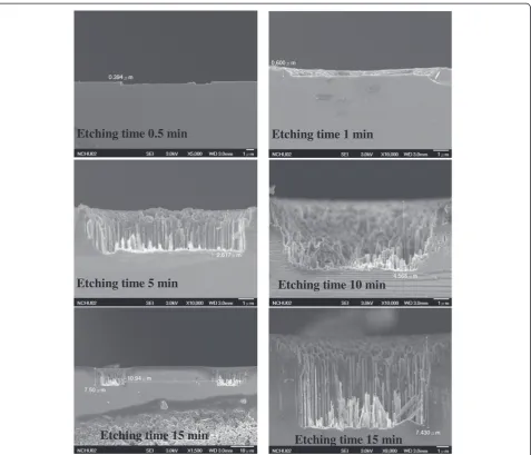
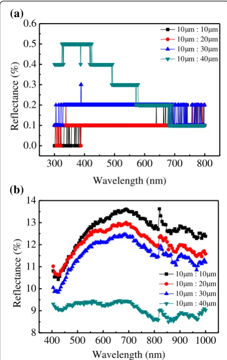
Cross-sectional SEM images of a nano/microhole array at various etching times are shown in Figure 2. The depths of the hole after 0.5, 1, 5, 10, and 15 min were 0.394, 0.6, 2.6, 4.57, and 7.5 μm, respectively. The etching rate was approximately 0.5 μm/min. The specular optical reflectance on nano/microhole arrays with various spacings was measured at a wavelength of 300 to 800 nm. The specular reflectance was well below 1% for all of the samples, as shown in Fig-ure 3a. The occurrence of the step-like reflectance is due to the resolution limit of the measurement, which is 0.1%. The microhole array sample with highest hole density (10-μm-spacing) exhibits lowest reflectance. In addition to the specular reflectance, the textured sur-face may cause the incident light scattered back to the incident plane, called diffuse reflectance. The total reflectance (Rtot) including specular and diffuse re-flectance was measured using an integrated sphere, as shown in Figure 3b. The highest Rtot was approxi-mately 14% for the 10-μm-spacing sample, whereas that of the 40-μm-spacing sample was 9%. The solar spectrum-related reflectance (Rsol) was 12.66%, 12.16%, 11.65%, and 9.21% for the samples with spacings of 10, 20, 30, and 40 μm, respectively. The Rsol was determined using the Equation (4):
(a)
P-type Si
PR
Ag
(b)
10 µm
[image:2.595.58.290.84.641.2](c)
Rsol¼ Z 800
300
Rtotð Þλ ⋅Ið Þλ ⋅dλ Z 800
300
Ið Þλ ⋅dλ
ð4Þ
whereI(λ) is the wavelength-dependent solar irradiance. Unexpectedly, the nano/microhole array with a large surface area (40-μm spacing) exhibited a low reflectance. This is not usual because a flat surface will cause specular reflectance only. The higher diffuse reflectance indicates the surface without hole array may not be flat. To prove this assumption, surface picture was taken by plan-view SEM. Figure 4a shows a SEM image of the Si surface. A porous surface was observed on the area that was not covered by Ag. The incoming light was scattered, causing the specular reflectance to be well below 1%. In addition, the porous-like surface scattered less incoming light than
did the periodic structure. Therefore, the sample with a spacing of 40 μm exhibited the least reflectance and is suitable for solar cell application. The mechanism that caused the development of the porous-like surface might be the dissociation of Ag in the H2O2/HF solution. During the etching process, Ag atoms can be converted into Ag+ ion by H2O2. The Ag+ion can be recovered back to Ag by taking electrons from silicon. This ionized and recovered process will lead Ag to diffuse up and renucleate on the undesigned silicon surface to form new etching sites [18]. A schematic diagram of Ag dissociation in the solution during etching is illustrated in Figure 4b. The dissociation of Ag produced a nanowire in the microholes as well as in the undesigned area. The photovoltaic characteristics were measured under a AM 1.5G condition by using a solar simulator (Model XES-40S1, San-EI Electric Co., Ltd., Osaka, Japan) equipped with an Agilent B2912A I-V
Etching time 0.5 min
Etching time 1 min
Etching time 5 min
Etching time 10 min
[image:3.595.61.539.87.496.2]Etching time 15 min
Etching time 15 min
meter (Agilent Technologies, Santa Clara, CA, USA). The dark current–voltage of the nano/microhole array solar cell with a hole spacing of 40μm at various etching times is shown in Figure 5a. No extensive dark current–voltage difference between the samples was observed. The photocurrent-voltage characteristics of the nano/micro-hole array solar cell are shown in Figure 5b. The device la-beled‘polish-Si’was a reference device for which no nano/ microhole array was composed. This device exhibited a 24.6-mA/cm2 short-circuit current density (Jsc), 537-mV open circuit voltage (Voc), and 0.7 fill factor (FF). The power conversion efficiency (η) was therefore 9.37%. By using metal-catalyst etching, the short-circuit current increased extensively. After only 0.5 min of etching, the
Jscincreased to 29.1 mA/cm2; this increase can be attrib-uted to the reflectance reduction after etching. However, the porous-like surface rendered achieving favorable
electrical contact difficult. The high contact resistance caused theFFto be low. Consequently, a low efficiency of 5.59% was obtained. After the etching time was increased to 5 min, theJsc did not increase. The contact resistance was reduced, possibly because the nano/microhole array provided a large surface area for contact. The Jsc de-creased to 25.5 mA/cm2as the etching time was increased to 10 min. This result is discussed in the subsequent para-graph. In a deep hole, the contact resistance substantially decreased. The series resistance reduced to 5.6Ω, which is near the value of polish-Si. In addition, theFFimproved to 0.65 and the efficiency increased to 9.02%. After the etching time was increased further to 15 min, the effi-ciency decreased to 6.9%. BothJscandFFdecreased. The decreased FF might be explained by the suddenly increased Rs. The Rs is expected to reduce as the hole-depth increase by the larger contact area. However, the formation of metal contact in this experiment is not by the metal paste, it is approximately 100 nm thick deposited by
(a)
300
400
500
600
700
800
0.0
0.1
0.2
0.3
0.4
0.5
0.6
10 m : 10 m 10 m : 20 m 10 m : 30 m 10 m : 40 m
Reflectance (%)
Wavelength (nm)
(b)
400
500
600
700
800
900 1000
8
9
10
11
12
13
14
Reflectance (%)
Wavelength (nm)
10 m : 10 m 10 m : 20 m 10 m : 30 m 10 m : 40 m
µ µ
µ µ
µ µ
µ µ
µ µ
µ µ
µ µ
[image:4.595.304.538.88.465.2]µ µ
Figure 3Specular and total reflectance of the nano/microhole array. (a)The specular reflectance of the nano/microhole array for different hole spacing.(b)The total reflectance of the nano/ microhole array for different hole spacing. The etching time is 15 min.
(a)
[image:4.595.57.288.89.455.2](b)
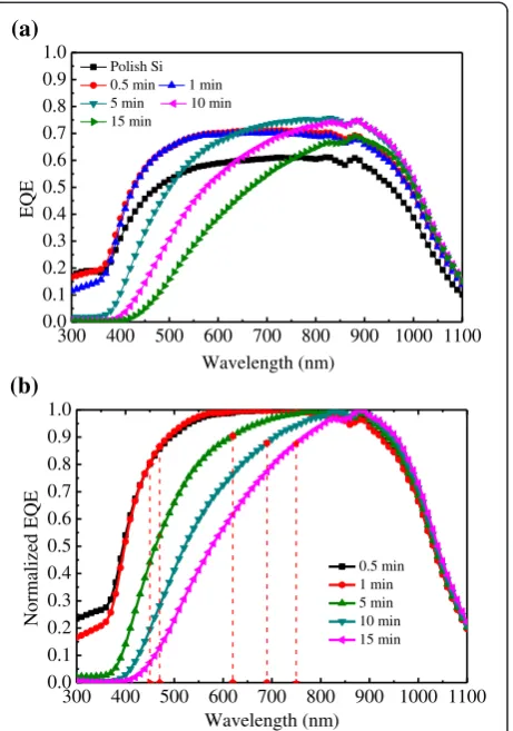
thermal evaporator. Therefore, in the deep hole, the metal line might be broken that causes the increasedRs. Table 1 lists details on the photovoltaic parameters. To explore the unusual trend in theJsc, external quantum efficiency (EQE) was measured. The EQE spectrum for the nano/microhole array solar cells at various etching times is shown in Figure 6a. The EQE for polish-Si was approximately
0.6 at a wide wavelength range and increased to 0.7 at an etching time of 0.5 min. However, the spectrum indicated that the EQE at a short wavelength decreased as the etching time was further increased, possibly because of carrier recombination at porous-like layers. The depth of the porous-like layer increased as the etching time was increased. The absorption of the incident light by the Si can be evaluated using Equation (5):
I dð ;λÞ ¼Ið0;λÞ⋅expð−α λð Þ⋅dÞ ð5Þ
[image:5.595.310.541.89.418.2]whereI(d,λ) refers to the intensity of light of wavelengthλ transmitted into Si at depthd;I(0,λ) refers to the intensity
Table 2 The depth of hole at specific etching time and the corresponding wavelength with the same absorption depth
Etching Time (min)
0.5 1 5 10 15
Depth (μm) 0.394 0.6 3.06 5.19 7.5
[image:5.595.56.294.89.447.2]Wavelength (nm) 450 470 620 690 750
Table 1 The photovoltaic parameters for the nano/micro hole array Si solar cell with different etching times
Etching time (min)
Jsc (mA/cm2) Voc (mV) FF η(%) Rs (Ω) Rsh (Ω)
Polish-Si 24.6 537 0.71 9.37 4.4 8,620
0.5 29.1 542 0.35 5.59 14.9 271
5 29.3 542 0.47 7.40 8.7 2,272
10 25.5 544 0.65 9.02 5.6 6,667
15 22.9 534 0.56 6.90 9.5 4,237
(a)
300 400 500 600 700 800 900 1000 1100
0.0 0.1 0.2 0.3 0.4 0.5 0.6 0.7 0.8 0.9 1.0
EQE
Wavelength (nm)
Polish Si 0.5 min 1 min 5 min 10 min 15 min
(b)
300 400 500 600 700 800 900 1000 1100
0.0 0.1 0.2 0.3 0.4 0.5 0.6 0.7 0.8 0.9 1.0
Normalized EQE
Wavelength (nm)
0.5 min 1 min 5 min 10 min 15 min
Figure 6External and normalized quantum efficiency of the solar cell. (a)The external quantum efficiency of the solar cell with different etching time.(b)The normalized external quantum efficiency of the solar cell with different etching time. The etching time ranged from 0.5 to 15 min.
(a)
-1.0 -0.5 0.0 0.5 1.0
10-5 10-4 10-3 10-2 10-1 100 101 102 103
Current density
(mA/cm
2)
Voltage (V)
0.5 min 5 min 10 min 15 min Polish Si
(b)
-0.4
-0.2
0.0
0.2
0.4
0.6
-5
0
5
10
15
20
25
30
35
Current density (mA/cm
2
)
Voltage (V)
0.5 min 5 min 10 min 15 min Polish Si
[image:5.595.57.290.642.732.2] [image:5.595.304.539.679.734.2]of the incident light at wavelengthλ; andα(λ) denotes the absorption coefficient of Si at wavelength λ in the unit 1/cm [19]. This equation indicated that a large amount of incident light is absorbed at depthd= 1/α. This depth was called the absorption depth. The depth of the hole at a specific etching time and the corresponding wavelength at the same absorption depth are listed in Table 2. Because the carriers generated by incident light at the depth of the porous-like layer have a high recombination rate, the EQE at a corresponding wavelength must be reduced. This assumption was explored using a normalized EQE spectrum. Figure 6b shows the normalized EQE for various etching times. The depth corresponding to the wavelength presented in Table 2 fits the reduction point of the EQE satisfactorily. The results indicated that the Jsc
can be further increased by appropriately passivating the porous-like layer by using methods such as oxidation. If the surface is well passivated, the optimum depth of hole is suggested to be approximately 20 to 25 μm by taking the light absorption edge of Si is approximately 900 to 950 nm.
Conclusions
In this study, we demonstrated the formation of a nano/ microhole array in Si by using a simple metal-catalyst etching method. The specular reflectance of this structure can be as low as 1%. The solar spectrum-related total reflection was approximately 9% for the 40-μm spacing sample. Efficiency of 9.02% was achieved by using this nano/microhole array without a surface passivation layer.
Competing interests
The authors declare that they have no competing interests.
Authors’contributions
ZP conceived of the study and participated in its design and coordination. GYL carried out the experiments on fabrication and SEM/optical measurements of the nano/microhole array and solar cell. DK contributed the mechanism discussion and drafted the partially manuscript. ZP revised the manuscript. All authors read and approved the final manuscript.
Acknowledgements
We thank the Ministry of Science and Technology of Taiwan for the financial support under grant NSC 102-2221-E-005-087.
Author details
1Department of Electrical Engineering, National Chung Hsing University, 250
Ku-Kang Rd, Taichung 402, Taiwan.2Graduate Institute of Optoelectronic Engineering, National Chung Hsing University, 250 Ku-Kang Rd, Taichung 402, Taiwan.3Nanoscience and Nanotechnology Research Center, National Chung Hsing University, 250 Ku-Kang Rd, Taichung 402, Taiwan.
Received: 30 June 2014 Accepted: 20 November 2014 Published: 3 December 2014
References
1. Raut HK, Ganesh VA, Nair AS, Ramakrishna S:Anti-reflective coatings: a critical, in-depth review.Energy Environ Sci2009,4:3779.
2. Pei TH, Thiyagu S, Pei Z:Ultra high-density silicon nanowires for extremely low reflection invisible regime.Appl Phys Lett2011,99:153108.
3. Thiyagu S, Devi BP, Pei Z, Chen YH, Liu JC:Ultra-low reflectance, high absorption microcrystalline silicon nano-stalagmite (μc-SiNS). Nanoscale Res Lett2012,7:171.
4. Hu L, Chen G:Analysis of optical absorption in silicon nanowire arrays for photovoltaic applications.Nano Lett2007,7(11):3249.
5. Muskens OL, Rivas JG, Algra RE, Bakkers M, Lagendijk A:Design of light scattering in nanowire materials for photovoltaic applications.Nano Lett
2008,8(9):2638.
6. Kayes BM, Atwater HA, Lewis NS:Comparison of the device physics principles of planar and radial p-n junction nanorod solar cells.Appl Phys Lett2005,97:114302.
7. Pei Z, Chang ST, Liu CW, Chen YC:Numerical simulation on the photovoltaic behavior of an amorphous-silicon nanowire-array solar cell. IEEE Electron Device Lett2009,30:1305–1307.
8. Kumar D, Srivastava SK, Singha PK, Husainb M, Kumar V:Fabrication of silicon nanowire arrays based solar cell with improved performance.Sol Energy Mater Sol Cells2011,95:215.
9. Peng K, Xu Y, Wu Y, Yan Y, Lee ST, Zhu J:Aligned single-crystalline Si nanowire arrays for photovoltaic applications.Small2005,1:1062. 10. Fang H, Li X, Song S, Xu Y, Zhu J:Fabrication of slantingly-aligned silicon
nanowire arrays for solar cell applications.Nanotechnology2008,
19:255703.
11. Stelzner T, Pietsch M, Andrä G, Falk F, Ose E, Christiansen SH:Silicon nanowire-based solar cells.Nanotechnology2008,19:295203.
12. Thiyagu S, Devi BP, Pei Z:Fabrication of large area high density, ultra-low reflection silicon nanowire arrays for efficient solar cell applications. Nano Res2011,4(11):1136.
13. Jung JY, Guo Z, Jee SW, Um HD, Park KT, Hyun MS, Yang JM, Lee JH:A waferscale Si wire solar cell using radial and bulk p–n junctions. Nanotechnology2010,21:445303.
14. Huang BR, Yang YK, Lin TC, Yang WL:A simple and low-cost technique for silicon nanowire arrays based solar cells.Sol Energy Mater Sol Cells2012,
98:357.
15. Thiyagu S, Hsueh CC, Liu CT, Syu HJ, Lin TC, Lin CF:Hybrid organic– inorganic heterojunction solar cells with 12% efficiency by utilizing flexible film-silicon with a hierarchical surface.Nanoscale2014,6:3361. 16. Chang YA, Li ZU, Kuo HC, Lu TC, Yang SF, Lai LW, Lai LH, Wang SC:
Efficiency improvement of single-junction InGaP solar cells fabricated by a novel micro-hole array surface texture process.Semicond Sci Technol
2009,24:085007.
17. Bouhafs D, Moussi A, Boumaour M, Abaïdia SEK, Mahiou L:N+silicon solar cells emitters realized using phosphoric acid as doping source in a spray process.Thin Solid Films2006,510:325.
18. Zhong X, Qu Y, Lin YC, Liao L, Duan XF:Unveiling the formation pathway of single crystalline porous silicon.ACS Appl Mater Interfaces2011,3:261. 19. Green MA, Keevers M:Optical properties of intrinsic silicon at 300 K.
Prog Photovolt1995,3:189.
doi:10.1186/1556-276X-9-654
Cite this article as:Laiet al.:Periodic nano/micro-hole array silicon solar cell.Nanoscale Research Letters20149:654.
Submit your manuscript to a
journal and benefi t from:
7Convenient online submission 7Rigorous peer review
7Immediate publication on acceptance 7Open access: articles freely available online 7High visibility within the fi eld
7Retaining the copyright to your article