N A N O E X P R E S S
Open Access
Conductive AFM for CNT characterization
Marius Toader
1*, Holger Fiedler
2, Sascha Hermann
2, Stefan E Schulz
2,3, Thomas Gessner
2,3and Michael Hietschold
1Abstract
We report on and emphasize the versatility of conductive atomic force microscopy in characterizing vertically aligned carbon nanotubes (CNTs) aimed to be used in via interconnect technology. The study is conducted on multi-walled CNT arrays vertically grown on a copper-based metal line. Voltage-dependent current mapping and current–voltage characteristics recorded down to single CNT allow for a comprehensive insight into the electric behaviour of the hybrid structure.
Keywords:Multi-walled carbon nanotubes, CNT, Conductive AFM, Atomic force microscopy, Interconnect system
Background
Starting with the pioneering work of Iijima [1], it is undeniable nowadays that the outstanding properties of carbon nanotubes (CNTs) recommend them for a wide range of applications as emphasized in a review article by Avouris et al. [2]. There is already more than one decade since the first successful report on CNT’s suitability for field-effect transistor applications [3] which started enor-mous aspiration toward CNT-based hybrid (nano)elec-tronics. However, the development of a novel hybrid technology is a slow process full of challenges. The most considerable drawback represents controlling and opti-mizing the quality of the CNT/metal contact. Especially, in vertical interconnect systems, this issue becomes of crucial importance. However, intense work was carried out in the last decade [4-10] to develop such CNT-based hybrid interconnect systems since outstanding properties like ballistic transport [11], high thermal conductivity [12,13] and capability to carry high current densities [7,14] earn them superiority over the traditional metals used cur-rently in the interconnect industry. For example, current densities up to 109A cm−2[14] and a thermal conductivity of 3,500 W m−1K−1[13] are 3 and 2 orders of magnitude superior to copper, respectively. Consequently, advanced hybrid interconnects where copper will be replaced by CNTs will represent the breakthrough in overcoming the actual limitations of the interconnect industry strongly con-strained by the shrinking issues. However, the quantum
resistance of CNTs requires for highly dense arrays integrated in parallel. Vertically grown CNTs using a bottom-up approach will fulfil this request and further-more increase the possibility of achieving narrower vias with higher aspect ratio. To successfully proceed with the development and improvement of such systems, a com-prehensive understanding is required and therefore a detailed characterization should be addressed. This is not an easy task since the downscaling tendency will require a characterization down to nanoscale where big challenges like confinement can occur. As a result, effects confined down to nanoscale can play a major and defining role in the overall performance of future devices. Therefore, not only the access of nanoscale is strongly required, but also the corresponding understanding is a key factor for reach-ing a success. Addressreach-ing these two aspects, the scannreach-ing probe microscopy techniques exhibit strong versatility. In particular, for interconnect systems, the electric characterization which gives an insight into the CNT/ bottom line contact quality is of great importance. Multi-walled CNT (MWCNT)-based via interconnect systems are mainly characterized in the literature using classical electrical measurements where the entire via is contacted using a top metal electrode. It is obvious where the prob-lem lies in this configuration. The outcome of the study tells nothing about fluctuations inside the via itself. The interpretation of such results is rather blind relative to a possible inhomogeneous internal performance. Via a (nano)characterization of such systems by conductive atomic force microscopy (c-AFM), this issue is not over-looked. Moreover, c-AFM gives the opportunity to address single CNTs earning undeniable superiority over the * Correspondence:[email protected]
1
Solid Surfaces Analysis Group, Institute of Physics, Chemnitz University of Technology, Chemnitz 09107, Germany
Full list of author information is available at the end of the article
classical electrical measurements. While general informa-tion can be collected over an extended CNT array using the so-called current mapping, individual CNTs can be addressed in detail using current–voltage (I-V) studies. The facility is crucial as the downscaling tendency boosts the importance of the CNT/metal contacts in the ultimate nanoscaled devices with a strong impact over the final performance. Therefore, c-AFM was applied in this work to address the electric characterization of vertically aligned MWCNT arrays grown on a copper-based metal line.
Methods
Vertically aligned MWCNT arrays were grown by chem-ical vapour deposition on a copper-based conductive metal line as comprehensively described in [8,15]. The copper-based metal line is a layer stack where Ta was used as the top layer. Moreover, TaN was used as the barrier layer to inhibit copper diffusion into the Ni cata-lyst layer. It was shown that the lack of such a diffusion barrier would strongly affect the quality of the CNT ver-tical growth [8]. All data shown within this work were recorded under ambient conditions using a 5500 AFM from Agilent Technologies (Santa Clara, CA, USA). N-type (phosphorus-doped) silicon-etched AFM probes from MikroMasch (Wetzlar, Germany) with a nominal uncoated tip radius of 10 nm were used for
tapping-mode imaging. In contact-tapping-mode imaging, conductive AFM probes are required in order to simultaneously obtain the corresponding current map. The Ti-Pt coat-ing material consists of a 10-nm Pt layer on top of a 20-nm Ti sublayer and is formed on both tip and reflec-tive side of the cantilever, leading to a nominal tip radius of around 40 nm. In the conductive AFM setup, a spe-cial nose cone with a built-in preamplifier is used for current detection when a bias voltage is applied between the sample and the cantilever. The two-terminal setup uses the conductive AFM probe as the first electrode (which contacts the top end of the MWCNTs) and a metallic wire as the second electrode (which contacts the bottom metal line via a large area of MWCNTs co-vered with silver paste). Every I-Vset shown within this work is, on average, over ten spectra recorded in the same contact point. One hundred points within the indi-cated voltage range and 2-s acquisition time were used for individual spectrum.
Results and discussion
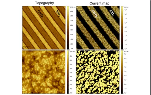
Classical topography vs. current map AFM images are displayed in Figure 1. They can be simultaneously recorded in c-AFM configuration operating in contact mode. Trench-like CNT arrays are separated via SiO2as
[image:2.595.57.540.415.718.2]marked in Figure 1. When a sample bias of 500 mV is
applied, a current flow is generated between the bottom metal line and the metallic tip via the vertically aligned MWCNTs. While a strong signal from the CNT arrays can be identified in the current map, there is no current detected at the SiO2 side. At a first view, the system
seems to exhibit a perfect homogeneous conductivity within the MWCNT arrays. However, the observation is misleading since the measured current exceeds the ma-ximum 10 nA detectable with our system.
Therefore, the current map is recorded within the sat-uration regime which can be avoided using much lower sample biases as it will be shown later on. However, at this point, it is sufficient to emphasize a successful electric connectivity of the CNTs to the bottom metal line. High resolution down to single MWCNT is acces-sible via AFM. The corresponding electric response can be addressed as well, which earns AFM superiority over the classical electric measurements where the entire MWCNT array is contacted using top electrodes. Deter-mining the CNT density and taking into consideration the AFM tip radius, it was obtained that the AFM tip gets in contact with (1.1 ± 0.1) CNTs [15]. What can be seen in the highly resolved AFM image is only the top end of the MWCNTs. The CNTs are well embedded in a SiO2matrix to ensure stabilization during chemical–
mechanical planarization. It can be observed from the corresponding current map that the current flows ex-clusively at the CNT site and drops immediately to zero at the SiO2 site, indicating the lack of lateral leakage
currents.
The lateral resolution is well known to be tip-convoluted, and therefore, a reliable CNT diameter estimation is not possible from these measurements. Especially, in c-AFM
where the AFM tip is rastering in contact mode at the sam-ple surface, the tip convolution is greater since the metal coating leads to an enlarged tip radius. There exist some reports where this issue is carefully addressed and solutions are proposed.
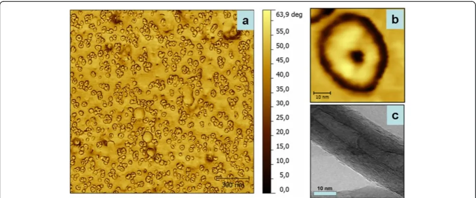
For example, in lying CNTs, the tip diameter estimation is done according to the height appearance which however was shown to become problematic for larger diameters due to the tip-induced deformation which results into a non-circular cross section of the CNT [16]. To reduce the tip convolution and to further increase the lateral resolution in c-AFM down to 1 nm, Hong et al. [17] have manufactured an atomic-size metallic filament on a commercial AFM probe. In our case, using the conventional tapping mode, the tip convolution can be considerably reduced. Here, un-coated pure silicon tips allow for recording high-resolution AFM images with much better improved lateral resolution. Furthermore, phase imaging provides a better contrast where the edges of individual CNTs can be distinguished more easily. The top end of individual CNTs appears as a disc-like shape with a shallow depression in the middle (see Figure 2a). According to the grain size statistics, a mean value of 20 nm was obtained with a filling percentage of 43%. A highly resolved AFM phase image of an indivi-dual CNT is displayed in Figure 2b. A corresponding transmission electron microscopy (TEM) image of a single MWCNT grown under the same conditions is shown in Figure 2c. There can be observed a very good agreement between the AFM and TEM images concern-ing the tube diameter.
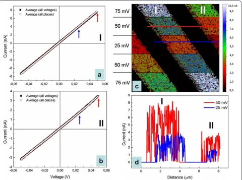
[image:3.595.57.539.502.703.2]If the current map is recorded using a much lower sam-ple bias of only 25 mV, variations in the electric response between distinct CNT arrays can be observed despite the
good inside homogeneity (see Figure 3a). A detailed in-sight into the electric behaviour can be addressed byI-V spectroscopy. Here, two types of experiments were per-formed. On one hand, different initial sample biases were used to check if there is any influence on theI-V spectros-copy of presumably different initial loading forces induced
[image:4.595.59.539.89.225.2]by slight variations in the electric field between the metal-lic tip and the MWCNTs expected to be metalmetal-lic. On the other hand, I-Vspectroscopy was performed on distinct locations to get an insight into the MWCNT array homo-geneity. The average spectra for the selected MWCNT arrays I and II are displayed in Figure 4a,b, respectively.
Figure 3Current map and the correspondingI-Vcharacteristics.Current map (a); the correspondingI-Vcharacteristics for the indicated MWCNT arrays in (a) recorded under different initial sample voltages (b) on different locations (c).
Figure 4AverageI-Vcharacteristics of MWCNT arrays, voltage-dependent current map and corresponding profile lines.The averageI-V
[image:4.595.59.540.348.705.2]The outcome proves that none of both experiments influences somehow the electric response and sustains a very good reproducibility of the I-Vspectroscopy. The estimated average error bar approaches 2% and 4% relative to the average resistance determined for the selected I and II MWCNT arrays, respectively. Similar conductivity obtained on distinct locations supports the current mapping in what concerns the good homogen-eity inside individual MWCNT arrays. The obtained linear I-Vspectra indicate that the metallic character of the MWCNTs is in good agreement with the results obtained from Raman spectroscopy and TEM studies [8]. It is more important to highlight that the formation of the MWCNT/metal contact preserves the metallic be-haviour which however is not always necessarily the case. Furthermore, voltage-dependent current mapping allows probing the electric response upon a couple of sample biases at one glance (see Figure 4c). This type of study is mostly recommended and helpful for very small objects like, for example, lying CNTs, where the tip posi-tioning and consequently a reproducible tip-CNT con-tact geometry becomes problematic. However, in this case, it can be furthermore used to check the correlation with the I-Vspectroscopy. In Figure 4d, two profile lines are depicted for two different sample biases, namely 50 mV (red line) and 25 mV (blue line) (refer to Figure 4c as well). The pointing-up arrows (refer to Figure 4a,b) obeying the same colour code indicate the current values obtained via I-V spectroscopy for the previously mentioned sample biases. A very good agreement between the I-V spectros-copy and the voltage-dependent current mapping can be clearly observed. The outcome looks very promising in investigating long and narrow nano-objects. As, for example, a lying single-walled CNT (with a length in the micron range but a diameter of only 1 nm) can pre-sumably be very accurately sectioned via the voltage-dependent current mapping rather than performing un-certain I-Vspectroscopy with random tip-CNT contact geometry. The few obtainedI-Vpoints will be sufficient
to get a trend and therefore an insight into the electric behaviour (linear or non-linear).
A similar study can be successfully extended at larger scale as can be observed from Figure 5. The same good analogy can be made between the voltage-dependent cur-rent mapping and theI-Vspectroscopy. In both cases, var-iations in the electric response could be emphasized from array to array.
[image:5.595.61.541.91.219.2]The estimated resistances of the investigated MWCNT arrays are included in Table 1. As shown previously, an error bar up to 4% might occur. Despite the relative high magnitude, the resistance values will however be consi-derably reduced (some orders of magnitude) for the overall highly dense vias where vertically aligned CNTs will be integrated in parallel. For example, using a rough estimation, within a 2-μm-diameter via, there can be ideally integrated (100% filling percentage) up to 10,000 MWCNTs with a diameter of 20 nm. However, if a simi-lar filling percentage can be assumed as the one previ-ously estimated, a correction factor of slightly larger than 2 should be included. Still, a reduced resistance of up to 3 orders of magnitude is expected to characterize the entire via. In our setup, it must be mentioned that the estimated resistances contain, besides the internal CNT resistance, inputs from metal contacts, namely me-tallic tip/CNT and CNT/bottom metal line. Whilst the first-mentioned top contact resistance is constant (due to the same loading force) and the CNT quality is pre-sumably the same (Raman spectroscopy confirmed this issue on a similar sample [15]), the observed variation in the electric response from network to network is due to the bottom contact resistance. At the moment, it can be concluded that the electric behaviour of the bottom
Figure 5Topography (a) vs. voltage-dependent current map (b); correspondingI-Vcharacteristics of indicated MWCNT arrays (c).
Table 1 The estimated resistance values of the indicated MWCNT arrays
MWCNT array I II III IV V
[image:5.595.304.540.706.734.2]contact layer is inhomogeneous. The reason behind is mostly due to the formation of tantalum oxide and tantalum carbides as could be emphasized by energy-filtered TEM [15] which however requires for ultimate sample damage. In this regard, it was shown that c-AFM gives the extra possibility to electrically investigate bur-ied interfaces to a very low scale being superior in this regard to the standard I-V measurements which exhibit a strong average character.
Conclusions
The final message of this work emphasizes the versatility of c-AFM to investigate vertically aligned MWCNT arrays aimed for via interconnect systems in a highly reproducible manner. Such studies can bring in parallel to the 3D topography substantial advantages over the
standard I-V measurements. Complementary
informa-tion confined down to extremely low scales is accessible. This might be of great relevance for future studies on extremely narrow CNTs via interconnects where the im-portance of individual CNTs grows considerably, espe-cially possible variations in the electric behaviour from individual CNTs can occur. Complementary to the clas-sical electric measurements where top contacts are required and therefore a general electric behaviour for the whole via is obtained, c-AFM can address individual CNTs and get a better detailed insight into the via. The outcome can prove itself of crucial importance in com-prehensively understanding and consequently optimizing the development of via interconnect systems.
Competing interests
The authors declare that they have no competing interests.
Authors’contributions
MT performed all the AFM measurements and wrote the manuscript. HF and SH developed the technology behind the sample preparation and consequently prepared the samples. Corrections to the manuscript were also provided. SS, TG and MH put the basis of the entire project, guided the internal collaboration, and read and improved the manuscript. All authors read and approved the final manuscript.
Acknowledgements
This work was supported by the Deutsche Forschungsgemeinschaft (DFG) via the Research Unit 1713‘Sensoric Micro and Nano Systems’and GRK 1215
‘Materials and Concepts for Advanced Interconnects’.
Author details
1
Solid Surfaces Analysis Group, Institute of Physics, Chemnitz University of Technology, Chemnitz 09107, Germany.2Center for Microtechnologies,
Chemnitz University of Technology, Chemnitz 09126, Germany.3Fraunhofer Institute for Electronic Nano Systems, Chemnitz 09126, Germany.
Received: 16 July 2012 Accepted: 7 December 2012 Published: 11 January 2013
References
1. Iijima S:Helical microtubules of graphitic carbon.Nature1991,354:56–58. 2. Avouris P, Chen Z, Perebeinos V:Carbon-based electronics.Nature Nanotech
2007,2:605–615.
3. Tans SJ, Verschueren ARM, Dekker C:Room-temperature transistor based on a single carbon nanotube.Nature1998,393:49–52.
4. Kreupl F, Graham AP, Duesberg GS, Steinhögl W, Liebau M, Unger E, Hönlein H:Carbon nanotubes in interconnect applications.Microelectronic Eng2002,64:399–408.
5. Li J, Ye Q, Cassell A, Tee Ng H, Stevens R, Han J, Meyyappan V:Bottom-up approach for carbon nanotube interconnects.Appl Phys Lett2003,
82:2491–2493.
6. Yokoyama D, Iwasaki T, Ishimaru K, Sato S, Hyakushima T, Nihei M, Awano Y, Kawarada H:Electrical properties of carbon nanotubes grown at a low temperature for use as interconnects.Jpn J Appl Phys2008,47:1985–1990. 7. Sato M, Hyakushima T, Kawabata A, Tatsuhiro N, Sato S, Nihei M, Awano Y:
High-current reliability of carbon nanotube via interconnects.Jpn J Appl Phys2012,49:105102-1–105102-4.
8. Fiedler H, Hermann S, Schulz SE, Gessner T:Influence of copper on the catalytic carbon nanotube growth process. In2011 IEEE International Interconnect Technology Conference and 2011 Materials for Advanced Metallization (IITC/MAM): May 8–12 2011; Dresden. New York: IEEE; 2011:1–3. 9. Fayolle M, Pontcharra J, Dijon J, Fournier A, Okuno H, Quesnel E, Muffato V, Jayet C, Lugand JF, Gautier P, Vandroux L, Huet S, Grampeix H, Yckache K, Mariolle D, Billon T:Innovative scheme for selective carbon nanotubes integration in via structures.Microelectronic Engineering2011,88:833–836. 10. Chiodarelli N, Masahito S, Kashiwagi Y, Li Y, Arstila K, Richard O, Cott DJ,
Heyns M, De Gendt S, Groeseneken G, Vereecken PM:Measuring the electrical resistivity and contact resistance of vertical carbon nanotube bundles for application as interconnects.Nanotechnology2011,22:085302. 11. Poncharal P, Berger C, Yi Y, Wang ZL, de Heer WA:Room temperature
ballistic conduction in carbon nanotubes.J Phys Chem B2002,
106:12104–12118.
12. Kim P, Shi L, Majumdar A, McEuen PL:Thermal transport measurements of individual multiwalled nanotubes.Phys Rev Lett2011,
87:215502-1–215502–4.
13. Pop E, Mann D, Wang Q, Goodson K, Dai H:Thermal conductance of an individual single-wall carbon nanotube above room temperature. Nano Lett2006,6:96–100.
14. Wei BQ, Vajtai R, Ajayan PM:Reliability and current carrying capacity of carbon nanotubes.Appl Phys Lett2001,79:1172–1174.
15. Fiedler H, Toader M, Hermann S, Rodriguez R, Sheremet E, Rennau M, Schulze S, Waechtler T, Hietschold M, Zahn D, Schulz S, Gessner T:
Distinguishing between individual contributions to the via resistance in carbon nanotubes based interconnects.ECS J Solid State SciTechnol2012,
1(6):M47–M51.
16. Alizadegan R, Liao AD, Xiong F, Pop E, Hsia KJ:Effects of tip–nanotube interactions on atomic force microscopy imaging of carbon nanotubes. Nano Res2012,5:235–247.
17. Hong SS, Cha JJ, Cui Y:One nanometer resolution electrical probe via atomic metal filament formation.Nano Lett2011,11:231–235.
doi:10.1186/1556-276X-8-24
Cite this article as:Toaderet al.:Conductive AFM for CNT characterization.Nanoscale Research Letters20138:24.
Submit your manuscript to a
journal and benefi t from:
7 Convenient online submission 7 Rigorous peer review
7 Immediate publication on acceptance 7 Open access: articles freely available online 7 High visibility within the fi eld
7 Retaining the copyright to your article