Article
1
Application-specific oxide-based and metal-dielectric
2
thin film materials prepared by RF magnetron
3
sputtering
4
Mohammad Nur-E-Alam *, Wade Lonsdale, Mikhail Vasiliev, and Kamal Alameh
5
Electron Science Research Institute, School of Science, Edith Cowan University, 270 Joondalup Drive,
6
Joondalup 6027, WA, Australia.; E-mails: [email protected] (M.N.A), [email protected]
7
(M.V), [email protected] (W.L) and [email protected] (K.A)
8
* Correspondence: [email protected]
9
Abstract: We report on the development of several different thin-film functional material systems
10
prepared by RF magnetron sputtering at Edith Cowan University nanofabrication labs. We conduct
11
research on the design, prototyping, and practical fabrication of high-performance magneto-optic
12
(MO) materials, oxide based sensor components, and heat regulation coatings for advanced
13
construction and solar windows.
14
Keywords: thin films; coatings; magneto-optics; sensors; glass; heat regulation.
15
16
1. Introduction
17
Among all the physical vapor deposition techniques, magnetron sputter deposition is one of the
18
most common technologies used to grow thin film materials and coatings for various existing and
19
modern nano-technological applications. Sputter deposition of thin films has a long track record of
20
development history in vacuum technology since 1800s [1-10]. Many dedicated research groups and
21
scholars were involved in the development of the modern phase of magnetron sputtering technology,
22
although the journey of the magnetron sputtering process is still considered far from its ultimate
23
development [6, 8]. However, nowadays the magnetron sputtering is considered one of the most
24
effective processes for the deposition of a wide range of high-quality thin-film materials either in
25
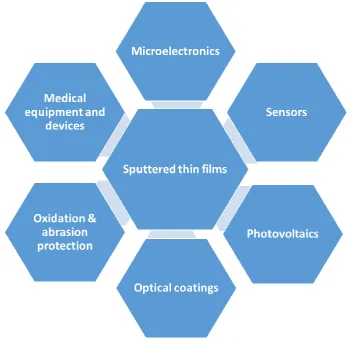
single or multilayer form, including metals, dielectrics, metal oxides of complex stoichiometry, and
26
nanoparticles. A vast number of sputtered material types were shown to be suitable for various
27
existing and emerging nanotechnology-related applications, and attractive for many rapidly growing
28
diverse market sectors. Sputtering processes allow to deposit thin-film materials either on bare
29
substrates or on top of any structured systems, e.g. photonic or magneto-photonic crystals, usually
30
without having any unpredictable thickness uniformity or stoichiometry issues with the grown films.
31
Thin-film materials, especially radio frequency (RF) magnetron sputtered thin films were originally
32
considered useful mainly in electronics and semiconductor devices, however, sputtered thin films
33
have also been found to be applicable within a wide range of fields such as optoelectronics, energy,
34
mechanical/chemical, optical coatings, life sciences, and others [9–29]. In this nano-technological era,
35
the sputter-deposition of thin films becomes a rather ubiquitous and actively growing field of human
36
endeavour, integrating the fundamental and important scientific areas of research, process
37
development, deposition-system design, and new product manufacturing. This trend is expected to
38
continue into the periods extending far into the foreseeable future. The reasons behind the rapid
39
growth of the sputtering industry over other thin film manufacture techniques include (i) possibility
40
of using large-area sputtering targets that provide uniform film thickness over large-area substrates;
41
(ii) flexibility of growing thin or extremely ultra-thin film materials of various composition types
42
(even complex stoichiometry types, e.g. oxide-mix-based iron garnet precursors) on different
43
substrate types; (iii) ease of controlling the film thickness by calibrating the deposition run times and
44
other parameters; (iv) better layer-to-substrate adhesion quality, compared to techniques such as
45
thermal evaporation. Also, the successful establishment of deposition technologies for thin polymer
46
films and metal/plasma polymer nano-particles fabrication using polymer or metal-polymer
47
composite targets in RF magnetron sputtering systems by optimizing the process gas chemistries (e.g.
48
argon, nitrogen), shows the diversity of thin-film types grown by RF magnetron sputtering [30-33].
49
Figure 1 presents a wide range of possible application areas of sputtered thin films for the continued
50
exploration by future generations.
51
52
53
54
Figure 1. Spectrum of modern nano-technological application areas reliant on sputtered thin-film materials.
55
56
Based on the current and possible future emerging applications, the global market of sputtered
57
thin films can be subdivided into many segments. According to the report [34] made by PR Newswire
58
in 2017, the sputtered thin films market volume including sputtering-related equipment, raw
59
materials, and services, amounts to approximately one-quarter of the total estimated (over US $70
60
billion) value of global markets of thin-film technologies in 2016, and is expected to grow at a
61
significant rate. However, according to the MarketWatch report published in 2018, the thin film
62
materials market is expected to witness a substantial growth from 2018 to 2024, due to the demand
63
for miniaturization of thin-film related technologies, devices, and products. In addition, the
64
increasing number of applications and end-use industry practices are also expected to propel the
65
growth of the thin-films product markets in the near future [35].
66
67
In this paper, we discuss the experimental results selected from a decade-long lab-based work,
68
during which the RF sputtering synthesis of different thin-film material types and multilayer
69
structures have been explored extensively. We also present and discuss the specific material
70
development results and functional material properties of interest for several specific applications.
71
The organization of the article is as follows. Section 2 introduces the background study of
Bi-72
substituted iron garnet thin-film materials and multilayers together with some very recently obtained
optical properties for highly bismuth-substituted iron garnets of composition type Bi2Dy1Fe4Ga1O12
74
(BiDyIG). These garnet composition types (with bismuth substitution levels above about 1.8) can only
75
be prepared using physical vapour deposition techniques (e.g. sputtering), and have not been
76
reported synthesized by crystal growth techniques such as liquid-phase epitaxy. Section 3 describes
77
the design, fabrication and characterization of ruthenium oxide (RuO2) thin films grown on rigid and
78
flexible substrates, for sensor applications. Section 4 describes the fabrication techniques and process
79
parameters used for growing metal-dielectric nano-composite (MDC) layers and MDC layers
80
contained within multilayer structures for use in next-generation environment-friendly highly
81
durable optical coatings for solar and thermal radiation control. The optical properties of these MDC
82
thin-films and multilayer building blocks containing nanocomposite-type materials are presented in
83
this section.
84
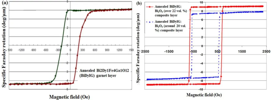
85
2. Garnets, garnet-oxide composites, and multilayer structures manufactured by sputtering
86
Natural garnets are popular as gemstones, but when they are engineered either by modifying their
87
stoichiometry or by adjusting the fabrication process, they can possess extra-ordinary multifunctional
88
properties that make them attractive for various applications e.g. integrated photonic circuits and
89
devices. Through nano-engineering, garnet thin films can be controlled, at the atomic level, to attain
90
naturally-unachievable photonic and magnetic properties that open the way towards the
91
development of magnetophotonic and magneto-plasmonic crystals (MPCs) for a wide range of
92
applications, including telecommunication, biomedicine, digital forensics, sensing and data
93
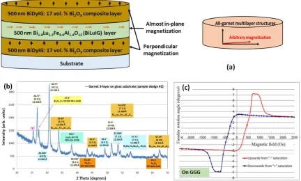
processing. Thin-film garnets have a long history that started since these were developed in 1960 for
94
the first time for use in bubble memory device applications [36-55]. The properties of thin garnet films
95
are always dependent on their fabrication methods, process parameters and especially on the
96
stoichiometry of the material. By varying the materials compositional constituents together with their
97
optimized fabrication process parameters in RF magnetron sputtering systems, the magnetic and
98
magneto-optic properties of garnet thin films can be tailored for specific applications. Multiple
99
research groups worldwide [56-65] have conducted a significant number of research works using
100
only RF magnetron sputtering to synthesize, develop and improve many garnet thin-film material
101
systems. Since the last decade, a number of highly bismuth (Bi) substituted iron garnet thin-film
102
material systems including garnet-oxide and garnet-garnet nano-composite derivatives, have been
103
synthesized, their sputtering process parameters optimized, and many studies of the optical,
104
magnetic and magneto-optical properties were reported by our group at ECU [66-73]. We have
105
reported obtaining nano-crystalline garnet thin-film materials with high Faraday rotation across the
106
visible spectral range, a record-high magneto-optic quality, very low coercive force with
107
perpendicular magnetization and almost in-plane magnetization types. Also, a rather unconventional
108
magnetic switching properties have recently been demonstrated in all-garnet multilayer thin film
109
structures. In this section, we present the recently obtained results on the optical constants of RF
110
sputtered highly Bi-substituted iron-garnet precursors of nominal composition type Bi2Dy1Fe4Ga1O12
111
(BiDyIG) and garnet-oxide composites (GOC), together with a glimpse of the previously
best-112
achieved MO properties in thin garnet films of similar compositions. The unconventional hysteresis
113
loop shapes observed in GOC-based all-garnet multilayer structures are also presented.
114
Figure 2(a) shows the measured transmission spectra of as-deposited Bi2Dy1Fe4Ga1O12 (BiDyIG)
115
garnet and BiDyIG: Bi2O3 (17 & 23.3 vol. %) composite thin film layers prepared on glass substrates
116
by using RF magnetron co-sputtering process. These particular garnet types possessed MO garnet
117
compositions (and optical properties) of special importance in common application areas, e.g.
118
Faraday rotators, ferromagnetic resonance-based microwave devices, MPCs, and MO imagers. In the
119
co-sputtering process, two separate oxide-mix-based ceramic targets (Bi2Dy1Fe4Ga1O12, and Bi2O3)
120
were used and the materials volumetric fraction ratios were controlled and calculated from their
121
partial deposition rates. The details of several GOC layer deposition technologies and sputtering
122
process parameters are described in Refs. [66, 68-70]. From the thickness-dependent
wave interference fringes intensities (measured over a wide range of wavelengths in all samples, Fig
124
2a), using a new combinatorial approach, the optical constants of amorphous garnet-precursor layers
125
are calculated and refined, together with the film thickness confirmation [73]. This combinatorial
126
approach employs a custom-built spectrum-fitting software in conjunction with Swanepoel envelop
127
method (SWEM). The following operational steps are conducted for the evaluation of optical
128
constants: (i) calculation of the refractive index data and film thickness using the SWEM method[74];
129
(ii) use of the calculated index data (from SWEM), in conjunction with least-square fitting to derive
130
the real part of index from Cauchy’s formula (n (λ) = a + b/λ2); (iii) use of the refractive index data
131
(derived from Cauchy’s formula) in magnetic photonic crystal (MPC) analysis software [75] to model
132
and fit the measured transmission spectra, and (iv) from this fitting process, reconfirm the film
133
thicknesses and derive the absorption coefficient spectra of the films. The wavelength-dependent
134
index (n) data ( calculated based on Cauchy’s dispersion formula) for the amorphous garnet and
135
garnet-oxide precursor thin layers deposited on glass (Corning Eagle XG, 0.5 mm thick) substrates,
136
yields the following spectral dependency for BiDyIG sample, n = 2.1906 + 0.0459/λ2, and for BiDyIG:
137
Bi2O3 (17 vol. %) composite sample, n = 2.2105 + 0.0576/λ2; for BiDyIG: Bi2O3 (23.3 vol. %) composite
138
sample, index dispersion function n = 2.1961 + 0.0683/λ2 was obtained.
139
140
Figure 2. (a) Measured transmission spectra of as-deposited Bi2Dy1Fe4Ga1O12 (BiDyIG) and BiDyIG: Bi2O3 (17 &
141
23.3 vol. %) composite thin films, (b) derived refractive index dispersion spectra for Bi2Dy1Fe4Ga1O12 (BiDyIG)
142
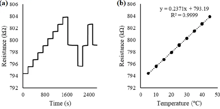
and BiDyIG: Bi2O3 (17 & 23.3 vol. %) composite thin films where the solid curves were determined according to
143
Cauchy dispersion relationship.
The calculated refractive indices at different wavelengths derived from Cauchy’s relation as well
145
as the calculated refractive index data points using the SEWM method were plotted and compared
146
(as shown in Fig. 2b). It can be noted that the refractive index (n) is in the range of 2.2-2.6 in the visible
147
region and decreases with increasing wavelength. In the long-wavelength region (above 1600 nm),
148
the refractive index seems to be asymptotically approaching a constant value. The volumetric fraction
149
of excess Bi2O3 introduced into the BiDyIG system helps increase the refractive index of the composite
150
films, however, this also shifts the absorption edge towards the shorter wavelength region (as seen
151
in Fig.2a). Note that there are always significant differences that exist between the optical constants
152
of the crystallized garnets and oxide-mix-based amorphous precursor layers. Therefore, it is also
153
important to check the conformity of layer(s) to their designed spectral transmission specifications
154
before annealing, especially when developing functional multilayer structures, such as MPC.
155
In our previous work, we have observed the effects of excess Bi2O3 addition to core materials
156
within each garnet-related oxide mix (a generic composition type can be defined using a formula
157
description such as (Bi,Y,Dy,Lu,…)3(Fe,Al,Ga,…)5O12) on their annealing crystallization behaviour,
158
and the final optical/MO properties. It was reported that an optimized amount of extra Bi2O3 content
159
addition, can significantly improve the specific Faraday rotation, optical transparency and optical
160
absorption coefficient across the visible spectral range, thus leading to achieving record-high MO
161
quality factors in suitably annealed garnet-oxide composite thin films [66, 68]. Figure 3 shows the
162
typical magnetic hysteresis loop properties of annealed garnet and GOC films measured through
163
specific Faraday rotation at 532 nm using a Thorlabs PAX polarimeter system in conjunction with a
164
custom-made calibrated electromagnet. Noteably, the annealed BiDyIG sample showed a nearly
165
square-shaped hysteresis loops of Faraday rotation (Fig. 3a), whilst the annealed GOC films often
166
showed practically perfectly “square” shapes of hysteresis loop (Fig. 3b) with perpendicular
167
magnetic anisotropy, high (close to 100 %) remnant magnetization, and very sensitive magnetic
168
switching behaviour.
169
170
Figure 3. Hysteresis loops of specific Faraday rotation at 532 nm measured in sputtered garnet films. (a)
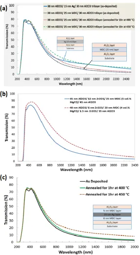
171
Annealed (nanocrystalline) Bi2Dy1Fe4Ga1O12 (BiDyIG) sample, and (b) annealed BiDyIG: Bi2O3 composite-type
172
oxide-diluted thin films [66].
173
The strong uniaxial magnetic anisotropy in BiDyIG: Bi2O3 nano-composite films together with some
174
degree of control over the coercive force and switching field properties (as shown in Fig. 3b) and
175
excellent optical and magnetic properties, make them very attractive and promising for a large range
176
of optoelectronic, photonics-related, sensing, and MO imaging applications.
177
We observed somewhat unconventional and remarkable magnetic switching properties for the
178
first time in RF magnetron sputtered all-garnet multilayer thin-film structures, in which
magneto-179
soft layers were sandwiched in-between two magneto-hard garnet material layers of identical
180
composition type [76]. Both garnet material types possessed very large specific Faraday rotation
across the visible spectral range (≈ 6 °/µm at 532 nm and ~ 1.6 °/µm at 635 nm [66, 68]) and high
182
magneto-optic (MO) quality. The magnetic switching behavior of trilayers (illustrated in Fig. 4a),
183
were characterized by way of measuring their Faraday rotation hysteresis loops. The samples were
184
prepared on glass (Corning Eagle XG) and also GGG (111) substrates; the sputtering deposition was
185
followed by post-deposition annealing crystallization (heat treatment process, 1 h at 570 °C)
186
conducted in air atmosphere. The amount of extra bismuth oxide content co-sputtered from a
187
separate target (17 vol. %) was selected to facilitate a notable increase in the specific Faraday rotation
188
whilst at the same time avoiding a significant reduction in the upper limits of the annealing
189
temperature range. X-ray diffraction (XRD) measurements (performed in the range of 2θ angles
190
between 20° and 70°, as shown in Fig. 4b) revealed the body-centered cubic lattice structure of
191
different constituent garnet materials present inside annealed trilayers. Their microstructure type has
192
been identified as being nanocrystalline on both substrate types. A notable and unexpected feature
193
of hysteresis loop behavior (Fig. 4c) was the presence of an “intermediate saturation” state exhibiting
194
the maximum Faraday rotation, which then was followed by conventional magnetization saturation
195
state with reduced Faraday rotation, at increasing external magnetic fields above about 1 kOe. The
196
final saturated Faraday rotation was observed at near 1.6 kOe, at below 50% of the maximum Faraday
197
rotation angle seen at smaller fields. To the best of our knowledge, no prior (or later) reports of similar
198
magnetic switching behaviours observed in any thin-film materials, relative to Ref. 76, can be found
199
in the published literature. These exchange-coupled all-garnet multilayer structures demonstrated an
200
attractive combination of optical and magnetic properties, and are of interest for emerging
201
applications in optical sensors and isolators, ultrafast nanophotonics, magneto-plasmonics and
202
possibly spintronics.
203
204
Figure 4. The schematic diagram of all-garnet multilayer structures together with the predicted layer-specific
205
magnetization vector directions (a); XRD analysis results obtained from a multilayer garnet structure prepared
206
on a glass substrate (b); the unconventional magnetic hysteresis loop of Faraday rotation (°) measured using
207
green laser light source.
208
The objective of making this all-garnet trilayer structure was to investigate the potential of
209
obtaining and controlling these special magnetic switching properties observed in the described
210
trilayer types that are not attainable normally in any single-layer magnetic thin films. We note that
211
the unconventional magnetic behavior has only been observed in trilayers employing co-sputtered
nanocomposite-type outer magneto-hard layers. Further studies are on-going, aimed at achieving
213
better control over the magnetic properties (e.g. coercive force, switching field(s), and saturation
214
magnetization) in garnet multilayer structures having different combinations of high-performance
215
garnet materials of various optimized thicknesses as well as stoichiometry types. Other active areas
216
of ongoing research within our group include the investigations of the effects of the post-deposition
217
oxygen plasma treatment of amorphous-phase garnet-precursors on the final magnetic and MO
218
properties observed in crystallized films. Initial findings indicate that there exist optimized oxygen
219
plasma post-treatment regimes, which lead to observing strong improvements in the MO quality of
220
annealed thin garnet layers.
221
3. Ruthenium-oxide thin-films grown on flexible and rigid substrates for cost-effective sensor
222
electrodes
223
Sputter-deposition process parameters such as total or partial gas pressure(s), process gas
224
chemistry, substrate type, substrate-stage heating temperature, substrate-stage rotation rate,
225
substrate-to-target distance, target rotation rate, and RF powder densities, are well-known to affect
226
the growth and properties of thin-film materials. There are many reports published in the literature
227
describing the necessity of sputter-deposition process parameter optimization for many
application-228
specific oxide-based and other thin-film materials [78-88]. For example, sputter-deposition process
229
parameters were studied and optimized to deposit ruthenium oxide (RuO2) thin films with strong
230
adhesion properties for manufacturing durable sensing electrodes [84, 88]. For the manufacture of
231
sensors, it is important to control the material properties in order to obtain the desired functionality
232
[89]. In this section, we present optimized R.F. sputter-deposition process parameters for the
233
manufacture of highly-durable RuO2 thin-film electrodes on flexible and rigid substrates, along with
234
the pH and temperature sensing performance of these electrodes.
235
Ruthenium oxide thin films feature very attractive properties for use in various sensing devices,
236
such as pH sensing, cryogenic temperature sensing, and even bio-sensing applications [90-92]. In
237
order to manufacture durable and therefore cost-effective electrodes, it is important to have strong
238
adhesion of RuO2 to its substrate material. This requires optimization of multiple sputter-deposition
239
process parameters, to overcome sputter-chamber pressure-dependent adhesion properties of RuO2
240
layers fabricated on different substrates [90].
241
242
3.1. Experimental
243
244
RuO2 thin-film electrodes (potentiometric, interdigitated and resistive) were deposited directly
245
onto two different substrate materials (alumina and polyimide), as shown in Figure 5. In summary,
246
100 nm thick layers of RuO2 were deposited using RF magnetron sputtering from a metal-oxide (RuO2)
247
target (99.95% purity) with 110 W sputter power, at room temperature, with 4 mTorr chamber
248
pressure and 5:5 sccm Ar:O2 gas flow rate. Electrode patterns were achieved using a standard
249
photolithographic process.
252
253
Figure5. 100nm thick potentiometric, interdigitated and resistive RuO2 electrodes sputter deposited on alumina
254
(a) and polyimide (b) substrates.
255
256
Potentiometric measurements were made using an Atlas Scientific ORP EZO circuit connected
257
to PC via an Electrically Isolated USB EZO Carrier Board, with a commercially available glass
258
Ag|AgCl|3M KCl reference electrode (Sigma). Resistive electrodes were characterized with an
259
Agilent 34410A high performance digital multimeter, using a 2-wire set-up to measure resistance.
260
Measurements were made using commercially available buffer solutions (Rowe Scientific), for pH.
261
Whilst, temperature was controlled using a thermoelectric device and insulation.
262
263
3.2. Results and comparison
264
265
RuO2 films sputter deposited directly onto flexible polyimide substrates can be a cost-effective
266
choice for use as a potentiometric electrode. It has been found experimentally that the
polyimide-267
based electrodes prepared using a 4 mTorr chamber pressure and 1:1 Ar: O2 gas ratio, showed
268
excellent performance when used as potentiometric pH electrode (vs. Ag|AgCl|KCl reference
269
electrode), exhibiting a reversible (±3.9 mV), linear (R2=0.9994) and Nernstian (57.5 mV/pH) pH
270
response, as shown in Fig. 6. The obtained result is comparable to previously reported RuO2 pH
271
electrodes prepared on alumina substrates, which also exhibited a reversible (±1.8 mV), linear
272
(R2=0.9999) and Nernstian (59.1 mV/pH) pH response [90]. The polyimide resistive and interdigitated
273
electrodes failed when used as conductivity and temperature sensors, due to gradual delamination.
274
However, the alumina-based resistive temperature sensor exhibited reversible (± 0.01 °C) linear
275
(R2=0.9999) response, which is comparable to some commercially available sensors as shown in Fig.
276
7.
279
280
Figure 6. Electric potential recorded vs. a Ag|AgCl|KCl reference electrode for the potentiometric RuO2
281
electrode on polyimide substrate, in pH 2, 4 7, 10 and 12 buffers (a), and the reversible linear Nernstian pH
282
response of the electrode (b).
283
284
285
286
Figure 7. Electric resistance variations recorded for a RuO2 electrode on alumina substrate, at 5 to 45 ºC (a), and
287
the reversible linear temperature response of the electrode (b).
288
289
To summarize, durable metallic RuO2 thin films could only be deposited with a chamber
290
pressure ≥ 4 mTorr with argon: oxygen content in the chamber. RuO2 films deposited at pressures
291
lower than 4 mTorr produced powdery films that rapidly delaminate from all substrates. The
292
improved durability of these RuO2 electrodes allows for the development of reliable sensors,
293
potentially for miniaturised applications or where conventional glass probes are not suitable, such as
294
biomedical applications.
295
296
Other RF sputtered metal oxide materials investigated by our group included rare-earth oxide
297
compositions such as Er2O3, Dy2O3, Gd2O3, and other, e.g. Zr2O3,TiO2, SnO2, and Al2O3. Intended
298
applications included the scratch-proof and hydrophobic film layers, sensing applications, diffusion
299
protection layers, and generic multilayer constituents. Two principal categories of deposition
300
processes were explored with oxide materials: sputtering in pure-argon plasma and the processes
301
run using argon-oxygen plasma mixes. Substantial differences in the resulting oxide material
302
properties were observed, dependent on the deposition process type used. The main reason for the
observed property differences was the oxygen loss occurring during sputtering deposition, which
304
has often been possible to recover using high-temperature oven annealing processes.
305
4. Metal-dielectric nanocomposite-based multilayer building blocks for transparent solar and
306
thermal regulation coatings
307
The development of modern energy-efficient glass and window products requires specialized
308
thin-film coatings containing silver (Ag) layer(s) to filter or reflect the infrared and far-infrared
309
(thermal) radiation components of the solar spectrum, thus reducing the energy consumption in
310
buildings. Also, surface plasmon resonance-based optical sensors require noble metal-dielectric
311
interfaces, and have numerous commercial applications in gas, biochemical and chemical sensing
312
due to their high sensitivity to the refractive index changes in a dielectric medium placed on top of
313
ultra-thin metallic (Ag) films [93-96]. The deposition of the ultra-thin Ag layers with low surface
314
roughness and high uniformity is the key to achieving the required application-specific optical
315
properties. However, the deposition of ultra-thin (less than 20 nm) Ag layers often results in forming
316
morphologically uneven nano-islands, even when using the fine-tuned deposition processes, such as
317
RF magnetron sputtering [97, 98]. The formation of these Ag nano-islands significantly affects the
318
optical performance of multilayer metal-dielectric thin-film structures. Typically, reduced reflectivity
319
across the near-infrared range results from the imperfect metal layer morphologies. Also, dielectric
320
material layer deposited on top of these island-shaped ultra-thin Ag layers tend to “sink” into the
321
spaces between these silver nano-islands, leading to strong optical property deviations from the
322
designed response. Another issue associated with Ag is that it oxidizes very quickly, therefore the
323
Ag layer has to be protected from oxidation even during the deposition of the next material layer in
324
the thin-film multilayer sequence. Researchers have proposed and trialled the preparation of
325
nanocomposites to overcome these issues related to the difficulties of forming ultra-thin Ag layers.
326
Most of the relevant success stories were about depositing metal-dielectric nano-particle based
327
composites [99-103].
328
We have prepared sputtered metal-dielectric nanocomposites (MDC) by developing a
co-329
sputtering process for Ag-MgF2 system, with various volumetric contents of the dielectric phase
330
added to the metal. We have also developed MDC-containing multilayer structures, and their
331
characterisation results suggest that MDC layers can replace the pure-metal layers in multilayer
332
optical coatings, thus offering a new possibility to design and fabricate highly durable and
333
environmentally-stable coatings on glass suitable for solar and thermal regulation technologies [104].
334
In this section, we present the growth process details for thin-film single-layer MDC and newly
335
developed MDC-containing multilayer coatings. Their measured optical characteristics are also
336
reported. The transmission spectrum features of these newly-developed MDC-based multilayer
337
building blocks appear to be promising for manufacturing cost-effective solar and thermal heat
338
regulation coatings for the construction industry, in the near future.
339
340
4.1 Deposition of MDC layers and multilayer structures
341
342
Several batches of MDC (Ag+MgF2) films were deposited onto glass substrates by using the
co-343
sputtering process in an RF magnetron sputtering system. The volumetric fraction of dielectric (MgF2)
344
phase was controlled by adjusting the RF power densities applied to the MgF2 sputtering target
345
during the co-sputtering process, after carefully calibrating the partial deposition rates for both MgF2
346
and Ag. The thicknesses of ultrathin composite films trialled were in the range between 12 - 25 nm.
347
After the successful growth of MDC layers, we prepared several multilayer structures introducing
348
the optimized MDC layers along with surrounding oxide layers. Table 1 summarizes the deposition
349
process parameters used to fabricate these metal-dielectric nanocomposite layers and MDC
350
containing multilayer building blocks. The transmission and reflection spectra of MDC layers were
351
measured just after the deposition using an Agilent Cary 5000 UV-VIS-NIR spectrophotometer. The
352
reflection spectrum measurements were carried out using a custom-built reflection-mode optical
measurement module mounted inside the spectrophotometer, which contained four mirrors adjusted
354
at 45-degree tilts to form a periscope-type device as shown in Fig. 8.
355
356
Table 1. Sputtering process parameters used to deposit MDC single layer and MDC containing multilayer
357
building blocks.
358
359
Process parameters Layer structure (single layer MDC)
Layer structure (multilayers containing MDC layer) Sputtering targets Ag, MgF2 Al2O3, Zr2O3, Ag, MgF2 RF Power Ag (55-65 W), MgF2 (83-95
W)
Al2O3 (190 - 195 W), Ag (55 - 65 W), MgF2 (83 - 95 W) Base pressure (Torr) 5 × 10⁻⁶ 5 × 10⁻⁶
Process gas Ar Ar
Process pressure 2-3 mTorr 1-3 mTorr
Substrate temperature (°C) Room temperature Room temperature Post deposition heat treatment No Up to 500°C for 1-10 hours
360
361
362
363
Figure 8. Schematic diagram of the optical system used in Cary 5000 spectrophotometer to measure the
364
reflection spectrum of the thin film coatings on glass substrates.
365
366
Since our primary motivation for MDC materials development was to broaden the range of
367
possible high-performance designs of heat-mirror-type coatings, and because the reflectivity of these
368
coating types across the near-infrared range is their main performance indicator, developing both the
369
transmission and reflection spectral measurements was necessary.
370
371
4.2 Optical characteristics of MDC thin films and MDC-containing multilayer structures
372
373
Figure 9 shows an example of the measured transmission and reflection spectrum of Ag+MgF2
374
(5 vol. %) composite (~20 nm) thin-film. The transmission peak in this Ag+MgF2 composite layer
375
exhibited short-wavelength transmission and reflection features similar to the Ag layer of the same
376
thickness. The optical absorption was calculated by subtracting the transmittance and reflectance of
377
the composite layers using the formula A=1-T-R (%), where A is the absorbed power fraction, T is the
378
power transmission coefficient, and R is the power reflectivity. It was found that the Ag+5 vol. %
379
MgF2 sample had a comparatively lower absorption (less than 9 % by power) in the UV-Visible
380
spectral range, which is close to that of the pure Ag layer. This indicates that the addition of 5 vol. %
381
MgF2 into the Ag layer during the co-sputtering process can potentially improve the coating adhesion
382
and stability aspects without compromising the plasmonics metal properties.
385
386
Figure 9. Measured transmission and reflection spectra of ~ 20 nm thick Ag+ 5 vol. % MgF2 composite layer,
387
deposited onto glass substrate.
388
389
Several trilayer structures containing at least one MDC layer were deposited on clear glass
390
substrates using one continuous sputtering run, and their optical performance was characterized.
391
Figure 10 (a) shows the transmission spectrum of as-deposited multilayer coatings, where the layer
392
structure consists of at least one MDC (Ag + 4-5 vol. % MgF2) in comparison to that of a typical
tri-393
layer pure metal (Ag) based DMD-type coating. It can be noted that the use of a 25 nm MDC layer
394
instead of a pure 15 nm Ag layer resulted in better thermal radiation filtering performance without
395
compromising the visible spectral transmission, whilst avoiding any potential layer
morphology-396
related issues that usually affect ultrathin (thinner than about 17nm) layers. Experimental
397
investigations revealed that the co-sputtered MDC (even comparatively thicker) layers with high
398
metal volume content can be embedded into any type of multilayer structures for possibly improving
399
the spectrally-selective transparency control, and structural properties of the coating whilst allowing
400
significant design flexibility. Particularly important is the possibility of depositing MDC-type layers
401
onto practically any underlying film layers, almost regardless of surface energy-related layer
402
interface compatibilty considerations. The MDC based structures also demonstrated much lower
403
thermal emissivity whilst maintaining the same superior visible transmission compared to the
silver-404
based coatings, as shown in Fig. 10(a).
408
409
Figure 10. Measured transmission spectra of multilayer thin film structures containing a single (or double)
410
metallic or MDC layer. (a) Transmission of a tri-layer MDC structure compared to that of a typical Ag layer
411
within a DMD structure; thermal performance stability test results are also shown for the tri-layer MDC structure;
412
(b) transmission spectra of multilayer structures containing MDC layer of different volumetric fractions of added
413
dielectric, and (c) thermal performance stability test results for a complex DMD-type multilayer structure
414
containing both the MDC outer-bracket sublayers and an ultra-thin pure-Ag core layer.
415
416
In order to investigate the design variations, material intercompatibility, durability and thermal
417
stability properties of the MDC-based coatings, several different types of test multilayers (up to
five-418
layer structures) were developed, as shown in Fig. 10 (b, c). Figure 10 (b) shows the optical
419
performance of an elementary (five layer-based) thin-film coating building blocks composed of a
420
center MDC layer, surrounded by thin oxide-based “bracket layers” deposited by pure-argon
421
sputtering process from a ceramic oxide target of Zr2O3. The addition of these ultrathin rare-earth
oxide layers has led to broadenening the structure design possibilities in terms of improving the peak
423
transmission and spectral selectivity. The optical performance variations observed in this particular
424
five layer-based coatings confirmed the possibility of engineering a broader range of optical coatings
425
for future solar and thermal regulation application in comparison with a simple
dielectric-metal-426
dielectric (DMD) trilayers or multilayers of similar spectral response. Figure 10(c) presents a more
427
complex generalized MDC-type multilayer building block, which was subjected to extensive thermal
428
stability (dry heat exposure) tests. The performance of the developed structure (before and after heat
429
exposure in an air-filled lab oven) shows that the optical properties are comparable to some of the
430
conventional multilayer structures containing pure Ag layers [105, 106]. It can be seen clearly that the
431
transmission spectra were found to be only slightly changed at temperatures near 400 °C, which is a
432
very encouraging result, and confirms that the very thin MDC barrier layers can play a vital role in
433
protecting the ultra-thin core Ag layers within the multilayer structures. This confirms that the MDC
434
layers can be used to enable arbitrarily complex high-stability low-E, heat-mirror, or filter-type
435
optical coating designs of high spectral selectivity, on a range of optical substrates. Additionally, it is
436
possible to engineer a broader range of reflected or transmitted colour properties, compared to pure
437
metal-based designs, which are much more limited in terms of the optical materials selection.
438
439
5. Conclusions
440
We demonstrate a range of material system design possibilities for multiple practical
441
applications provided by fine-tuning the RF magnetron sputtering technologies. We established
442
numerous sputtering-based thin-film material synthesis processes at ECU, aiming at incorporating
443
these optical materials into functional devices for sensing, optical spectra shaping, polarisation
444
control, magnetic switching, and magnetic field visualization, among others. Three functionally
445
different categories of thin-film material systems have been discussed, such as MO garnets, metal
446
oxides, and metal-dielectric nanocomposites, and results have been presented describing their
447
growth processes and relevant parameters, physical properties, and behavior. All of the characteristic
448
results obtained from these material system types are of interest for use in practical field-specific
449
applications in optics, magneto-optics, sensing, and renewable energy.
450
451
Author Contributions: All authors have made nearly equal contributions to the study and manuscript. M. N. A.
452
planned and designed the manuscript. M. N. A., W. L., and M. V. discussed the contents and wrote the
453
manuscript, K. A. revised the manuscript, and edited it further, contributing to the final group discussion
454
outcome regarding the manuscript.
455
Funding: This research work is supported by Electron Science Research Institute, Edith Cowan University, WA,
456
Australia. No external funding was received.
457
Acknowledgments: The authors would like to acknowledge Dr. Yamna El-Mouedden for making some
458
characterization experiments with MDC-based thin films and for generating the results presented in Figure 9
459
also Fig. 8.
460
Conflicts of Interest: The authors declare no conflict of interest.
461
References
462
1. Grove, W. R. On the electro-chemical polarity of gases. Philos. Trans. R. Soc., 1852, Vol. 142, 87-101.
463
2. Wright, A. W. On the production of transparent metallic films by the electrical discharge in exhausted
464
tubes. Am. J. Sci. Arts.,1877, Vol. 13, 49-55.
465
3. Greene J. E. Review Article: Tracing the recorded history of thin-film sputter deposition: From the
466
1800s to 2017. J. Vacuum Science & Technology A,2017, 35, 05C204-1-60.
467
4. Lakhtakia, A.; Messier, R. Nanoengineered Morphology and Optics, SPIE-The International Society for
468
Optical Engineering, Bellingham, Washington, USA, 2005, Chapter-2, 27-48.
5. Alfonso, E.; Olaya, J.; Cubillos, G. Thin film growth through sputtering technique and its applications.
470
https://www.intechopen.com/books/crystallization-science-and-technology/thin-film-growth-471
through-sputtering-technique-and-its-applications.
472
6. Mattox, D. M. A short history: Magnetron sputtering deposition.
473
https://www.svc.org/DigitalLibrary/documents/2015_Summer_DMM.pdf.
474
7. Depla, D.; Mahieu, S.; Greene, J. E. Sputter deposition processes.
475
https://core.ac.uk/download/pdf/55744819.pdf.
476
8. Anders, A.; Mattox, D. M. Magnetron Sputtering: An Unfinished Journey, Tutorial presentation, 58th
477
Annual Technical Conference of the Society of Vacuum Coaters (April, 2015): available on,
478
www.svc.org.
479
9. Mattox. D. M. The Foundations of Vacuum Coating Technology. William Andrew, The Boulevard,
480
Langford Lane, Kidlington, Oxford, OX5 1GB, United Kingdom, and 50 Hampshire Street, 5th Floor,
481
Cambridge, MA 02139, United States, 2018, Elsevier Inc.
482
10. Sarkar, J. Sputtering Materials for VLSI and Thin Film Devices. William Andrew, 2010, ISBN,
978-0-483
8155-1593-7
484
11. Lu, D. X.; Wong, E. M. W.; Pun, E. Y. B.; Chung, P. S.; Jia, G. C. PZT thin films by radio frequency
485
magnetron sputtering. In: Lampropoulos G.A., Lessard R.A. (eds) Applications of Photonic
486
Technology 2. Springer, Boston, MA, https://doi.org/10.1007/978-1-4757-9250-8_9.
487
12. Lin, K. T.; Wu, J. M. RF-magnetron sputtering of Titanium dioxide for microelectronics
488
applications. J. J. Appl. Phys., 2004, Vol. 43 (1-1), 232-236.
489
13. Sakthivel, P.; Murugan, R.; Asaithambi, S.; Murugesan, K.; Rajendran, R. Ravi, G. Radio frequency
490
magnetron sputtered CdO thin films for optoelectronic applications. J. Phys. Chem. Solids, 2018, Vol.
491
126, 1-10.
492
14. Gould, R. D.; Hassan, A. K.; Mahmood, F. S. Electronic properties of zinc oxide thin films prepared by
493
RF magnetron sputtering for varistor applications. Int. J. Electronics, 1994, Vol. 76 (5), 895-906,
494
DOI: 10.1080/00207219408925994.
495
15. Chen, C.; Cheng, Y.; Dai, Q.; Song, H. Radio frequency magnetron sputtering deposition of TiO2 thin
496
films and their perovskite solar cell applications. Sci. Rep.,2015, 5, 17684.
497
14. Singh, J.; Khan, S. A.; Shah, J.; Kotnala, R. K.; Mohapatra, S. Nanostructured TiO2 thin films prepared
498
by RF magnetron sputtering for photocatalytic applications. Appl. Surf. Sci.,2017, Vol. 422, 953-961.
499
15. Pisarkiewicz, T.; Maziarz, W.; Rydosz, A.; Jankowski, H.; Sokulski, J. Deposition of nanocrystalline WO3
500
thin film using magnetron sputtered multilayer structure in view of gas sensor applications. IMCS 2012
501
– The 14th International Meeting on Chemical Sensors, 20-23 May, 2012, Nuremberg, Germany, DOI
502
10.5162/IMCS2012/P2.0.14.
503
16. Lee, S.; Kim, J. Y.; Lee, T. W.; Kim, W. K.; Kim, B. S.; Park, J. H.; Bae, J. S.; Cho, Y. C.; Kim, J.; Oh, M. W.;
504
Hwang, C. S.; Jeong, S. Y. Fabrication of high-quality single-crystal Cu thin films using radio-frequency
505
sputtering. Sci. Rep.,2014, Vol. 4: 6230.
506
17. Maurya, D.; Sardarinejad, A.; Alameh. K. Recent development in R. F. magnetron sputtered thin films
507
for pH sensing applications-An overview. Coatings, 2014, Vol. 4 (4), 756-771.
508
18. Surmenev, R.; Vladescu, A.; Surmeneva, M.; Ivanova, A.; Braic, M.; Grubova, I.; Cotrut, C. M. Radio
509
frequency magnetron sputter deposition as a tool for surface modification of medical implants, modern
510
technologies for creating the thin-film systems and coatings. 2017, IntechOpen, DOI: 10.5772/66396.
511
19. Saikumar, A. K.; Nehate, S. D.; Sundaram, K. Review-RF sputtered films of Gd2O3. ECS J. Solid State
512
Science and Technology,2019, Vol. 8 (7), Q3064-Q3078.
513
20. Prosolov, K. A.; Popova, K. S.; Belyavskaya, O. A.; Rau, J. V.; Gross, K. A.; Ubelis, A.; Sharkeev, Y. P.
514
RF magnetron-sputtered coatings deposited from biphasic calcium phosphate targets for biomedical
515
implant applications. Bioactive Mateials, 2017, Vol. 2 (3), 170-176.
516
21. D’Heurle, F. M. Aluminum films deposited by rf sputtering. Metallurgical and Materials Transactions B,
517
1970, Vol. 1 (3), 725–732.
518
22. Kay, E.; Parmigiani, F.; Parrish, W. Microstructure of sputtered metal films grown in high‐ and low‐
519
pressure discharges. J. Vac. Sci. & Techn.,1988, A 6, 3074. https://doi.org/10.1116/1.575477.
520
23. Rydosz, A.; Brudnik, A.; Staszek, K. Metal oxide thin films prepared by magnetron sputtering
521
technology for volatile organic compound detection in the microwave frequency range. Materials, 2019,
522
12, 877.
24. Verger, F.; Nazabal, V.; Colas, F.; Němec, P.; Cardinaud, C.; Baudet, E.; Chahal, R.; Rinnert, E.;
524
Boukerma, K.; Peron, I.; Deputier, S.; Guilloux-Viry, M.; Guin, J. P.; Lhermite, H.; Moreac, A.; Compère,
525
C.; Bureau, B. RF sputtered amorphous chalcogenide thin films for surface enhanced infrared
526
absorption spectroscopy. Opt. Mat. Exp., 2013, Vol. 3 (12), 2112-2131.
527
25. Lee, H.; Huang, Y. T.; Horn, M. W.; Feng, S. P. Engineered optical and electrical performance of rf–
528
sputtered undoped nickel oxide thin films for inverted perovskite solar cells. Sci. Rep., 2018, Vol. 8, 5590.
529
26. Lee, J.C.; Kang, K.H.; Kim, S.K.; Park, I.J.; Song, J.; Yoon, K.H. Direct deposition of textured ZnO:Al
530
TCO films by rf sputtering method for thin film solar cells. In proc. Conference Record of the
Twenty-531
Ninth IEEE Photovoltaic Specialists Conference, 2002, 19-24 May 2002. New Orleans, LA, USA.
532
10.1109/PVSC.2002.1190844.
533
27. Sanal, K. C.; Morales,R. B .; Castrejón, O. L.; Nairz, P. K.; Nair, M. T. S. Thin Film Zn-Mg-Al-O
534
Produced by r. f. sputtering used in antimony sulfide solar cells. J. Electrochem. Soc., 2019,Vol. 166 (5),
535
H3119-H3124, doi: 10.1149/2.0171905jes
536
28. S. Jaydeep, S. Yadav, B. P. Malla, A. R. Kulkarni, and N. Venkatramani, “Growth and dielectric behavior
537
of radio frequency magnetron-sputtered lead magnesium niobate thin films” Appl. Phys. Lett. 81 (2002)
538
3840-3842.
539
29. Lee, N. Y.; Sekine, T.; Ito, Y.; Uchino, K. Deposition profile of RF-magnetron-sputtered BaTiO3 thin films
540
J. J. Appl. Phys., 1994, Vol 33 (3), 1484-1488.
541
30. Hishmeh, G.A.; Barr, T.L.; Sklyarov, A.; Hardcastle, S. Thin polymer films prepared by radio frequency
542
plasma sputtering of polytetrafluoroethylene and polyetherimide targets. J. Vac. Sci. Technol. A Vac. Surf.
543
Films, 1996, 14, 1330–1338.
544
31. Kylián, O.; , Shelemin, A.; Solař, P.; Pleskunov, P.; Nikitin, D.; Kuzminova, A.; Štefaníková, R.; Kúš, P.;
545
Cieslar, M.; Hanuš, J.; Choukourov, A.; Biederman, H. Magnetron Sputtering of Polymeric Targets:
546
From Thin Films to Heterogeneous Metal/Plasma. Materials, 2019, 12, 2366.
547
32. Stelmashuk, V.; Biederman, H.; Slavínská, D.; Trchová, M.; Hlidek, P. Rf magnetron sputtering of
548
polypropylene. Vacuum, 2004, 75, 207–215.
549
33. Hanus, J.; Kousal, J.; Choukourov, A.; Biederman, H.; Slavinska, D. RF magnetron sputtering of
550
poly(propylene) in a mixture of argon and nitrogen. Plasma Process. Polym., 2007, 4, 806–811.
551
34.
https://www.prnewswire.com/news-releases/sputtering-targets-and-sputtered-films-technology-and-552
markets-300418821.html, accessed in February 2019.
553
35.
https://www.marketwatch.com/press-release/thin-film-materials-market-is-expected-to-witness-a-554
substantial-growth-from-2018-to-2024-2018-10-12, accessed in March 2019.
555
36. Geller, S. Crystal chemistry of garnets. Z. Kristallographie, 1967, Bd. 125, S. 1-47
556
37. Novak, A.; Gibbs, G. V. The crystal chemistry of the silicate garnets. The American Mineralogist, 1971,
557
Vol. 56.
558
38. Zvezdin, A. K.; Kotov, V. A. Modern Magnetooptics and Magnetooptical Materials. Institute of Physics
559
Publishing, Bristol and Philadelphia, ISBN 075030362X, 1997.
560
39. Buhrer, C. F. Faraday rotation and dichroism of bismuth calcium vanadium iron garnet. J. Appl. Phys.,
561
1969, 40, 4500.
562
40. Freiser, M. J. A survey of magnetooptic effects. IEEE. Trans.Mag., 1968, Vol. Mag-4 (2), 152-161.
563
41. Scott G. B.; Lacklison, D. E. Magnetooptic properties and applications of Bismuth substituted iron
564
garnets. IEEE Trans. Magn., 1976, Vol. 12(4), 292-311.
565
42. Taketoshi, H.; Yukio, M.; Junichiro, N. Growth and characterization of Liquid-Phase Epitaxial
Bi-566
Substituted iron garnet films for magneto-optic application. J. J. Appl. Phys., 1985, Vol. 24 (10).
567
43. Huang, M.; Zhang, S. A new Bi-substituted rare-earth iron garnet for a wideband and
temperature-568
stabilized optical isolator. J. Mater. Res.,2000, Vol. 15 (8), 1665-1668.
569
44. Anoikin E. V.; Sides, P. J. Plasma-activated chemical vapor deposition of Bismuth-substituted iron
570
garnets for magneto-optical data storage. IEEE Trans. Magn., 1995, Vol. 31 (6), 3239-3241.
571
45. Syvorotka, I. M.; Ubizskii, S. B.; Kucera, M.; Kuhn M.; Vertesy, Z. Growth and characterization of Bi,
572
Prand Bi, Sc-substituted lutetium iron garnet films with planar magnetization for magneto-optic
573
visualization. J. Phys. D: Appl. Phys., 2001, 34, 1178–1187.
574
46. kahl, S.; Grishin, A. M.; Kharstev, S. I.; Kawano K.;. Abell, J. S. Bi3Fe5O12 thin film visulaizer. IEEE Trans.
575
Mag. 2001, Vol. 3 (1).
47. Levy, M. The on-chip integration of magnetooptic waveguide isolators. IEEE, Quantum Elec.,2002, Vol.
577
8(6), 1300-1306.
578
48. Khartsev S. I.; Grishin, A. M. [Bi3Fe5O12/Gd3Ga5O12]m magneto-optical photonic crystals. Appl. Phys. Lett.,
579
2005, 87, 122504.
580
49. Kang, S.; Yin, S.; Adyam, V.; Li, Q.; Zhu, Y. Bi3Fe4Ga1O12 garnet properties and its application to ultrafast
581
switching in the visible spectrum,” IEEE Trans. Magn., 2007, Vol. 43 (9), 3656-3660.
582
50. Drezdzon, S. M.; Yoshie, T. On-chip waveguide isolator based on bismuth iron garnet operating via
583
nonreciprocal single-mode cutoff. Opt. Express., 2009, Vol. 17 (11), 9276-9281.
584
51. Nur-E-Alam, M.; Vasiliev, M.; Alameh K.; Valli, C. Magneto-optical visualisation for high-resolution
585
forensic data recovery using advanced thin film nano-materials. In Proc. International Cyber Resilience
586
(SECAU 2010), 23-24 August 2010, pp-78-82, Perth, WA, Australia.
587
52. Bi, L.; Hu, J.; Jiang, P.; Kim, H. S.; Kim, D. H.; Onbasli, M. C.; Dionne, F. F.; Ross, C. A. Magneto-optical
588
thin films for on-chip monolithic integration of non-reciprocal photonic devices. Materials., 2013, 6,
589
5094-5117.
590
53. Belotelov, V. I.; Kreilkamp, L. E.; Akimov, I. A.; Kalish, A. N.; Bykov, D. A.; Kasture, S.; Yallapragada,
591
V. J.; Gopal, A. V.; Grishin, A. M.; Khartsev, S. I.; Nur-E-Alam, M.; Vasiliev, M.; Doskolovich, L. L.;
592
Yakovlev, D. R.; Alameh, K.; Zvezdin, A.K.; Bayer, M. Plasmon mediated magneto-optical transparency.
593
Nat. Coms., 2013, 4:2128, doi: 10.1038/ncomms3128.
594
54. Kuz’michev, A. N.; Kreilkamp, L. E.; Nur-E-Alam, M.; Bezus, E.; Vasiliev, M.; Akimov, I. A.; Alameh,
595
K.; Bayer, M.; Belotelov, V. I. Tunable optical nanocavity of iron-garnet with a buried metal layer.
596
Materials, 2015, 8(6), 3012-3023.
597
55. Du, Q.; Fakhrul, T.; Zhang, Y.; Hu, J.; Ross, C. A. Monolithic magneto-optical oxide thin films for
on-598
chip optical isolation. MRS Bulletin. 2018, 43, 413-418.
599
56. Krumme, J. P.; Doormann, V.; Willich, J. Bismuth iron garnet films prepared by rf magnetron sputtering.
600
J. Appl. Phys., 1985, Vol. 57, 3885-3887.
601
57. Yamaga, M.; Yusa, K.; Miyazaki, Y. Optical waveguide of Nd-Doped garnet thin film RF-sputtered on
602
Y3Al5O12 substrate. J. J. Appl. Phys., 1986, Vol. 25 (1-2) 194-199.
603
58. Ostoréro, J.; Escorne, M.; Pecheron‐Guegan, A. Dy3Fe5O12 garnet thin films grown from sputtering of
604
metallic targets. J. Appl. Phys., 1994, 75, 6103, doi.org/10.1063/1.355474.
605
59. Park, M. B.; Cho, N. H. Structural and magnetic characteristics of yttrium iron garnet (YIG, Ce : YIG)
606
films prepared by RF magnetron sputter techniques. J. Magn., Magn., Mat., 2001, Vol. 231 (2-3), 253-264.
607
60. Boudiar, T.; Payet-Gervy, B.; Blanc-Mignon, M. F.; Rousseau, J. J.; Berre, M. L.; Joisten, H.
Magneto-608
optical properties of yttrium iron garnet (YIG) thin films elaborated by radio frequency sputtering. J.
609
Mag. Mag. Mat., 2004, 284, 77–85.
610
61. Gomi, M.; Tanida, T.; Abe, M. RF sputtering of highly Bi-substituted garnet films on glass substrates
611
for magneto-optic memory. J. Appl. Phys., 1985, Vol. 57 (1), 3888-3890.
612
62. Challeton, D.; Bechevet, B.; Rolland B.; Armand, M. F. RF sputtering of Bi-substituted garnet films for
613
magneto-optic memory. J. Magn. Magn. Mat., 1990, 83, 37-38.
614
63. Deng, Y.; Fowlkes, J. D.; Rack, P. D.; Fitz-Gerald, J. M. Thin film rf magnetron sputtering of
gadolinium-615
doped yttrium aluminum garnet ultraviolet emitting materials. Opt. Mats., 2006, Vol 29(1-2), 183-191.
616
64. Lobe, S.; Dellen, C.; Finsterbusch, M.; Gehrke, H. G.; Sebold, D.; Tsai, C. L.; Uhlenbruck, S.; Guillon. O.
617
Radio frequency magnetron sputtering of Li7La3Zr2O12 thin films for solid-state batteries. J. Power
618
Sources,2016, Vol. 307, 684-689.
619
65. Bhoi, B.; Venkataramani, N.; Aiyar, R. P. R. C.; Prasad, S.; Kostylev, M. Effect of annealing on the
620
structural and FMR properties of epitaxial YIG thin films grown by RF magnetron sputtering. IEEE.
621
Trans. Mag., 2018, Vol 54 (11), DOI: 10.1109/TMAG.2018.2842260.
622
66. Vasiliev, M.; Nur-E-Alam, M.; Kotov, V. A.; Alameh, K.; Belotelov, V. I.; Burkov, V. I.; Zvezdin A. K.
623
RF magnetron sputtered (BiDy)3(FeGa)5O12:Bi2O3 composite materials possessing record
magneto-624
optic quality in the visible spectral region. Opt. Express, 2009, Vol. 17 (22), 19519-19535.
625
67. Vasiliev, M.; Nur-E-Alam, M.; Perumal, P.; Kotov, V. A.; Alameh, K.; Lee Y. T.; Lee, Y. P. Annealing
626
behavior and crystal structure of RF-sputtered bi-substituted dysprosium iron garnet films having
627
excess co-sputtered bi-oxide content. J. Phys. D: Appl. Phys. 2011, 44.