IJEDR1503116
International Journal of Engineering Development and Research (www.ijedr.org)1
Design of Area-Delay-Power Efficient Carry Select
Adder Using Cadence Tool
1G.Venkatrao, 2B.Jugal Kishore 1Asst.Professor, 2Asst.Professor
Electronics and Communication Engineering
Geethanjali college of Engineering and Technology, Hyderabad, India.
Abstract- In this paper the logic operations involved in binary to excess-1 converter (BEC) based CSLA and conventional carry select adder (CSLA) are analyzed to identify redundant logic operations. We eliminate all the redundant logic operations present in the conventional CSLA and proposed a new logic formulation based CSLA. In the proposed technique, the carry select (CS) operation is scheduled before the calculation of final sum as output, which is different from the conventional approach. Bit patterns of two expected carry words cin (as 0 and 1) and fixed cin bits are used for
logic optimization of CS and generation units. The proposed CSLA design involves less area, delay and power than conventional and BEC based CSLA. Due to the less carry-output delay the proposed CSLA design is efficient for analysis of square root (SQRT) CSLA.
Index Terms- Adder, CSLA, SQRT-CSLA Delay, Low-power design.
I. Introduction
Area Efficient, high performance and low power VLSI systems are increasingly used in portable and mobile devices and biomedical devices [1], [2]. An adder is the main part of an arithmetic unit. A complex digital signal processor (DSP) involves several adders. An efficient adder design essentially improves the performance and computation speed of a complex DSP system. A ripple carry adder (RCA) uses a simple design but carry propagation delay is the main concern in this adder. Carry look-ahead adder and carry select (CS) methods have been suggested to reduce the carry propagation delay of adders of higher bit length which intern increases the efficiency of it.
A conventional carry select adder (CSLA) is an RCA-RCA configuration that generates a pair of sum and carry output bits corresponding to the anticipated input carry cin (0 and 1) and selects one out of each pair for final sum and carry output [3]. It has
less carry propagation delay (CPD) than an RCA, but the design is not much efficient since it uses a dual RCA structure. Kim and Kim [4] used one RCA and an add-one circuit replacing the two RCAs, wherein the add-one circuits design is implemented using a multiplexer (MUX). He et al. [5] proposed a square-root (SQRT)-CSLA with less delay to implement large bit-width adders. In a SQRT-CSLA, CSLAs with increasing bit width size are connected in a cascading structure. The SQRT-CSLA design provides a parallel path for carry propagation that reduces the overall adder delay. Ram kumar and Kittur [6] suggested a binary to BEC-based CSLA. The BEC-BEC-based CSLA involves less logic resources as compared to the conventional CSLA, but it has marginally higher delay. A CSLA based on common Boolean logic (CBL) is proposed in [7] and [8]. The CBL-based CSLA of [7] significantly utilizes less logic resource than that of conventional CSLA but it has longer CPD, which is almost equal to that of the RCA. To overcome this problem, SQRT- CSLA based on CBL was proposed [8]. However, the CBL-based SQRT-CSLA design of [8] utilizes more logic resource and more delay than the BEC-based SQRT-CSLA of [6]. We observe that logic optimization mainly depends on redundant operations available in the formulation, whereas adder delay largely depends on data dependence. In these existing designs, logic is optimized without giving any consideration to the data dependence. In this brief, we approach an analysis on logic operations involved in both conventional and BEC-based CSLAs to study the data dependence and to identify redundant logic operations. Based on these analyses, we have proposed a logic formulation for the CSLA. The main contributions in this are due to logic formulation based on data dependence and optimized carry generator (CG) and CS design.
Based on the proposed logic formulation, we have designed an efficient logic structure for CSLA. Due to optimized logic units, the proposed CSLA involves significantly less ADP than the existing CSLAs. The rest of this paper is organized as follows. Logic formulation of CSLA is presented in Section II. The proposed CSLA is presented in Section III and the performance comparison is presented in Section IV. The conclusion is given in Section V.
II. LOGIC FORMULATION
IJEDR1503116
International Journal of Engineering Development and Research (www.ijedr.org)2
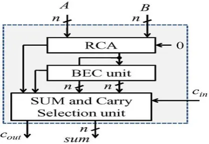
Fig. 1. (a) Conventional CSLA; n is the input operand bit-width. (b) The logic operations of the RCAA. SCG Unit Logic Expressions of the Conventional CSLA
The logic operations of the RCA are shown in split form, where HSG represent half-sum generation, HCG - half-carry generation, FSG - full-sum generation, and FCG - full-carry generation, respectively.As shown in Fig. 1(a), the SCG unit of the conventional CSLA [3] is composed of two n-bit RCAs, where n is the bit-width of adder. The logic operation of the n-bit RCA is performed in four stages in the given sequence: 1) half-sum generation (HSG) 2) half-carry generation (HCG) 3) full-sum generation (FSG) and 4) full carry generation (FCG). When two n-bit operands are added in the conventional CSLA, RCA-1 and RCA-2 generate n-bit sum (s0 and s1) and output carry ( 0
out
c
and 1out
c
) corresponding to input-carry (cin = 0 and cin = 1),respectively. Logic expressions of RCA-1 and RCA-2 of the Sum and Carry generator (SCG) unit of the n-bit CSLA are given as
0
0
( )
( )
( )
s i
A i
B i
c
00(i)
A(i).B(i)
(1a)0 0 0
1
( )
0( )
1(i 1)
s i
s i
c
(1b)0 0 0 0
1
( )
0( )
0( ). (i 1)
1c i
c i
s i c
c
out0(i)
c
10(n 1)
(1c)1
0
( )
( )
( )
s i
A i
B i
c
10(i)
A(i).B(i)
(2a)1 1 1
1
( )
0( )
1(i 1)
s i
s i
c
(2b)1 1 1 1
1
( )
0( )
0( ). (i 1)
1c i
c i
s i c
c
1out(i)
c
11(n 1)
(2c) wherec
10( 1)
0
,c
11( 1)
1
, and 0≤i≤n-1.As shown in (1a)–(1c) and (2a)–(2c), the logic expression of {
s
00(i)
,c
00(i)
} is identical to that of {s
10(i)
,c
10(i)
}. These redundant logic operations can be removed to have an optimized design for CSLA, in which the HSG and HCG of RCA-1 is shared to construct RCA-2. Based on this, [4] and [5] have used an add-one circuit design instead of RCA-2 in the CSLA, in which a BEC circuit is used [6] for the same purpose. Since the results shows that BEC-based CSLA offers the best area–delay– power efficiency among the existing CSLAs, we SCG unit of the BEC-based CSLA as well.B. SCG Unit Logic Expression of the BEC-Based CSLA
As shown in Fig. 2, the RCA calculates n-bit sum
s
10andc
out0 corresponding to cin = 0. The BEC unit receives0 1
s
and0
out
IJEDR1503116
International Journal of Engineering Development and Research (www.ijedr.org)3
Fig. 2. Structure of the BEC-based CSLA; here n is the input operand bit-width.The logic expressions of the n-bit BEC-based CSLA are given as
1 0
1
(0)
1(0)
s
s
c
11(0)
s
10(0)
(3a)1 0 1
1
( )
1( )
1(i 1)
s i
s i
c
(3b)1 0 1
1
( )
1( ). (i 1)
1c i
s i c
(3c)1 0 1
1
(n 1)
1(n 1)
out
c
c
c
(3d)for 1≤i≤n-1.
We can find from (1a)–(1c) and (3a)–(3d) that, in case of the BEC-based CSLA,
c
11depends ons
10, which otherwise has no dependence ons
10 in case of the conventional CSLA. Therefore the BEC method increases data dependence in CSLA. We have considered logic expressions of the conventional CSLA and made further study on the data dependence to find an optimized logic expression for the CSLA. It is interesting to know from (1a)–(1c) and (2a)–(2c) that logic expressions ofs
10 ands
11 are identical except the termsc
10 andc
11 since (s
10 =s
11 = s0). In addition, we find that0 1
c
andc
11 depends on {s0, c0, cin}, where c0 =
0 0
c
=
c
01. Sincec
00 andc
11 have no dependence ons
10 ands
11, the logic operation ofc
10 andc
11can be scheduled befores
10 ands
11, and the select unit can select one from the set (s
10 ands
11) for the final-sum of the CSLA. We analyze that a significant amount of logic resource is spent for calculating {s
10,s
11}, and Instead of an inefficient approach to reject one sum-word after the calculation, one can select the required carry word from the anticipated carry words { c0 and c1 } to calculate the final-sum. Theselected carry word is added with the half-sum (s0) to generate the final-sum (s). Using this design, one can have three advantages:
1) Calculation of
s
10 is avoided in the SCG unit 2) an n-bit select unit is required instead of the (n + 1) bit and 3) small output-carry delay. All these features result in an area, delay and energy-efficient design for the CSLA. We have eliminated all the redundant logic operations of (1a)–(1c) and (2a)–(2c) and rearranged logic expressions of the same based on their dependence. The proposed logic formulation for the CSLA is given as0
( )
( )
( )
s i
A i
B i
c i
0( )
A i B i
( ). ( )
(4a)c i
10( )
c i
0( )
s i c
0( ). (i 1)
10
for (c
10(0)
0
) (4b)c i
11( )
c i
0( )
s i c
0( ). (i 1)
11
for (c
11(0)
1
) (4c)c(i) =
c i
10( )
if (cin=0) (4d)c(i) =
c i
11( )
if (cin=1) (4e)cout =c(n-1) (4f)
s(0) =s0(0)
cin s(i) = s0(i)
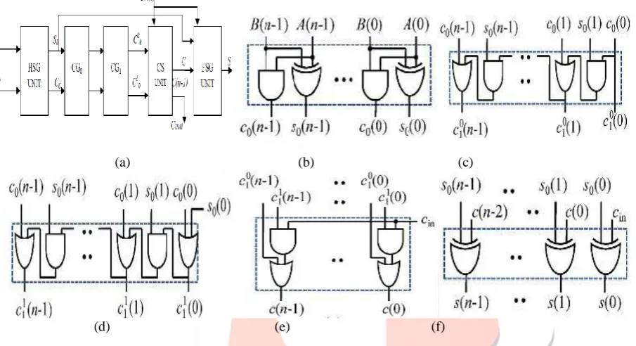
c(i-1) (4g)III. PROPOSED CSLA (ADDER) DESIGN
The proposed CSLA is based on the logic formulation given in (4a)–(4g), and its structure is shown in Fig. 3(a). It consists of one Half-sum generator (HSG) unit, one Full sum generator (FSG) unit, one Carry generator (CG) unit, and one Carry selector (CS) unit. The CG unit is composed of two CGs that is CG0 and CG1 corresponding to input-carry ‘0’ and ‘1’. The HSG receives two n-bit operands (A and B) and generate half-sum word s0 and half-carry word c0 of each n bits width. Both CG0 and CG1
receives s0 and c0 from the HSG unit and generate two individual n-bit full-carry words
0 1
IJEDR1503116
International Journal of Engineering Development and Research (www.ijedr.org)4
CG1 are optimized to take advantage of the fixed input-carry bits. The optimized designs of CG0 and CG1 are shown in Fig. 3(c) and (d), respectively. Here the CS unit selects one final carry word from the generated two carry words, available at its input line control signal cin. It selects0 1
c
when Cin = 0; otherwise, it selectsc
11. The CS unit can be implemented using an n-bit 2-to-l MUX. However, we find from the truth table of the CS unit that carry wordsc
10 andc
11follow a specific bit pattern. Ifc i
10( )
= ‘1’, then 11
( )
c i
= 1, irrespective of s0(i) and c0(i), for 0 ≤ i ≤ n − 1. This feature is used for logic optimization in the CS unit. Theoptimized design of the CS unit is shown in Fig. 3(e), which is composed of n AND–OR gates. The final carry word c is obtained from the CS unit. The MSB of c is sent to output as cout, and (n − 1) LSBs are XORed with (n − 1) MSBs of half-sum (s0) in the
FSG [shown in Fig. 3(f)] to obtain (n − 1) MSBs of final-sum (s). The LSB of s0 is XORed with cin to obtain the LSB of s.
(a) (b) (c)
(d) (e) (f)
Fig. 3. (a) Proposed CS adder design, where n is the input operand bit-width. Gate-level design of (b) the HSG (c) (CG0) for input-carry = 0. (d) (CG1) for input-carry =1. (e) The CS unit. (f) The final-sum generation (FSG) unit.
IV. PERFORMANCE COMPARISON
A. Area–Delay Estimation
We have considered all the gates to be made of 2-input AND, 2-input OR, and inverter (AOI) Logic. A 2-input XOR is composed of 2 AND gates, 1 OR gate, and 2
TABLE I
AREA, DELAY AND POWER OF AND, OR, AND NOT GATES
AND OR NOT
Area (um2) 13.30 13.30 6.65
Delay (ps) 174 200 29
Power (nw) 445.3 304.4 138.7
NOT gates. The area and delay of the 2-input AND gate, 2-input OR gate, and NOT gate (shown in Table I) are analyzed from the Cadence Tools using 180nm library. The area and delay of a design are calculated using the following relations:
A = a・ Na + r・ No + i・ Ni 5(a) T = na・ Ta + no・ To + ni・ Ti 5(b)
Where (Na, No, Ni) and (na, no, ni), respectively, represent the (AND, OR, NOT) gate counts of the total design and also its critical path. (a, r, i) and (Ta, To, Ti), represent the area and delay of one (AND, OR, NOT) gates respectively. We have calculated the (AOI) gate counts of each design for estimation of area and delay. Using 5(a) and 5(b), the area and delay of each design are calculated from the AOI gate counts (Na, No, Ni), (na, no, ni), and the cell details of Table I.
B. Single-Stage CSLA
IJEDR1503116
International Journal of Engineering Development and Research (www.ijedr.org)5
proposed n-bit CSLA and CSLAs of [6]–[8] and used AOI gate counts in 5(b) to find an expression for delay of final-sum and output-carry in the unit of Ti (NOT gate delay).C. Multistage CSLA (SQRT-CSLA)
SQRT-CSLA exploits the multipath carry propagation feature of the CSLA fully, it is composed of a chain of CSLAs. CSLAs of increasing bit size are used in the SQRT-CSLA to extract the maximum concurrence
TABLE II COMPARISION OF AREA, DELAY AND POWER OF PROPOSED AND EXISTING CSLAs
in the carry propagation path. Usually using the SQRT-CSLA design, the large-size adders can be implemented significantly, which gives less delay than a single-stage CSLA of same size.
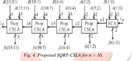
Fig. 4. Proposed SQRT-CSLA for n = 16.
However, carry propagation delay between the CSLA stages of present in SQRT-CSLA is critical for the overall adder delay. For area – delay efficient implementation of SQRT - CSLA the proposed CSLA design is more favorable than the existing CSLA designs, due to early generation of output-carry with multipath carry propagation feature. A 16-bit SQRT-CSLA design using the proposed CSLA is shown in Fig. 4, where the 2-bit RCA, 2-bit CSLA, 3-bit CSLA, 4-bit CSLA, and 5-bit CSLA are used. We have considered the cascaded configuration of (2-bit RCA and 2-, 3-, 4-, 6-, 7-, and 8-bit CSLAs) and (2-bit RCA and 2-, 3-, 4-, 6-, 7-, 8-, 9-, 11-, and 12-bit CSLAs), respectively, for the 32-bit SQRTCSLA and the 64-bit SQRT-CSLA to optimize adder delay. To demonstrate the advantage of the proposed CSLA design in SQRT-CSLA, we have estimated the area and delay of SQRTCSLA using the proposed CSLA design and the BEC-based CSLA of [6] and the CBL-based CSLA of [7] for bit-widths 16, 32, and 64 using Tables I, II, and (5a) and (5b). The estimated values are listed in Table III for comparison.
D. ASIC Synthesis Results
We have coded the SQRT-CSLA in Verilog using the proposed CSLA design and existing CSLA designs of conventional and BEC based for bit-widths 16, 32 and 64. All the designs are synthesized in the Cadence Encounter tool using the 180nm CMOS library. The area, delay and power reported for comparison in Table.
V. CONCLUSION
We analyze the logic operations involved in the conventional (including BEC-based) CSLAs. We study the data dependence and identified redundant logic operations. We eliminate all the redundant logic operations of the conventional CSLA and proposed a new logic formulation for the same. In the proposed scheme, Carry words corresponding to input-carry ‘0’ and ‘1’ generated by the CSLA follow a specific bit pattern, which is used for logic optimization
TABLE III
COMPARISION OF APPLICATION-SPECIFIC INTEGRATED CIRCUIT (ASIC) SYNTHESISE RESULTS USING CADENCE 180-nm CMOS LIBRARY OF THE PROPOSED AND EXISTING CSLAs
Design Width (n)
Area (um2)
Delay (ns)
Power (uW)
SQRT- 16 2282 3.10 168.957
Design Width (n)
Area (um2)
Delay (ns)
ADP (um2us)
Power (uW) CONV
8 1284 2.96 3.80 100.625
16 2615 5.74 15.01 217.903
32 5276 11.31 59.67 443.795 CSLA
[BEC]
8 1044 3.18 3.32 73.522
16 2108 5.96 12.56 156.401
32 4238 11.53 48.86 315.892 Prop.
8 589 2.56 1.51 30.128
16 1217 4.78 5.82 64.669
IJEDR1503116
International Journal of Engineering Development and Research (www.ijedr.org)6
CSLA(CONV)
32 4850 5.01 374.808
64 10032 8.48 792.601
SQRT-CSLA[B EC]
16 1923 3.01 137.544
32 4012 4.83 287.970
64 3210 8.16 596.315
Proposed SQRT-CSLA
16 1141 4.97 87.234
32 2338 8.81 138.358
64 4750 16.97 252.391
of the CS unit. Fixed input bits of the CG unit are also used for logic optimization. Based on this, an optimized design for CS and CG units are obtained. Using these optimized logic units. The proposed CSLA design involves significantly less area and delay compared to BEC-based CSLA. Due to the small carry output delay, the proposed CSLA design is a good candidate for the SQRT adder. The ASIC synthesis report shows that the proposed SQRT-CSLA involves 48% less ADP and consumes 50% less energy than the existing BEC-based SQRT-CSLA design, on an average, for different bit-widths.
REFERENCES
[1] K. K. Parhi, VLSI Digital Signal Processing. New York, NY, USA:Wiley, 1998.
[2] A. P. Chandrakasan, N. Verma, and D. C. Daly, “Ultralow-power electronics for biomedical applications,” Annu. Rev. Biomed. Eng., vol. 10, pp. 247– 274, Aug. 2008.
[3] O. J. Bedrij, “Carry-select adder,” IRE Trans. Electron. Comput., vol. EC-11, no. 3, pp. 340–344, Jun. 1962.
[4] Y. Kim and L.-S. Kim, “64-bit carry select adder with reduced area,” Electron. Lett., vol. 37, no. 10, pp. 614-615, May 2001. [5] Y. He, C. H. Chang, and J. Gu, “An area-efficient 64-bit square root carry select adder for low power application,” in Proc. IEEE Int. Symp. Circuits Syst., 2005, vol. 4, pp. 4082–4085.
[6] B. Ramkumar and H.M. Kittur, “Low-power and area-efficient carry-select adder,” IEEE Trans. Very Large Scale Integr. (VLSI) Syst., vol. 20, no. 2,pp. 371–375, Feb. 2012.
[7] I.-C. Wey, C.-C. Ho, Y.-S. Lin, and C.C. Peng, “An area-efficient carry select adder design by sharing the common Boolean logic term,” in Proc.IMECS, 2012, pp. 1–4.
[8] S.Manju and V. Sornagopal, “An efficient SQRT architecture of carry select adder design by common Boolean logic,” in Proc. VLSI ICEVENT, 2013,pp. 1–5.
[9] B. Parhami, Computer Arithmetic: Algorithms and Hardware Designs,2nd ed. New York, NY, USA: Oxford Univ.Press, 2010.
Authors
Gutlapalli Venkatrao working as Asst.Professor in Geethanjali college of Engineering & Technology Cheryal, HYD and received Masters in VLSI system design at Anurag Group of Institutions formerly known CVSR College of Engineering HYD, AP, India in 2014 and B.Tech degree in ECE from AVCR (JNTU), AP, India, in 2011. His current research interests include Digital Design, Design for Testability (DFT) and Low Power VLSI