A Reconfigurable Low Noise Amplifier for
a Multi-standard Receiver
A Thesis
SUBMITTED IN FULFILMENT OF THE REQUIREMENTS FOR THE DEGREE OF
DOCTOR OF PHILOSOPY
By
Mohd Tafir Mustaffa
To
School of Engineering & Science
Faculty of Health, Engineering and Science
Victoria University
Australia
Declaration of Originality
I, Mohd Tafir Mustaffa, declare that the PhD thesis entitled “A Reconfigurable Low
Noise Amplifier for a Multi-standard Receiver” is no more than 100,000 words in
length including quotes and exclusive of tables, figures, appendices, bibliography,
references and footnotes. This thesis contains no material that has been submitted
previously, in whole or in part, for the award of any other academic degree or
diploma. Except where otherwise indicated, this thesis is my own work.
Mohd Tafir Mustaffa
To my wonderful wife Khairunnisa Baruddin
and
ABSTRACT
Mobile devices are widely used for a vast range of applications such as mobile phones,
personal digital assistant, personal computers, video games console, etc. However, the
performance of these devices is restricted by the support of the network and the mobile
functionality and efficiency. Current applications require high data rates and global
mobility which can be satisfied with the co-existence and handover between newly
developed third generation (3G) or Universal Mobile Telecommunication System
(UMTS) standard and current second generation (2G) standards including: Global
Standards for Mobile (GSM), Digital Cellular System (DCS), and Personal
Communication Systems (PCS). Therefore, recent research in wireless communication
has shifted towards achieving a multi-standard terminal, which can support efficiently
multiple standards including GSM/DCS/PCS/3G.
References show that currently available multi-standard receivers employ parallel
architecture to accommodate multiple standards. This option, however, is bulky, costly,
complex, and consumes relatively high power. To address these limitations, current
research trend is to merge the parallel paths into a single path wireless receiver.
Literature review shows that currently available low noise amplifier (LNA) as part of this
receiver, only support combination of a few mobile communication standards.
Therefore, there is a need for a new LNA architecture that could support most of the 2G
In this research, the aim is to design and implement a new LNA for a multi-standard
mobile receiver based on reconfigurability concept. This research was carried out in two
major parts. The first part is to design and implement wide band standard
multi-band LNAs for two multi-bands of interest (lower frequency multi-band – 800 to 1000 MHz and
upper frequency band – 1800 to 2200 MHz). These two bands should cover most of the
2G and 3G standards currently in use worldwide. In this work, the design of LNA based
on IDCS topology using wide band approach has been investigated, designed,
implemented and approved by means of simulations, and measurement of fabricated
ICs. The second part of this research, to develop a single reconfigurable multi-standard
multi-band LNA is based on the design of the multi-standard multi-band LNAs. This LNA
has the capability to function in two modes of operation, either at lower band or upper
band of the 2G or 3G standards.
The significance of this research is to respond to the industries need of multi-standard
multi-band LNA with simple architecture. This LNA is less complex, more power efficient
and cost effective compared to the parallel architecture in the design of the
multi-standard RF receiver architecture. Therefore, the proposed reconfigurable LNA
provides access to functions such as voice calls, video calls, multimedia messaging,
ACKNOWLEDGEMENTS
First and foremost, I would like to express my special appreciation to my supervisor
Associate Professor Dr Aladin Zayegh for his teaching, guidance, support, assistance
and encouragement during this research. The opportunities and learning experiences
he has given me are much appreciated. The experience at Victoria University has been
especially rewarding and helpful for my future career because of his support, not only in
the research work but also in many other aspects. I would also like to show my
appreciation to my co-supervisors, Dr Ronny Veljanovski and Associate Professor
Aleksandar Stojcevski for their timely advice and support throughout this research.
I would like to express my thanks to RMIC group from Universiti Sains Malaysia (USM),
especially Dr Tun Zainal Azni Zulkifli, for their support, advice and teaching throughout
this research. I cannot forget the facilities provided by CEDEC (Collaborative
µElectronic Design Excellence Centre) of USM for fabrication and measurement of my
LNAs, without which my research would not reach this level. Special thanks to
Associate Professor Dr Othman, director of CEDEC for that opportunity. My thanks also
go to Silterra Malaysia for the design kit and access to fabrication through CEDEC.
I also would like to thank my colleagues at the School of Electrical Engineering for their
valuable support. In particular, I would like to thank, Amanullah Maung Than Oo,
Jaideep Chandran, Nikhil Joglekar and other friends in room G218, School of
Engineering and Science.
Above all, I would like to give special thanks and great appreciations to my wonderful
wife Khairunnisa Baruddin and my family in Malaysia for their love, patience,
understandings, sacrifices, prayers and encouragements during the research and thesis
LIST OF ABBREVIATIONS
2G Second Generation
3G Third Generation
3GPP 3rd Generation Partnership Project
ADS Advanced Design System
BER Bit Error Rate
BiCMOS Bipolar CMOS
BPF Band Pass Filter
CEDEC Collaborative µElectronic Design Excellence Centre
CG Common Gate
CMOS Complementary Metal Oxide Semiconductor
CNR Carrier to Noise Ratio
CS Common Source
DCR Direct Conversion Receiver
DCS Digital Cellular System
drc design rule check
DUT Device Under Test
EGSM Enhanced-GSM
ETSI European Telecommunication Standards Institute
GMSK Gaussian Minimum Shift Keying
GPS Global Positioning System
GSM Global Standards for Mobile
IDCS Inductively-Degenerated Common Source
IF Intermediate Frequency
IP2 Second Order Intercept Point
IP3 Third Order Intercept Point
LNA Low Noise Amplifier
LO Local Oscillator
lvs layout versus schematic
MEMS Micro Electro Mechanical System
NCSU North Carolina State University
NF Noise Figure
NQS Non-Quasi Static
PCS Personal Communication Systems
pex parasitic extraction
QPSK Quadrature Phase-Shift Keying
RF Radio Frequency
RFIC Radio Frequency Integrated Circuit
SiGe Silicon Germanium
TI Texas Instrument
TOI Third Order Intercept Point
UMTS Universal Mobile Telecommunication System
USM Universiti Sains Malaysia
VCO Voltage Controlled Oscillator
WCDMA Wide Code Division Multiple Access
TABLE OF CONTENTS
ABSTRACT ii
ACKNOWLEDGEMENTS iv
LIST OF ABBREVIATIONS vi
TABLE OF CONTENTS ix
LIST OF FIGURES xiv
LIST OF TABLES xx
LIST OF PUBLICATIONS xxii
CHAPTER 1: THESIS OVERVIEW 1.0 Introduction 1
1.1 Research methodologies and techniques 6
1.2 Organisation of the Thesis 9
1.3 Originality of the Thesis 10
CHAPTER 2: LITERATURE REVIEW 2.0 Introduction 12
2.1 Multi-standard RF systems 14
2.1.1 RF standards 14
2.1.2 RF receiver architectures 21
2.1.3 The development of RF receiver architectures 27
2.2.1 Recent developments of reconfigurable
multi-standard system 33
2.2.2 Recent developments of reconfigurable multi-standard LNA 37
2.3 Conclusion 40
CHAPTER 3: LNA THEORIES AND DESIGNS 3.0 Introduction 42
3.1 LNA theories 43
3.1.1 Impedance matching 44
3.1.2 Noise sources in CMOS 47
3.1.3 S-parameters 55
3.1.4 Linearity 56
3.2 Multi-standard multi-band LNA 57
3.2.1 Multi-standard LNA 57
3.2.2 Multi-standard LNA for wide band receiver system 59
3.2.3 Multi-standard multi-band LNA designs using wide band approach 62
3.3 Multi-standard multi-band LNA designs 64
3.3.1 Multi-standard multi-band LNA design flow 64
3.3.2 Multi-standard multi-band LNA designs – 2 GHz with buffer 66
3.3.3 Multi-standard multi-band LNA designs –
0.9 GHz with no buffer 74
3.3.4 Multi-standard multi-band LNA design –
2 GHz with no buffer 80
3.4 Conclusion 82
CHAPTER 4: RESULTS AND DISCUSSION
4.0 Introduction 84
4.1 Pre-layout simulation results 85
4.1.1 Multi-standard multi-band LNA designs –
2 GHz with buffer 85
4.1.2 Multi-standard multi-band LNA designs –
0.9 GHz with no buffer 94
4.1.3 Multi-standard multi-band LNA design –
2 GHz with no buffer 102
4.2 Post-layout simulation results 106
4.2.1 Multi-standard multi-band LNA2 design –
2 GHz with buffer 106
4.2.2 Multi-standard multi-band LNA4 design –
0.9 GHz with no buffer 109
4.2.3 Multi-standard multi-band LNA5 design –
2 GHz with no buffer 112
4.4 Conclusion 120
CHAPTER 5: MEASUREMENT RESULTS OF THE FABRICATED LNAs
5.0 Introduction 121
5.1 Measurement setup 122
5.2 Measurement results of the fabricated LNAs 123
5.2.1 Multi-standard multi-band LNA2 IC measurement –
2 GHz with buffer 123
5.2.2 Multi-standard multi-band LNA4 IC measurement –
0.9 GHz with no buffer 132
5.2.3 Multi-standard multi-band LNA5 IC measurement –
2 GHz with no buffer 141
5.3 Discussion of the results 153
5.4 Conclusion 157
CHAPTER 6: RECONFIGURABLE MULTI-STANDARD MULTI-BAND LNA
6.0 Introduction 159
6.1 Design and implementation of reconfigurable multi-standard
multi-band LNA 160
6.1.1 Design consideration 160
6.1.2 A reconfigurable multi-standard multi-band LNA 162
6.1.3 Circuit implementation of reconfigurable multi-standard
6.2 Simulation results 172
6.3 Discussion of the results 182
6.4 Conclusion 184
CHAPTER 7: CONCLUSIONS AND RECOMMENDATIONS FOR FUTURE WORK
7.0 Introduction 186
7.1 Summary and achievements of the research 187
7.2 Recommendations for future work 190
REFERENCES 192
APPENDIX A: THE REFLECTION COEFFICIENT OF THE LOADED TRASMISSION
LINE 212
APPENDIX B: THE NON-QUASI STATIC EFFECT OF CMOS TRANSISTOR 214
APPENDIX C: PASSIVE COMPONENTS OF THE DESIGN KIT 216
APPENDIX D: S-PARAMETERS OF THE LNA 218
LIST OF FIGURES
Figure 1.1: 3G phone with various applications [1] 2
Figure 2.1: Superheterodyne architecture [48] 22
Figure 2.2: Homodyne architecture [46] 24
Figure 2.3: Effect of even-order distortion [51] 26
Figure 2.4: Parallel DCR architecture for multi-standard mobile as in [20] 28
Figure 2.5: QUALCOMM chip solution (redrawn partly) [10] 29
Figure 2.6: Superheterodyne receiver as in [55] 30
Figure 2.7: Superheterodyne receiver as in [56] 31
Figure 2.9: Reconfigurable receiver architecture as in [65] 34
Figure 2.10: 2-6 GHz multi-standard receiver architecture [67] 34
Figure 2.11: Proposed receiverarchitecture 36
Figure 2.12: Multiband LNAarchitecture [68] 38
Figure 2.13: Dual-standard LNA as in [69] 39
Figure 3.1: Condition for impedance match 44
Figure 3.2: Inductive source degeneration 45
Figure 3.3: Standard CMOS noise model representing thermal noise [25] 47
Figure 3.4: IDCS circuit for input stage noise calculations [25] 48
Figure 3.5: Standard CMOS noise model representing induced gate noise [25] 50
Figure 3.7: Wide band IDCS LNA1 [85] 66
Figure 3.8: Wide band IDCS LNA2 [88] 72
Figure 3.9: Layout of CMOS LNA2 with GSG pad and DCQ pad for dc supply and biasing voltage [88] 74
Figure 3.10: Wide band LNA3 [89] 75
Figure 3.11: Wide band LNA4 [90] 78
Figure 3.12: Layout of CMOS LNA4 with GSG pad and DCQ pad for dc supply and biasing voltage [90] 79
Figure 3.13: Wide band LNA5 [91] 81
Figure 3.14: Layout of CMOS LNA5 with GSG pad and DCQ pad for dc supply and biasing voltage [91] 82
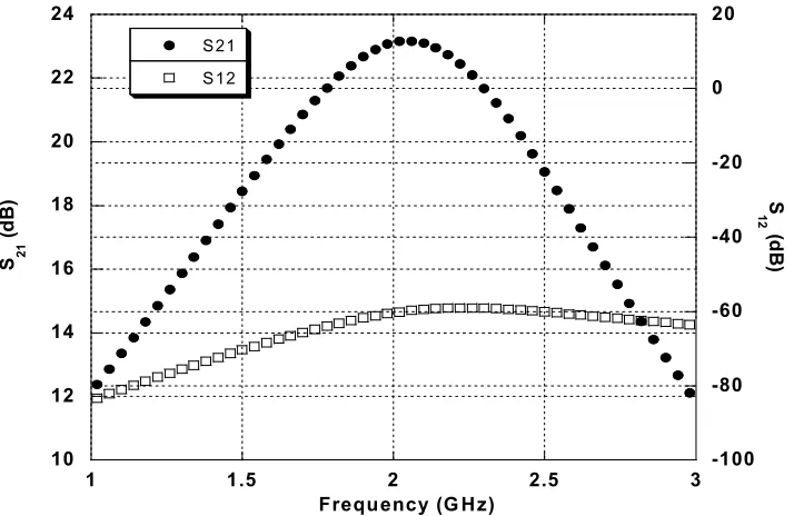
Figure 4.1: Forward gain and reverse isolation of LNA1 86
Figure 4.2: Input and output return losses of LNA1 86
Figure 4.3: Noise figure of LNA1 87
Figure 4.4: IIP3 of LNA1 88
Figure 4.5: P1dB of LNA1 89
Figure 4.6: Forward gain and reverse isolation of LNA2 90
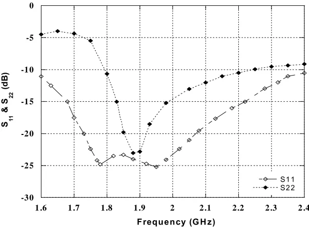
Figure 4.7: Input and output return losses of LNA2: 22
S
(a) not optimised for linearity,S
22 (b) optimised for linearity 91Figure 4.8: Noise figure of LNA2 92
Figure 4.9: IIP3 of LNA2 93
Figure 4.10: P1dB of LNA2 93
Figure 4.12: Input and output return losses of LNA3 95
Figure 4.13: Noise figure of LNA3 96
Figure 4.14: IIP3 of LNA3 97
Figure 4.15: P1dB of LNA3 97
Figure 4.16: Forward gain and reverse isolation of LNA4 99
Figure 4.17: Input and output return losses of LNA4 99
Figure 4.18: Noise figure of LNA4 100
Figure 4.19: IIP3 of LNA4 101
Figure 4.20: P1dB of LNA4 101
Figure 4.21: Forward gain and reverse isolation of LNA5 103
Figure 4.22: Input and output return losses of LNA5 104
Figure 4.23: Noise figure of LNA5 104
Figure 4.24: IIP3 of LNA5 105
Figure 4.25: P1dB of LNA5 106
Figure 4.26: Post-layout forward gain and reverse isolation of LNA2 107
Figure 4.27: Post-layout input and output return losses of LNA2 108
Figure 4.28: Post-layout noise figure of LNA2 109
Figure 4.29: Post-layout forward gain and reverse isolation of LNA4 110
Figure 4.30: Post-layout input and output return losses of LNA4 111
Figure 4.31: Post-layout noise figure of LNA4 112
Figure 4.32: Post-layout forward gain and reverse isolation of LNA5 114
Figure 4.33: Post-layout input and output return losses of LNA5 114
Figure 4.35: Noise figure simulation with different values of LS 118
Figure 4.36: Output return loss (S22): fix R1 but different values of L1 119
Figure 4.37: Output return loss (S22): fix L1 but different values ofR1 119
Figure 5.1: Measurement strategy [95] 122
Figure 5.2: Measured Iload versus Idc 124
Figure 5.3: Forward gain and reverse isolation of LNA2 with Idc =1mA 125
Figure 5.4: Forward gain and reverse isolation of LNA2 with Idc =5mA 126
Figure 5.5: Forward gain and reverse isolation of LNA2 with Idc =10mA 126
Figure 5.6: Input and output return losses of the LNA2 with Idc=1mA 128
Figure 5.7: Input and output return losses of the LNA2 with Idc=5mA 128
Figure 5.8: Input and output return losses of the LNA2 with Idc=10mA 129
Figure 5.9: IIP3of LNA2 with Idc=1mA 131
Figure 5.10: P1dB of LNA5 with Idc=1mA 131
Figure 5.11: Measured Iload versus VIN (bias) for LNA4 132
Figure 5.12: Forward gain and reverse isolation of LNA4 with 0.7V bias 134
Figure 5.13: Forward gain and reverse isolation of LNA4 with 0.65V bias 134
Figure 5.14: Forward gain and reverse isolation of LNA4 with 0.6V bias 135
Figure 5.15: Input and output return losses of the LNA4 with 0.7V bias 137
Figure 5.16: Input and output return losses of the LNA4 with 0.65V bias 137
Figure 5.17: Input and output return losses of the LNA4 with 0.6V bias 138
Figure 5.18: IIP3of LNA4 with 0.7V bias 139
Figure 5.19: P1dB of LNA4 with 0.7V bias 140
Figure 5.21: Forward gain and reverse isolation of LNA5 with 0.7V bias 142
Figure 5.22: Forward gain and reverse isolation of LNA5 with 0.65V bias 143
Figure 5.23: Forward gain and reverse isolation of LNA5 with 0.6V bias 143
Figure 5.24: Input and output return losses of the LNA5 with 0.7V bias 144
Figure 5.25: Input and output return losses of the LNA5 with 0.65V bias 145
Figure 5.26: Input and output return losses of the LNA5 with 0.6V bias 146
Figure 5.27: IIP3of LNA5 with 0.7V bias 148
Figure 5.28: P1dB of LNA5 with 0.7V bias 148
Figure 5.29: IIP3 of LNA5 with 0.65V bias 149
Figure 5.30: P1dB of LNA5 with 0.65V bias 149
Figure 5.31: IIP3 of LNA5 with 0.6V bias 150
Figure 5.32: P1dB of LNA5 with 0.6V bias 150
Figure 5.33: Die photograph of LNA2 151
Figure 5.34: Die photograph of LNA4 152
Figure 5.35: Die photograph of LNA5 152
Figure 6.1: Circuit diagram of a reconfigurable multi-standard multi-band LNA 163
Figure 6.2: Revised IDCS small-signal model for reconfigurable LNA 163
Figure 6.3: Complete circuit implementation of a reconfigurable LNA 171
Figure 6.4: Forward gain and reverse isolation of reconfigurable LNA for upper band at 2GHz 172
Figure 6.5: Forward gain and reverse isolation of reconfigurable LNA for lower band at 0.9GHz 173
for upper band at 2GHz 174
Figure 6.7: Input and output return losses of reconfigurable LNA for lower band at 0.9GHz 175
Figure 6.8: Noise figure of reconfigurable LNA for upper band at 2 GHz 176
Figure 6.9: Noise figure of reconfigurable LNA for lower band at 0.9 GHz 177
Figure 6.10: IIP3 for upper band at 2 GHz with Iload=10.45 mA 178
Figure 6.11: IIP3 for upper band at 0.9 GHz with Iload=14.7 mA 178
Figure 6.12: IIP3 for upper band at 2 GHz with Iload=8.75 mA 179
Figure 6.13: IIP3 for upper band at 0.9 GHz with Iload=12.43 mA 179
Figure 6.14: P1dB for upper band at 2 GHz with Iload= 10.45 mA 180
Figure 6.15: P1dB for upper band at 0.9 GHz with Iload= 14.7 mA 180
Figure 6.16: P1dB for upper band at 2 GHz with Iload= 8.75 mA 181
Figure 6.17: P1dB for upper band at 0.9 GHz with Iload = 12.43 mA 181
Figure A.1: Transmitted and reflected voltages and currents [93] 212
Figure B.1: A first order non-quasi static small-signal model for transistors operating in strong inversion: (a) valid in both linear and saturation region (b) valid in saturation region only [93] 214
Figure D.1: S-parameters representation of a two-port 218
LIST OF TABLES
Table 2.1: Frequency allocation for GSM systems [2-4] 16
Table 2.2: Frequency allocation for UMTS systems [7] 16
Table 2.3: Signal characteristics for GSM/3G systems 17
Table 2.4: Receiver specifications for GSM/3G systems and the proposed
specifications for multi-standard system [46-48] 19
Table 2.5: Ideal LNA specifications proposed for multi-standard
multi-band system 20
Table 2.6: Typical LNA specifications proposed for multi-standard
multi-band system 20
Table 3.1: Component values for LNA1 71
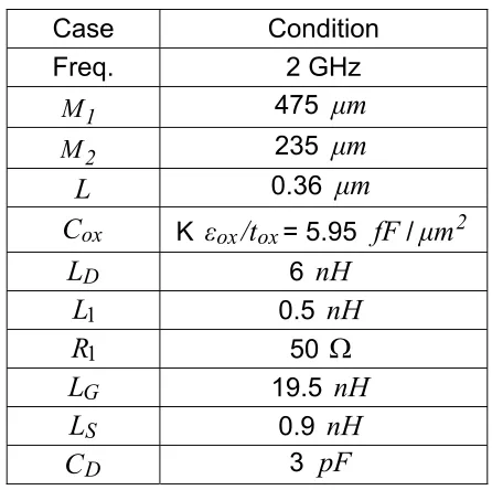
Table 3.2: Component values for LNA2 73
Table 3.3: Component values for LNA3 77
Table 3.4: Component values for LNA4 79
Table 3.5: Component values for LNA5 81
Table 4.1: Performance summary of the wide band LNAs 116
Table 5.1: Performance summary of the measurement results for
chip 2 of the LNA2 129
Table 5.2: Performance summary of the measurement results for
chip 3 of the LNA2 130
Table 5.3: Linearity performance summary of the other current bias for LNA2 132
Table 5.4: Performance summary of the measurement results for
Table 5.5: Performance summary of the measurement results for
chip 3 of the LNA4 139
Table 5.6: Linearity performance summary of the other chip for LNA4 140
Table 5.7: Performance summary of the measurement results for
chip 2 of the LNA5 146
Table 5.8: Performance summary of the measurement results for
chip 3 of the LNA5 147
Table 5.9: Linearity performance summary of the other chips for LNA5 151
Table 5.10: Performance summary of the wide band LNAs 155
Table 5.11: Achieved bandwidths of the wide band LNAs 156
Table 5.12: Comparison with other publications 157
Table 6.1: Component values for reconfigurable multi-standard multi-band LNA 171
Table 6.2: Performance summary of the reconfigurable LNA
versus wide band LNAs 183
LIST OF PUBLICATIONS
Journals
1. Mustaffa M.T, Zayegh A, Veljanovski R., Stojcevski A., and Zulkifli T.Z.A.,
“CMOS Low Noise Amplifier for wideband mobile receiver,” Accepted for
publication in Journal of the Advancement of Modelling and Simulation
Techniques (AMSE), France, in 2008.
Conference papers
1. Mustaffa M.T, Zayegh A, Veljanovski R., Stojcevski A., and Zulkifli T.Z.A., “0.18
µm Fully Integrated 900 MHz CMOS LNA with Input and Output On-chip
matching for Multi-standard Mobile Receiver,” Proceedings of IEEE International
Conference on Microelectronics, 14-17 December 2008, Sharjah, UAE.
2. Mustaffa M.T, Zayegh A, Veljanovski R., Stojcevski A., and Zulkifli T.Z.A., “Fully
Integrated 2-GHz LNA with On-chip matching for Multi-standard Mobile Receiver
using 0.18 µm CMOS Technology,” Proceedings of IEEE TENCON International
Conference, 18-21 November 2008, Hyderabad, India.
3. Mustaffa M.T, Zayegh A, Veljanovski R. and Stojcevski A., “A 0.8 GHz to 1 GHz
0.25 μm CMOS Low Noise Amplifier for Multi-standard Receiver,” Proceedings of
IEEE International Conference on Intelligent & Advanced Systems, 25-28
4. Mustaffa M.T, Zayegh A, Veljanovski R. and Stojcevski A., “A 1.8 GHz to 2.1
GHz 0.25 μm CMOS Wideband LNA for a Multi-standard Mobile Receiver,”
Proceedings of IEEE International Symposium on Integrated Circuits (ISIC),
26-28 September 2007, Orchard Hotel, Singapore.
5. Mustaffa M.T, Zayegh A, Veljanovski R. and Stojcevski A., “Optimised Low Noise
Amplifier for Multi-standard Receiver Architecture,” Proceedings of International
Conference on Advanced Technologies in Telecommunications and Control
CHAPTER 1:
THESIS OVERVIEW
1.0 Introduction
The increasing demands of higher data transfer rates and global mobility in current
wireless communication environment has led to the development of the Third
Generation (3G) mobile communication standard. Nowadays, many small and large
operators, serving both developed and emerging markets, are already reaping the
benefits of 3G technologies. As of January 2008, there were 435 3G operators (service
providers) worldwide, with more than 560 million subscribers in 143 countries [1].
The 3G wireless communication system provides voice communication together with
multimedia communication such as video, internet, real TV, live cast, etc. as is
represented in Figure 1.1. It supports Universal Mobile Telecommunication System
(UMTS) or Wide Code Division Multiple Access (WCDMA) standard and also provides a
backward compatibility with Second Generation (2G) systems [2-9]. Typical standards
currently being used for 2G systems are: Global Standard for Mobile (GSM900) and
Digital Cellular System (DCS1800) and Personal Communication System (PCS1900)
[2-9]. In other words, the new 3G phone is a representation of new wireless trend
TV Voice
Wallet
Pager Newspaper
PC
Photo Album Camera
Rolodex
GPS Device FM Radio Camcorder
Glucometer
Bar Scanner
MP3 Player
Game Controls Walkie-Talkie
PDA
Figure 1.1: 3G phone with various applications [1]
Due to increasing demand on the 3G mobile, QUALCOMM, Texas Instrument (TI), etc.
(companies that provide chipset solution for 3G systems) have come up with systems
using parallel architecture to cover various standards [10-12]. This concept of parallel
architecture maybe originated from various radio frequency (RF) standard
multi-band parallel systems which were developed over the past years as shown in
references [13-20]. Unfortunately, this type of implementation is very area inefficient,
different systems or devices. In other words, consumers are paying additional cost for
the added complexity of such a system. In addition, with the complex functionality
(e-mail, video call, etc.), the issue of a shorter battery life of a 3G phone compared to
well-known GSM mobile is quite common, as the battery might go flat within just one day, or
even worse, within hours if heavy usage of the 3G mobile took place.
Having mentioned the problems with the current solutions, it is impractical in the future
to adapt such implementation in designing the multi-standard multi-band mobile device,
as more and more 3G wireless standards are emerging [8-9]. With these emerging
standards, wireless mobile system is more complex and the system integration is
virtually impossible or hard to be realised and impractical. Therefore, the search for a
new system or architecture seems to be evident. Solutions to these problems are
possible by introducing a new architecture with reconfigurability features that should be
able to support most of the available standards [8-9].
With respect to this approach, it is possible to develop a new architecture that can cover
various standards with just one single terminal, compared to the current architecture
that uses a single terminal for each single standard. For instance, as GSM comprise
standards that use multiple bands in the lower frequency bands: 850 and 900 MHz and
the upper frequency bands: 1800 and 1900 MHz [2-9], two new circuits (in particular,
low noise amplifier (LNA) as it is the main work of this research) could be designed to
For the reconfigurability feature, the principle refers to the ability of the circuit to perform
changes in function due to the operating environment by selecting certain section of the
circuit at one time to operate, while the other sections can be switched off to reduce
power consumption. Referring to this research work, reconfigurable means to modify
the hardware structure to respond to the two major bands of interest (i.e. lower and
upper frequency band regimes) depending on the availability of the mobile
communication systems (GSM or 3G).
To design such a new architecture with reconfigurability feature, a platform (i.e. mobile
receiver system) is required. Since LNA is part of the receiver system, a good receiver
architecture that is suitable for multi-standard multi-band implementation is needed.
From the literature, direct conversion receiver (DCR) architecture is believed to be the
most suitable architecture for single-chip multi-standard multi-band mobile receiver
[18-19]. This is because of its advantages such as simple circuit architecture and less
off-chip components, leading to low power consumption with possible integration as a
single-chip radio [18-24].
In DCR architecture, RF signal is amplified and converted to baseband signal in only
one stage. Typically, DCR architecture consists of a Band Pass Filter (BPF), a LNA, a
mixer, a voltage controlled oscillator (VCO), etc. In DCR architecture, LNA is considered
as the most important block, as it directly affects the performance of the receiver. It
process the signal and at the same time offers low noise figure (NF) and high linearity to
increase the accuracy and performance of the system.
For years, LNA has been the topic of research due to its different performance
requirements for different standards [25-33]. Gain, NF, linearity, and low power
consumption are the major specifications in the design of LNA, and the most important
parameter is NF. To achieve a low NF, common source stage with inductive
degeneration showed the best noise performance with good gain and sufficient linearity
with a trade-off with power consumption [25-27]. Several techniques and methods have
been tried in order to produce a LNA with low NF [25-33], but, most of these methods
and techniques are limited to the single standards only.
However, due to the high demand of multi-standard device, the trend of LNA design
seems to move from single-standard to multi-standard LNA, with different methods and
topologies as appears in literatures [34-39]. The most popular technology nowadays
used to implement LNA is complementary metal oxide semiconductor (CMOS)
technology which offers low power consumption and low cost solution [25-30].
In this research, an attempt to investigate and to develop effective ways of
implementing architecture to support multi-standard multi-band personal wireless
1.1 Research methodologies and techniques
The aim of this research is to design and implement a low power, low noise,
reconfigurable LNA using CMOS technology for a multi-standard multi-band mobile
receiver based on industry-standard. The design and implementation of the LNA will
provide the reconfigurable feature which allows the selection of different standards such
as: GSM and 3G. In addition, the design of reconfigurable LNA was based on
industry-standard process technologies and libraries such as that from MOSIS and Silterra which
is similar to the technologies used by major microelectronics companies such as Intel,
IBM and Freescale. Design, implementation, simulation and measurement were carried
out using leading design tools and instruments: Agilent Design Suite (ADS), Cadence
Design Suite (Spectre RF), Mentor Graphics (Calibre) and Agilent’s instruments etc.
The details of proposed methodology and techniques to achieve the requirements of
this research project are as follows:
1.2.1 Analysis of the currently available systems / Literature review
This initial stage of the research program involved searching the state of art in the field
of multi-standard receiver systems especially the receiver architectures. One important
aspect of this research is to understand the wireless receiver architectures and their
requirements. The system level standards for GSM, DCS, PCS and UMTS have been
see the relation between receiver specifications and components specifications,
especially LNA, as it is the main focus of this research. This step of analysis in the
research provides the optimum LNA specifications, extracted from the receiver’s
specifications, which will be used as guideline for designing the LNA at the later stage of
the research.
1.2.2 Design and implementation of wide band CMOS LNAs for multi-standard
receiver
Based on the extracted specifications from receiver standards, two wide band CMOS
LNAs were designed and implemented for multi-standard receiver. These LNAs were
designed for two bands of interest which are lower frequency band (800 to 1000 MHz)
and upper frequency band (1800 to 2200 MHz) respectively. To achieve this
implementation, various CMOS LNA’s topologies or methods were reviewed and
studied. Wide band multi-standard multi-band LNAs were designed, simulated and
implemented using the Cadence design suite based on 0.25 μm industry-standard
process technology and library from MOSIS. At this stage, only ideal passive
components used. Subsequently, the process of designing continued with the design
and implementation of LNAs using more realistic technology and library provided by
1.2.3 Layout implementation and fabrication of wide band CMOS LNAs for
multi-standard receiver.
After the wide band LNAs was successfully designed and simulated, the research
development moved forward with the layout implementation and fabrication. In this
stage, post-layout simulations were carried out to verify the validity of circuit design; the
layout has been implemented using 0.18 µm technology by means of Cadence tools,
while Calibre tools were utilised to obtain post-layout design rule check (drc), layout
versus schematic (lvs) and parasitic extraction (pex). Based on the successful results
from the simulation, the layouts have been submitted for fabrication.
1.2.4 Test and measurement of the fabricated LNAs
This step has been carried out at the Collaborative µElectronic Design Excellence
Centre (CEDEC) at Universiti Sains Malaysia (USM) using a leading measurement
instruments available at the centre. The measurement has been carried out to measure
the parameters of the fabricated LNAs: s-parameters (gain, input and output return
losses and reverse isolation) and linearity parameters: third order intercept point (TOI)
and compression point (P1dB).
1.2.5 Design and implementation of reconfigurable multi-standard multi-band
LNA
This step involved the design and implementation of a single reconfigurable
multi-standard multi-band LNA for mobile receiver. The reconfigurable LNA has been
designed in such a way that, it has the capability to support two bands of interest which
are lower frequency band (800 to 1000 MHz) and upper frequency band (1800 to 2200
MHz) respectively.
1.2 Organisation of the Thesis
This thesis contains seven chapters and is organised as follows:
Chapter 1 provides the introduction about this research as well as the motivation behind
this research. This chapter also includes the research methodologies, techniques and
the contribution of this research to the knowledge of science and engineering.
Chapter 2 presents the literature review of multi-standard multi-band RF wireless mobile
communication systems, the RF receiver standards and recent developments in radio
frequency integrated circuit (RFIC) mobile devices – RF receiver architectures and
LNAs.
presented in Chapter 3. Chapter 4 presents detailed pre-layout and post-layout
experimental results and analysis of upper band and lower band LNAs.
Chapter 5 presents the test and measurement results of the fabricated LNAs. Chapter 6
elaborates on the design and implementation of reconfigurable LNA for multi-standard
multi band receiver system. The conclusions and future scope for this research are
discussed in Chapter 7.
1.3 Originality of the Thesis
This research contributes to the knowledge in RFIC system design and manufacturing
particularly in wireless communication system. The design and development of a new
reconfigurable LNA architecture is believed to be one of the pioneering attempts in
providing new trend of designing LNA for multi-standard multi-band RF receiver system.
This research contributes to knowledge in the following specific areas:
(1) Identifies the minimum and optimum requirement of LNA’s specifications in
relation to the receiver’s specification. The proposed research will be immensely
beneficial to RF engineers since it further enhances the understanding of the
mutual relationship between RF receiver systems and RF components
(2) Demonstrates the critical issues and challenges behind the design and
development of LNA for multi-standard multi-band RF receiver system.
(3) Provides a new architecture which is less complex, more power efficient and cost
effective compared to the parallel architecture which is currently being employed
in designing the multi-standard multi-band RF receiver architecture.
(4) Proposes a new methodology for designing LNA for relatively wider band system
to support multi-standard and multi-band with just one single circuit
implementation.
(5) Contributes to knowledge by proposing a new reconfigurable LNA architecture to
CHAPTER 2:
LITERATURE REVIEW
2.0 Introduction
The purpose of this chapter is to provide the necessary background required to revise
the concepts of multi-standard multi-band RF wireless mobile communication systems,
the RF receiver standards and recent developments in RFIC mobile device systems.
Strong demands for multi-standard multi-band devices (to cover standards available in
almost anywhere in the world) with more functionality (i.e. video call, games, email etc.)
for wireless mobile devices invites the RFIC community to focus on the design of
compact systems. Consequently, nowadays, mobile devices come with several
standards to support multiple functions as described earlier in Chapter 1.
3G systems generally support multiple mobile communication standards such as GSM
and UMTS/WCDMA [2-9]. With respect to those standards, current multi-standard
multi-band mobile devices support parallel architecture of the RF receiver system on a
single-chip to cover GSM and 3G standards. Specifically, industries use parallel
components such as RF filters and LNAs at the front-end receiver of mobile devices to
support those standards [10-12]. Unfortunately, this implementation is very area
to produce a compact mobile device to meet the need for a multi-standard multi-band
system with more functions that could result in the reduction of the cost and complexity
of the system as well as power consumption.
Referring to work presented in [40], it proposed a single multi-standard LNA in
combination with several RF filters at the front-end circuit to meet the need for multiple
standards devices. In another proposal [41-45], reconfigurable architecture is used,
using the concept of hardware sharing with also multiple RF filters at the very front-end
of the RF receiver. The proposed architectures reduce the complexity, power
consumption and components used in current solutions.
In conclusion, multi-standard radio architecture involves a lot of design issues such as
the following [40] [47]:
• A multi-standard receiver must have minimum component count and area and to
continue miniaturisation.
• All the considered standards do not need to be covered at the same time, i.e., when
specific band or standard is active, the others can be switched off or in idle mode, in
order to save power and reuse hardware resources.
To highlight more details on the concepts of mobile communication system and issues
elaborates on multi-standard RF systems with details about the RF standards and RF
receiver architectures used for mobile communication systems, and followed by the
developed mobile devices in current and past years. Section 2.2 covers the
reconfigurable LNA for multi-standard systems and provides details of the
developments of mobile devices that have reconfigurability features. Conclusion
remarks are made in Section 2.3.
2.1 Multi-standard RF Systems
As stated in the previous section, multi-standard RF systems consist of several standards
such as GSM and 3G standards. In this section, some details on the RF standards in
terms of frequency allocation, modulation techniques used, etc are provided. Then,
followed by the presentation of RF receiver architectures used to support those
standards. Finally, this section will end up with the discussion of the recent and past
developments of the multi-standard RF mobile systems.
2.1.1 RF standards
In this section, the requirements of the GSM and 3G standards are systematically
2.1.1.1. RF Standards to receiver specifications
RF standards can be categorised in two groups: GSM and 3G/WCDMA/UMTS. GSM
consists of several standards such as GSM850 and GSM900 with carrier frequencies of
850 MHz and 900 MHz. Other standards which fall in this group are the DCS1800 and
PCS1900 with carrier frequencies of 1800 MHz and 1900 MHz [3-4]. While
WCDMA/UMTS standards consist of bands with carrier frequencies of 850 MHz to 2100
MHz, also known as UMTS band I to VI [5] [7].
The original version of the GSM standards was developed by European
Telecommunication Standards Institute (ETSI) and evolved through out the time. Table
2.1 shows the frequency allocation for the GSM systems. Specifically, GSM850,
GSM900 and DCS1800 are used in Europe, while PCS1900 is deployed in the United
State (U.S.) [1-7]. While, Table 2.2 gives the summary of the band allocation for 3G.
In terms of the characteristics of the GSM and 3G systems such as modulation scheme,
channel bandwidth, etc., the most relevant parameters that refers to both standards are
summarised in Table 2.3.
Reference [4] clearly shows that the receiver requirements for all the GSM standards
are very similar. Though they are very similar, GSM900 is considered to be the strictest
version in terms of receiver specifications. Hence, for the sake of clarity, our analysis
3G standard (Band I) is the common standard and is believed to be the first draft [6].
For that, 3G standard (Band I) will be referred for the discussion in this thesis.
Table 2.1: Frequency allocation for GSM systems [2-4]
Operating Band Uplink Frequencies;
Mobile transmits, base receives.
Downlink Frequencies; Base transmits, mobile
receives.
GSM850 824 MHz to 849 MHz 869 MHz to 894 MHz
GSM900 890 MHz to 915 MHz 935 MHz to 960 MHz
DCS1800 1710 MHz to 1785 MHz 1805 MHz to 1880 MHz
PCS1900 1850 MHz to 1910 MHz 1930 MHz to 1990 MHz
Table 2.2: Frequency allocation for UMTS systems [7]
Operating Band Mobile transmits, base Uplink Frequencies;
receives.
Downlink Frequencies; Base transmits, mobile
receives.
I 1920 - 1980 MHz 2110 -2170 MHz
II 1850 -1910 MHz 1930 -1990 MHz
III 1710-1785 MHz 1805-1880 MHz
IV 1710-1755 MHz 2110-2155 MHz
V 824 - 849 MHz 869-894 MHz
Table 2.3: Signal characteristics for GSM/3G systems
Parameters GSM 3G
Modulation Technique GMSK QPSK
Channel Bandwidth 200-kHz 3.84-MHz
Channel Separation 200-kHz 5-MHz
Data Rate 270.8-kbs 3.84-Mbs
To understand the behavior of GSM and 3G systems, the key characteristics of these
systems such as sensitivity, selectivity and linearity are needed to be understood.
Sensitivity, selectivity and linearity are modelled in terms of the system performance
parameters, including NF, carrier to noise ratio (CNR) and TOI or also known as
third-order intercept point (IP3). The required system characteristics are directly governed by
the standards to be supported by the system. Every wireless communication standard
has clearly defined characteristics for radio transmission and reception [2-9]. Critical
transmission and reception limits are defined by the standard along with the modulation,
demodulation schemes and other parameters. In this chapter, only NF, gain and TOI
are discussed as these are the most important parameters that will be required for LNA
characterisation or derivation from the receiver specifications which will be covered later
in the following section.
Sensitivity, as one of the key specification of receiver design, is defined as the ability of
acceptable bit error rate (BER). The system NF of the receiver for the GSM standard is
normally used as the measure of the sensitivity.
For GSM900, a sensitivity level of -102 dBm is required with system NF of 10 dB.
Meanwhile, the system NF for WCDMA is 9 dB and a sensitivity level of -117 dBm is
required.
On the other hand, the system transfer function must be linear over the wide dynamic
range of the input signal in the presence of the blocking interferers. Linearity of the
system is modelled by IP3. Input IP3 (IIP3) for GSM systems is about -19.0 dBm. For
3G, IIP3 required is a bit lower with the value of -19.1 dBm.
Another major specification to be considered in the receiver system is gain. The
required system gain for GSM and 3G standards is generally more than 60 dB. This
required gain is distributed amongst all the RF front-end components. The maximum
gain achievable by any component is limited by the circuitry.
Table 2.4 gives the summary of the specifications for GSM and 3G systems. The
complete set of RF specifications set by the 3rd Generation Partnership Project (3GPP)
can be found in [3-9]. In addition, more explanations about the RF specifications are
Table 2.4: Receiver specifications for GSM/3G systems and the proposed
specifications for multi-standard system [46-48]
Specification GSM 3G Multi-standard
Sensitivity (dBm) -102 -117 -117
CNR (dB) 10 9 9
System IIP3 (dBm) -19 -19.1 -19
System NF (dB) 10 9 9
Gain (dB) > 60 > 60 > 60
2.1.1.2 From receiver specifications to LNA specifications
Having reviewed the requirements for RF receiver specifications, the specifications have
to be translated into specifications for receiver’s components, in particular LNA.
According to the previous work in [47], Table 2.5 gives the summary of the requirements
for the LNA derived from the system simulation which has been carried in ADS from
Agilent. Also, in Table 2.6 the collection of extracted specifications of LNA from literature
as comparison to the ideal LNA specifications are presented.
Tables 2.5 and 2.6 show that the specifications for LNA are not fixed but flexible, depends
on the requirements of the receiver’s specifications. For example, if the specifications for
the LNA are set to be stringent, this means that the specifications for the following blocks
specification values were ranging from 2.5 to 4.0 dBm as in [65] [69] down to 7.2 to
-14.0 dBm [34] [35]. This is probably due to the different optimisation were took place and
it is always hard to trade-off between various specifications (i.e. NF, gain etc.) Same
goes for the NF, where in [65], it achieved the best NF performance compared to others.
Table 2.5: Ideal LNA specifications proposed for multi-standard multi-band
system
Specification Optimum range Optimum point
Gain (dB) 10 to 20 20
NF (dB) 1 to 6 1
IIP3 (dBm) -5 to 5 5
Table 2.6: Typical LNA specifications proposed for multi-standard multi-band
system
Gain max. (dB) NF (dB) IIP3 (dBm)
[34] ≤ 14 ≤ 2.9 -14
[35] 14.2 5.2 -7.2
[65] 12 0.76 -2.5
2.1.2 RF receiver architectures
Recall from the previous section, a system to support mobile communication standards
is needed. Part of that system is called RF receiver section. There are several RF
architectures which are being used for decades and becoming popular overtime. These
are superheterodyne architecture, homodyne architecture, image-reject architecture and
low-IF architecture. However, in this chapter, only superheterodyne architecture and
homodyne architecture will be discussed as other architecture i.e. low-IF is rather
suitable for narrowband technique but this research is focus on wide band approach. In
the following sub-sections, these two architectures are examined and described in
terms of their merit and demerit.
2.1.2.1 Superheterodyne receiver architecture
As early as 1916 [49], superheterodyne or heterodyne receiver architecture was
introduced and becoming widely used architecture for wireless mobile architecture for
decades because of its superior selectivity and sensitivity. As shown in Figure 2.1, this
architecture consists of a collection of components such as filters, oscillators etc. using
combination of several technologies such as silicon bipolar and Complementary Metal
Oxide Semiconductor (CMOS) are used for its component fabrication.
In heterodyne receiver architecture, first, the signal band is translated down to some
process of translation also performs image rejection. Next, as the first mixer
down-converts frequency bands symmetrically located above and below the local oscillator
(LO) frequency to the same center frequency, an image reject filter in front of the mixer
is needed. This filter (passive off-chip component) is further attenuating the interfering
signals and the noise of the LNA at the image frequency. The rest of the processes are
shown in Figure 2.1.
Figure 2.1: Superheterodyne architecture [48]
The adaptability to different receiver requirements is a major advantage of the
heterodyne receiver. It provides superior performance in terms of selectivity and
sensitivity; however, the need for a large number of external components and the
complexity of the structure, make it virtually an impossible choice for high level of
integration if needed. The major drawback of this architecture is the external
components used which are expensive and bulky. Also, important disadvantage of the
standards and modes. Moreover, since external IF filters are optimised for a certain
mode of operation (i.e. GSM900 or DCS1800), which results in a fixed bandwidth and
center frequency, it cannot be re-used for a different mobile communication standard
[50] [55-64].
2.1.2.2 Homodyne receiver architecture
Compared to heterodyne, homodyne architecture (also known as DCR or zero-IF
architecture) is considered as the most suitable architecture for single-chip
multi-standard multi-band mobile, because no intermediate stage required, less off-chip
components used, leading to low power consumption with possible integration as a
single-chip radio [18-24].
In the DCR architecture, RF signal is amplified by the LNA and converted to baseband
signal in only one stage. This is done by mixing the RF signal with an LO frequency that
is equal to the carrier frequency. In other words, LNA amplifies the RF signal power to a
sufficient level required for the subsequent stages to process the signal and at the same
time offers low NF and high linearity to increase the accuracy and performance of the
system.
Typically, DCR architecture consists of a BPF, a LNA, mixer, a VCO, etc. As shown in
Figure 2.2, DCR architecture is characterised by a smaller number of functional
down-are replaced by low pass filters and baseband amplifiers that can be easily integrated in
the receiver architecture.
Figure 2.2: Homodyne architecture [46]
On the other hand, even though DCR architecture has several advantages over
heterodyne architecture, it also has its own problems, but not as serious as in the
heterodyne architecture. This is due to the fact that the down-converted frequency band
to zero frequency led to the corrupted RF signal because of the offset voltages. This
problem called as DC offsets. This problem occurs due to the ‘self-mixing’ phenomenon
[51-53].
Another issue associated with DCR is I/Q mismatch [51-54]. The mismatch distorts the
constellation diagram of the baseband signal, and consequently causes an increased
estimation in WCDMA system. In addition to that, with higher levels of integration, I/Q
mismatch will eventually be less significant.
Another problem exist in DCR is even-order distortion [51-54]. Typically RF receivers
are susceptible to only odd-order intermodulation effects, but in DCR, even-order
distortion also becomes problematic. As illustrated in Figure 2.3 (a), two strong
interferers close to the channel of interest, experience nonlinearity in the LNA that
generates a low-frequency beat in the presence of even-order distortion. But, because
of the mismatch of the mixer and LO’s deviation, a finite direct feed through will
happens at the output showing that low-frequency beat standing beside the RF signal.
Another problem of even-order distortion is associated with the second order harmonic
of the desired RF signal which is down converted to the baseband, then mixed with the
second harmonic of the LO output which produces the second-order nonlinearity, as
shown in Figure 2.3 (b). The bottom line is that, even-order distortion put a stringent
requirement for second order intercept point (IP2). A feasible solution for this problem is
by using differential components or balanced circuits i.e. differential LNA and mixers.
Another solution is by designing circuits with high common-mode rejection, near perfect
balance between differential arms of I/Q signal paths, as well circuit topologies to
improve phase quadrature between the I/Q signals [54].
Last but not least, flicker noise also is one of the major issues related to DCR
frequency, the 1/f noise of the device has a profound effect on the signal especially in
MOS implementations. Fortunately, this problem can be reduced by a combination of
techniques such as a relatively larger device and periodic offset cancellation. Moreover,
for a broadband or wide band system such as WCDMA system, the effect of the flicker
noise is much lower [54].
Feedthrough
0 0
Desired Channel Interferers
(a)
cos
ω
LOt
LNA
Despite of all the above mentioned problems, DCR is eventually becoming the
designer’s choice over heterodyne and is now adapted by most of the companies for
designing RF receiver system [10-13] [18-24]. It is also worth to mention that, another
receiver type, the low-IF architecture, is also gaining the designer’s attention [40] [46].
However, it will not be discussed in this thesis as it works well for rather narrowband
system which is not the focus of this work.
At this point, it is clear that DCR is more suitable for monolithic integration over other
architectures, especially when dealing with wide band system, but none of the
architecture discussed offers reconfigurability features with respect to integration level,
power consumption, components design, etc. Therefore, a new architecture is needed
to meet the requirements of multi-standard multi-band mobile receiver. The straight way
to do that is to modify the available architecture, in particular DCR or even heterodyne,
by making it reconfigurable that has the ability to adapt itself with the change in the
mobile operating system. For this reason, Section 2.2 will highlight in more detail the
reconfigurable feature whether at systems or components level.
2.1.3 The development ofRF receiver architectures
Since the demand for multi-standard mobile device increases, RF engineers have
started to design systems based on parallel architecture as it is easier to implement.
The external review has been received on recent systems including many LNAs, that
substantiated in the following reference papers: [10-20]. These papers show the
examples of the current research and development, even the marketed products of RF
receiver system based on parallel architecture. For instance, Figure 2.4 shows how
several standards such as GSM, Enhanced-GSM (EGSM), DCS and PCS of GSM
group can be integrated into one system using parallel structure. This system is based
on DCR architecture.
In another example, similar approach has been developed as shown in Figure 2.5. It is
even more interesting because it give more functionality to the mobile device, where the
system currently employs WCDMA or 3G standard with multiple bands and other
wireless standard i.e. Global Positioning System (GPS) [10]. This system is currently
available in the market, supplied by the well-known company (QUALCOMM) which
provides chipset solutions to all mobile manufacturers. In addition, similar approaches in
the development of the mobile device systems are presented in [10-20].
PLL LO Generator Rx Demod Rx Modulator SMPS Vregs For MSM Video Amplifier SMPS Vreg For USB/ OTG Smart Thermal Control Vregs for RUIM, USB, WLAN, MEM, PA
Charging System Color LCD, Keypad,LED Drivers USB Transceiver TCXO Cntrl, Sleep Osc, RTC Spkr, Vibrator, Camera Flash, Drivers Power-on Sequencing USIM, SD Card GPSI/Q Filter I/Q Filter S W I T C H P L E X E R I H T D U P L E X E R I/Q Filter LO Generator LPF PLL LPF SBBI Control Tx Modulator P C S D U P L E X E R C E L L D U P L E X E R S W I T C H P L E X E R LO Generation PLL2 LO Generator PLL1 SBBI Control GPS CELL Diversity
PCS or IMT Diversity CELL BPF PCS BPF GPS BPF CELL
PCS or IMT
HDET CELL IMT PCS EGPRS PA PA PA PA PA PA 19.2 MHz UMTS
PCS or IMT
R
X
-T
X Dup
DSP
Figure 2.6: Superheterodyne receiver as in [55]
It is worth mentioning here, that heterodyne architecture is less preferred nowadays for
multi-standard mobile device; but, still there are a few developments that use this
architecture, i.e. as depicted in Figure 2.6 and Figure 2.7. Other sets of literature of
0/90 PLL 0/90 Power Regulato r (5 LDOs) 3.6V NiMH Battery pack I + I -Q + Q -VGA Modulator IF Filter Mixer RF Filter PA Driver RF Filter PA (Transmitter) Isolator Antenna Duplexer LO1 LO2 (Frequency Synthesizer)
LDO2, 2.7V
LDO1, 3V
LDO3, 3V
(Power Supply) Demodulator VGA IF Filter Mixer LNA 2 RF Filter LNA1 (Receiver) I Q Receive Gain Control Voltage Transmit Power Control Voltage
Figure 2.7: Superheterodyne receiver as in [56]
After reviewing the RF receiver architectures that were developed and currently being
implemented, it can be concluded that, most of these architectures are limited in terms
parallel form. For that reason, these architectures can be modified by making it
reconfigurable to provide multi-standard multi-band capability. For instance, if only GSM
system is available at certain place, the architecture should adjust itself to respond to
the system. Thus, it is essential to find a better solution, how to produce a mobile device
with a compact architecture based on reconfigurable concept to meet the need for
multi-standard multi-band system. This, in return could reduce the cost of the system and
also provide a system with longer battery life at a very affordable price. The following
section will highlight in more details the reconfigurable features which currently being
researched and developed around the world.
2.2 Reconfigurable Multi-standard Mobile Terminals
In this research, the term reconfigurable architecture means that the system hardware
can adjust itself to serve multi-standard multi-band mobile terminals. Therefore,
reconfigurable terminals represents the system that uses multiple ways to reconfigure
the available architectures either at system level or at component level, with the
objective to provide better performance that is more efficient in cost, area and power
consumption. The following sub-section will highlight the development of reconfigurable
receiver’s architectures and followed by reconfigurable LNAs for multi-standard mobile
2.2.1 Recent developments of reconfigurable multi-standard system
In the previous section on RF receiver architectures, the concept of multi-standard
multi-band systems which cover most of the cellular standards and other wireless
standards has been discussed. But the concept of parallel system is no longer suitable
to support the current trend for high data rates and global mobility. Thus, RF engineers
and researchers around the world have come up with an idea of designing a mobile
device that could support as many as possible the cellular and wireless standards in
one terminal using the concept of reconfigurability.
Based on the reconfigurability concepts, several systems appears in the literature to
support multi-standard terminals that consists of several combinations of cellular and
wireless standards such as GSM, UMTS, Bluetooth, GPS, wireless local area network
(WLAN), etc. For instance, in Figure 2.9, the reconfigurable architecture combines the
advantages of both heterodyne and homodyne architecture that support two standards:
UMTS and WLAN. In this architecture, the use of heterodyne provides good rejection
between RF and LO port and good selectivity. On the other hand, the use of homodyne
or DCR for UMTS system reduces the problem with I/Q imbalance [65-66].
In addition, to demonstrate the concept of reconfigurability being adopted successfully,
Figure 2.10 shows another proposal and implementation of reconfigurable receiver
architecture and a reconfigurable RF design technique using a switchable passive
network. The architecture is targeted to cover WCDMA, 802.11a/b/g WLAN, and WiBro
Figure 2.9: Reconfigurable receiver architecture as in [65]
Figure 2.10: 2-6 GHz multi-standard receiver architecture [67]
At this point, it has been shown that the available reconfigurable architectures just cover
GSM1800 and WCDMA standards for personal mobile communications and WLAN for
wireless communication only. Then in [67], it only adds WiBro on top of what have been
implemented in [65-66].
The dream then is to design a single system (as introduced by QUALCOMM) which
covers almost all of the personal wireless communication standards (GSM and UMTS)
and other wireless standards such as GPS and Bluetooth. Also, this new system based
on reconfigurable architecture should needs less components (e.g. less inductor),
cheaper and less power consumption. The simplest idea is to use one reconfigurable
LNA that could be reconfigured to serve multiple standards for GSM and UMTS (i.e.
GSM850, GSM900, DCS1800, PCS1900, and UMTS – Band I-VI). This approach will
reduce number of required components, leading to a system with less complexity, less
area and more importantly less power consumption.
In addition, with all the presented examples and proposed concepts of reconfigurability,
so far, there’s no one method to be followed by the RF designers to design such
reconfigurable terminal for multi-standard system. There are two possible initiatives in
the process of developing the reconfigurable terminals for multi-standard systems which
are [66]:
(1) Necessity: Dictated by the differences in standards and frequency bands in different
(2) Economically: e.g. development of GSM/UMTS multi-standard terminals that take
advantage of superior data rates of UMTS and full coverage of GSM.
In this thesis, these two directions are followed in designing a personal wireless
communication unit. Hence, Figure 2.11 shows a proposed multi-standard terminal that
uses DCR as the architecture of choice. It employs only one terminal of a
reconfigurable LNA (in conjunction with other components that are also made
multi-band components i.e. multi-multi-band RF filters, multi-multi-band mixers, etc.), to accommodate
multiple bands and standards. This results in a great reduction in the system
complexity, and significantly reduces the system power consumption and cost.
90o
Multi-Band RF Filters
Reconfigurable Multi-band
LNA
Multi-band Mixer
Multi-band VCO
Multi-band Mixer VGA
Programmable LPF Programmable
LPF
AD Q
I
Band Select
BASE BAND
DSP
VGA
![Figure 1.1: 3G phone with various applications [1]](https://thumb-us.123doks.com/thumbv2/123dok_us/8026482.1335346/27.612.108.514.101.431/figure-g-phone-various-applications.webp)
![Figure 3.12: Layout of CMOS LNA4 with GSG pad and DCQ pad for dc supply and biasing voltage [90]](https://thumb-us.123doks.com/thumbv2/123dok_us/8026482.1335346/104.612.201.413.96.296/figure-layout-cmos-lna-gsg-supply-biasing-voltage.webp)
![Figure 3.13: Wide band LNA5 [91]](https://thumb-us.123doks.com/thumbv2/123dok_us/8026482.1335346/106.612.139.477.75.349/figure-wide-band-lna.webp)
![Figure 3.14: Layout of CMOS LNA5 with GSG pad and DCQ pad for dc supply and biasing voltage [91]](https://thumb-us.123doks.com/thumbv2/123dok_us/8026482.1335346/107.612.208.404.73.346/figure-layout-cmos-lna-gsg-supply-biasing-voltage.webp)