ADAPTIVE DUPLEXER FOR
SOFTWARE RADIO
Shyama Dilrukshi Kannangara, B. Eng. (Hons)
DOCTOR OF PHILOSOPHY
Software Radio
Shyama Dilrukshi Kannangara
B. Eng. (Hons)
THESIS SUBMITTED IN FULFILLMENT OF THE REQUIREMENTS FOR THE DEGREE OF
DOCTOR OF PHILOSOPHY
Centre for Telecommunications and Micro-Electronics Faculty of Health, Engineering and Science
Victoria University, Melbourne, Australia
This thesis is dedicated with love and gratitude
to
My dear parents – Malani, Thilak
and
My dear husband – Chanaka
“Nobody believes in theoretical calculations,
except the one who did it.
Everybody believes in experimental results,
except the one who did it.”
_______________________________________
Abstract
Different geographies and localities around the world have adopted various wireless interface standards for mobile communications. As a result roaming users will require multiple handsets with multiple standards and multiple band capabilities. Triple-band hand sets are currently offered for high end users. In the future quad-band handsets including GSM 850 will become common in the market. This trend will continue. The addition of third generation functionality to second generation platforms will be even more difficult and complex. The radio handset should be able to use the same hardware for communications anywhere in the world. Therefore users will require small low cost terminals with multi-mode/multi-band capability. The software radio concept has been developed to address these challenges.
This thesis proposes a new adaptive duplexer architecture to reduce/eliminate the multiple duplexer problem in software radio. This technique is based on combining a low isolation device with an adaptive double loop cancelling scheme. The proposed double loop cancellation provides the required transmitter leakage and transmitter noise isolation over wideband using a delay element and an adjustable vector attenuator in each cancellation path. This thesis analyses the double loop cancellation technique. The cancellation path delay constraints are derived for coefficients with limited adjustment range in the cancellation paths. A linear relationship between the bandwidth and the achievable cancellation level is obtained. It is shown that the residual signal power is proportional to the square of the duplexing frequency. It is concluded that the delays in the cancellation paths should be chosen to straddle the expected range variation of the delay in the main path, predominantly caused by variations in antenna matching. The new algorithm uses a single cost function to achieve simultaneous cancellation in both the transmit band and the receive band. A direct conversion receiver architecture was chosen for the hardware prototype, since it is more suitable for multi-band systems. Alternate structures are also possible.
_______________________________________
Acknowledgements
I take this opportunity to thank and express my sincere gratitude to
Victoria University of Technology and the Department of Electrical &
Electronic Engineering for providing support to obtain my Bachelor of
Engineering with first class honours and carry out this Ph.D. research
degree.
I would like to thank my supervisor, Professor Michael Faulkner for giving
me the opportunity to conduct research in his group and introducing me to
the topic “Adaptive Duplexer for Software Radio”. I would also like to
express him my deep appreciation and gratitude for all the given support,
essential guidance and valuable time in helping me during my Ph.D. study
and through writing of this thesis. The support of my co-supervisor Associate Professor Fu-Chun Zheng is also thankfully acknowledged.
I am grateful to Professor Akhtar Kalam and Professor Jugdutt Singh for
their encouragement for me to become a researcher after my
undergraduate studies and start a Ph.D. study. Along with them, many
thanks go to Professor Aladin Zayegh, all of whom have rendered
invaluable support and encouragement during both my undergraduate and
research studies in numerous ways.
Special thanks goes to Matthew Williamson who carries out further
of this research in obtaining some experimental results. I also thank
Melvyn Pierra, Ying Tan, Nghia Truong, & Michael Mewburn for providing
me with technical assistance and support in the DSP laboratory.
Also, I wish to thank academic and administrative staff of VUT, Natalie
Sciberras in the Research Office and especially Lesley Birch for her
support in coordinating with scholarship matters and arranging maternity
leave for me.
I would like to acknowledge the financial assistance provided by the
Australian Government for this research through Australian Postgraduate
Award (APA) scheme and Australian Telecommunications Cooperative
Research Centre (ATcrc) through the top-up scholarship.
Gratefully acknowledged are my parents for bringing me into this world
and my two sisters for providing me with a warm and loving family. It is
with great appreciation, that I thank my parents, June and especially my
elder sister Lakmali for looking after my children time to time during my
studies. It is with love that I greatly admire the exceptional support and
continuous encouragement of my father who also did the proof reading of
this thesis.
Thank you also my gorgeous sons Lahiru, Isuru and Riviru; you are the
driving force behind everything I do. Especially Lahiru’s sacrifices amidst
various hardships after the birth of Isuru & Riviru are fondly appreciated
during this inevitable difficult times. Surely you have been my solace to
keep me going. My deepest gratitude and appreciation are conveyed to my
husband for his tremendous support throughout this study, and whose
inherent acceptance of belief in my goals has given me strength to
complete this work.
In addition, I am indebted to all my relatives and friends who have helped
_______________________________________
Author’s Declaration
I declare that the Ph.D. thesis entitled “Adaptive Duplexer for Software Radio” contains no material that has been submitted previously, in whole or in part, for the award of any other academic degree or diploma. Except where otherwise indicated, this thesis is my own work.
Shyama Kannangara
_______________________________________
Table of Contents
ABSTRACT...III
ACKNOWLEDGEMENTS...V
AUTHOR’S DECLARATION ...VII
TABLE OF CONTENTS ... VIII
LIST OF FIGURES...XII
LIST OF TABLES ...XIX
LIST OF ABBREVIATIONS ...XX
LIST OF SYMBOLS ... XXIV
CHAPTER 1 INTRODUCTION ... 1
1.1 THE INTRODUCTION TO THE THESIS... 1
1.2 THE OBJECTIVE OF THE THESIS ... 4
1.3 CONTRIBUTION TO KNOWLEDGE ... 4
1.4 SUMMARY OF FINDINGS... 5
1.5 PUBLICATION SUMMARY ... 6
1.6 ORGANISATION OF THE THESIS ... 8
CHAPTER 2 TECHNOLOGY BACKGROUND... 10
2.1 INTRODUCTION ... 10
2.2 1ST GENERATION SYSTEMS ... 11
2.3 2ND GENERATION SYSTEMS ... 12
2.4 2.5 GENERATION SYSTEMS ... 14
2.5 3RD GENERATION SYSTEMS ... 15
2.6 4TH GENERATION SYSTEMS ... 21
2.8 RECEIVER ARCHITECTURES... 27
2.8.1 Heterodyne Receivers ...27
2.8.2 Homodyne Receivers ...29
2.8.2.1 Design Issues ...30
2.8.2.1.1 DC Offset ...30
2.8.2.1.2 I/Q Mismatch ...31
2.8.2.1.3 Even Order Distortion ...31
2.8.2.1.4 Flicker Noise ...32
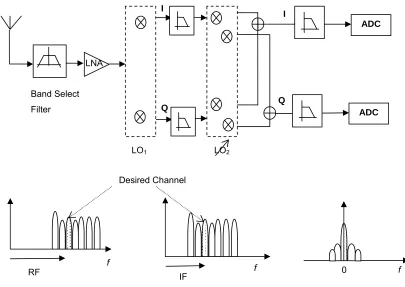
2.8.3 Single Conversion Low-IF Receivers ...32
2.8.4 Double Conversion Wideband-IF Receivers ...33
2.9 CONCLUSION ... 35
CHAPTER 3 THE DUPLEXER ... 36
3.1 INTRODUCTION ... 36
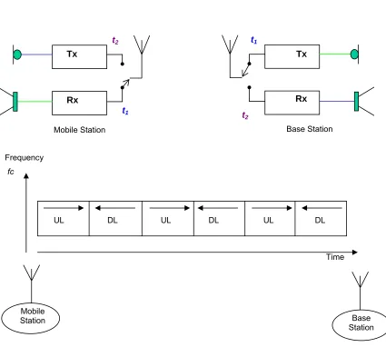
3.2 TDD SYSTEMS ... 37
3.3 FDD SYSTEMS... 38
3.4 INTRODUCTION TO THE DUPLEXER ... 40
3.5 NEED FOR AN ADAPTIVE DUPLEXER IN MULTI-BAND SYSTEMS ... 43
3.6 THE EFFECT OF RECEIVER NON-LINEARITY AND THE Tx LEAKAGE SIGNAL... 45
3.6.1 Receiver Desensitisation ...45
3.6.2 Cross Modulation ...48
3.6.3 Intermodulation Distortion ...51
3.6.3.1 Third Order Intermodulation...52
3.6.3.2 Second Order Intermodulation...54
3.6.4 DC Offset in Direct Conversion Receivers Due to the Tx Leakage Signal ...56
3.7 DUPLEXER REQUIREMENTS... 58
3.8 CONCLUSION ... 61
CHAPTER 4 LITERATURE REVIEW ... 62
4.1 INTRODUCTION ... 62
4.2 TRADITIONAL DUPLEXING FILTERS... 63
4.2.1 Lumped Element Filters...64
4.2.2 Cavity Duplexing Filters ...64
4.2.3 Ceramic Duplexing Filters ...66
4.2.4 SAW Duplexing Filters...68
4.2.5 MEMS Devices ...70
4.2.5.1 MEMS Resonators...71
4.2.6 Stripline or Microstrip Line Duplexing Filters ...74
4.3 REVIEW OF LITERATURE RELATED TO ACTIVE/MULTI-BAND DUPLEXING STRUCTURES ... 77
CHAPTER 5 THE NEW ADAPTIVE DUPLEXER ARCHITECTURE ... 86
5.1 INTRODUCTION ... 86
5.2 THE NEW ADAPTIVE DUPLEXER ARCHITECTURE ... 87
5.3 DESIGN CONSIDERATIONS FOR THE LOW ISOLATION DEVICE ... 91
5.3.1 Wideband Circulator...91
5.3.2 Directional Coupler ...92
5.3.3 Low Selectivity Stripline or Microstrip Filters ...92
5.3.4 Separate Antennas ...93
5.4 CONCLUSION ... 94
CHAPTER 6 DESIGN AND IMPLEMENTATION OF THE SINGLE LOOP CANCELLATION SYSTEM ... 95
6.1 INTRODUCTION ... 95
6.2 SINGLE LOOP CANCELLATION SYSTEM ... 96
6.3 EFFECT OF PHASE AND AMPLITUDE MISMATCH ON SIGNAL CANCELLATION ... 98
6.4 EFFECT OF DELAY MISMATCH ON SIGNAL CANCELLATION ... 102
6.5 SIMULATION OF THE CANCELLATION UNIT WITH SINGLE LOOP ... 105
6.5.1 Signal Cancellation...105
6.5.2 Noise Cancellation ...108
6.6 DESCRIPTION OF THE SINGLE LOOP CANCELLATION SYSTEM... 110
6.7 EXPERIMENTAL RESULTS ... 112
6.8 DOUBLE NULL USING SINGLE LOOP CANCELLATION ... 114
6.9 CONCLUSION ... 117
CHAPTER 7 DESIGN AND IMPLEMENTATION OF THE DOUBLE LOOP CANCELLATION SYSTEM ...119
7.1 INTRODUCTION ... 119
7.2 DOUBLE LOOP CANCELLATION SYSTEM... 120
7.3 DELAY EFFECTS... 123
7.4 THE RELATIONSHIP BETWEEN THE PATH DELAYS AND THE DUPLEXING FREQUENCY ... 124
7.4.1 When 0 <τ1 < τ2...125
7.4.2 When τ1 < 0 and τ2 > 0...128
7.5 DERIVATION OF CONDITIONS FOR |PTX| ≤ 1 AND |QTX| ≤ 1... 130
7.5.1 τ1 > 0 and τ2 > 0...130
7.5.2 τ1 < 0 and τ2 > 0...133
7.6 THE RELATIONSHIP BETWEEN THE BANDWIDTH AND THE ACHIEVABLE CANCELLATION LEVEL ... 136
7.6.1 τ1 Not Equal to τ2...144
7.7 THE PROPOSED ALGORITHM... 147
7.8 EXPERIMENTAL SETUP AND RESULTS... 151
7.9 PERFORMANCE ANALYSIS ... 153
7.10 CONCLUSION ... 157
CHAPTER 8 CONCLUSIONS AND SUGGESTIONS FOR FUTURE WORK...160
8.1 CONCLUSIONS ... 160
8.2 PUBLICATIONS RESULTING FROM THIS WORK ... 162
8.3 SUGGESTIONS FOR FUTURE RESEARCH ... 162
8.3.1 Vector Attenuators ...163
8.3.2 Low Isolation Device...163
8.3.3 Adaptive Control and Algorithm ...163
8.3.4 Integration ...164
8.3.5 Four Loop Cancellation ...164
REFERENCES...168
APPENDIX A - Summary of Standards...186
APPENDIX B - MEMS Based Front End Receiver Architectures ...189
APPENDIX C - Four Cases of Delay Constraints ………...191
APPENDIX D - Delay Effects...192
_______________________________________
List of Figures
Figure 1-1 Conventional duplexer; Hardware structure (left) and frequency
response (right)... 3
Figure 1-2 Adaptive duplexer provides two nulls at the transmitter frequency and the desired receiver frequency... 4
Figure 2-1 Evolution towards third-generation mobile systems in terms of data rate support [18]. ... 20
Figure 2-2 Traditional multi-mode/multi-band receiver... 22
Figure 2-3 An ideal software radio architecture... 23
Figure 2-4 Practical wideband software receiver architecture [20]. ... 25
Figure 2-5 Practical wideband software transmitter architecture [20]... 25
Figure 2-6 Simplified block diagram of a heterodyne receiver architecture. .... 27
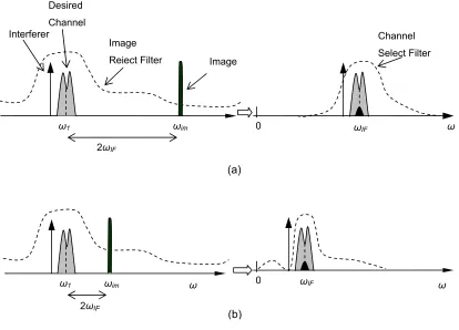
Figure 2-7 Rejection of image vs suppression of interference for (a) high-IF and (b) low-IF [36]. ... 29
Figure 2-8 A simplified block diagram of a homodyne receiver architecture. .. 30
Figure 2-10 A block diagram of a simplified single conversion low-IF receiver
architecture. ... 33
Figure 2-11 Block diagram of a simplified double conversion wideband-IF receiver architecture. ... 34
Figure 3-1 The principle of operation in TDD systems... 37
Figure 3-2 The principle of operation in FDD systems. ... 39
Figure 3-3 Receiver desensitisation... 41
Figure 3-4 Transmitter noise. ... 42
Figure 3-5 The multi-band RF front end (a) using number of duplexers (b) using an adaptive duplexer... 44
Figure 3-6 Receiver blocking. ... 47
Figure 3-7 Cross modulation due to the Tx leakage signal and a jammer signal. ... 49
Figure 3-8 Intermodulation due to LNA non-linearity (two tone test signal). 2ωTx- ωj and 2ωj - ωTx are the third order intermodulation products... 52
Figure 3-9 The effect of third order intermodulation between the Tx leakage signal and a narrowband jammer. ... 52
Figure 3-10 Linear and third order intermodulation products vs amplitude. a3 is normally negative, causing amplifier compression. ... 53
Figure 3-11 Spectrum of the baseband component due to second order distortion caused by the Tx leakage signal in a W-CDMA terminal... 54
Figure 3-12 Effect of second order distortion from the LNA feeding through the mixer... 55
Figure 3-13 Illustration of IIP2. The second order response has a slope of 2. .. 56
Figure 3-14 Self-mixing in DCR due to theTx leakage signal in LO port... 57
Figure 4-2 A six-cavity duplexer and the frequency response [81]... 66
Figure 4-3 A base station duplexer for GSM 1800 [83]. ... 66
Figure 4-4 Dual-mode ceramic puck resonator loaded cavity[86]... 67
Figure 4-5 Construction of a ceramic coaxial resonator [87]. ... 68
Figure 4-6 Structure of a conventional SAW filter (wire bonding type) [91].... 69
Figure 4-7 Schematic diagram of a SAW duplexer [92]. ... 70
Figure 4-8 Film bulk acoustic wave resonator – fabricated on a layer of piezoelectric material placed between top and bottom metal electrodes [104]. ... 72
Figure 4-9 Solidly mounted resonator – fabricated on top of multiple reflectors [97]... 72
Figure 4-10 Photography of the Agilent Technologies produced FBAR duplexer and simplified schematic (designed for CDMA PCS 1900 MHz) [97]. ... 73
Figure 4-11 General microstrip line structure. ... 74
Figure 4-12 General strip line structure. ... 75
Figure 4-13 Schematics of duplexer structures (a) Two SAW filters (one Tx and one Rx) with microstrip line for matching impedance (b) One chip SAW filters (combined Tx and Rx) with stripline for matching impedance [118]. ... 76
Figure 4-14 Simplified diagram of self-cancelling RF communication system (uses the same spectrum at the same time) [121]. ... 78
Figure 4-15 A schematic diagram of the transmitter interference cancellation arrangement for co-located GPS receiver [127]. ... 80
Figure 4-16 Active cancellation concept of the Tx/Rx feedthrough applying an auxiliary transmitter [127]. ... 81
Figure 4-17 A Tx noise cancellation system configuration [128]. ... 82
Figure 4-19 An adaptive duplexer characteristics for dual-path cancellation. Improved duplexing characteristics by achieving double nulls in the receive band of the system... 84
Figure 5-1 The proposed adaptive duplexer architecture... 87
Figure 5-2 Obtaining the error signals from a direct conversion receiver. ... 90
Figure 5-3 (a) A 3-port circulator (b) A circulator used as an isolation device in a transceiver... 91
Figure 6-1 The single loop cancellation configuration. ... 96
Figure 6-2 Vector representation of signal cancellation with phase and gain mismatch... 98
Figure 6-3 The gain phase mismatch with achievable cancellation levels for single loop cancellation...100
Figure 6-4 Achievable cancellation levels with phase mismatch for different values of gain mismatch...101
Figure 6-5 The vector representation of signal cancellation with delay
mismatch...103
Figure 6-6 The delay mismatch with achievable cancellation levels for single loop cancellation...104
Figure 6-7 The schematic diagram of the simulated cancellation unit with single loop. ...106
Figure 6-8 Spectrum of the received signals without the single loop cancellation unit. m1-transmitter interference signal, m2-desired receive signal. ...107
Figure 6-9 Received signal spectrum with the cancellation unit. m1-transmitter interference signal, m2-desired receive signal. ...107
Figure 6-10 The ADS schematic diagram for the noise cancellation. ...109
Figure 6-11 The experimental setup. ...110
Figure 6-13 The 10kHz received signal before the cancellation (a) and after the cancellation (b). Settings: (a)-20mV/square (b)-50mV/square. . 113
Figure 6-14 Error learning curve. ...114
Figure 6-15 Geometric representation of cancellation signals at Tx frequency and Rx frequency using single loop cancellation (a) τ1 ≠ 1/ fd,
(b) τ1 = 1/ fd. ...115
Figure 6-16 Two nulls using single loop cancellation (fd = 190MHz &
fTx = 2GHz). ...116
Figure 7-1 The double loop cancellation configuration. ...120
Figure 7-2 Vector representation of signal components at the double loop summation point (four different delay differences). a) at ωTx
b) at ωRx. For perfect cancellation the vectors must sum to 1.
Note the possible magnitude relationships...122
Figure 7-3 The nulls at Tx and Rx frequencies with double loop cancellation. (a ⇒ τ1 = -1ns τ2 = 0.5ns fd = 190MHz, b ⇒ τ1 = -0.5ns τ2=
0.5ns fd = 190MHz, c ⇒ τ1= -0.5ns τ2 = 0.5ns fd = 45MHz)...124
Figure 7-4 Geometric representation of signal components at the double loop summation point (τ1 > 0 and τ2 > 0). The rotation of Q (P) vector
is caused by a change in frequency of fd acting on the delay path
τ2(τ1). Note here in this cancellation τ2 > τ1because the Q vector
undergoes a greater phase shift. ...125
Figure 7-5 Geometric representation of signal components at the double loop summation point (τ1 < 0 and τ2 > 0). The rotation of Q (P) vector is
caused by a change in frequency of fd acting on the delay path
τ2(τ1). ...128
Figure 7-6 Cancellation signals when |PTx| ≤ 1 and |QTx| ≤1 and the joining
point of the vectors lies in 1st or 2nd quadrant (case (1)). ...130
Figure 7-7 Cancellation signals when |PTx| ≤ 1 and |QTx| ≤ 1 and the joining
point of the vectors lies in the 3rd or 4th quadrant (case (2)). ...132
Figure 7-8 Contours of maximum ( |h1| or |h2| ) for various delay
by fd). The shaded areas show the conditions for coefficient gains
less than unity. ...135
Figure 7-9 Geometrical illustration of the achievable cancellation when the frequency deviates from the null frequencies...137
Figure 7-10 The behaviour of the frequency response. Points E, F, G, H, show the band edges for a cancellation level of |Ca|. ...138
Figure 7-11 Effects of (normalised) delays, τ1fd and τ2fd, on different
(normalised) cancellation bandwidths, B/fd, for a fixed cancellation level of |Ca|2 = -40dB (using Eq. 7-43 ). The curves are
undefined when τ1 = τ2. ...141
Figure 7-12 Bandwidth contours vs τ1 and τ2 when fd = 190MHz and the
cancellation level is <-40dB. The simplified Eq. 7-50 and the original Eq. 7-43 (marked +). Only the first quadrant is shown.
...146
Figure 7-13 Spectrum at LNA input (with the cancellation loop inactivated). ..147
Figure 7-14 Obtaining the cost function from the direct conversion receiver. e1 is the transmitter leakage signal and e2 a pilot used to measure
the noise leakage signal...148
Figure 7-15 The learning curve (τ2 = -τ1, τ1fd = 0.045). ...149
Figure 7-16 Number of iterations for E <-60dB vs τ1 fd
(top: τ2 = 2τ1; bottom τ2 = -τ1). ...150
Figure 7-17 Frequency response of the canceller...151
Figure 7-18 The spectrum of the received signal...152
Figure 7-19 Simulated frequency response of the cancellation unit. (a ⇒ τ1 = -1ns τ2 = 0.2ns fd = 190MHz; b ⇒ τ1 = -τ2 = -1ns;
fd = 190MHz; c ⇒ τ1 = -τ2 = -1ns fd = 45MHz) ...153
Figure 7-20 Experiment results for the cancellation unit. (c ⇒ without the cancellation unit a ⇒ τ1 = -1ns τ2 = 0.2ns
Figure 7-21 Experiment results for the cancellation unit. (c ⇒ without the cancellation unit a ⇒ τ1 = -τ2 = -1ns
fd = 190MHz, b ⇒ τ1 = -τ2 = -1ns fd = 45MHz) ...154
Figure 7-22 Adaptive (b) and Manual (c) frequency response for τ1 = -τ2 = 1.1ns and fd = 45MHz (c) without the cancellation unit. ...156
Figure 7-23 Learning curve of adaptive algorithm for τ1 = -τ2 = 1.1ns and fd = 45MHz...156
Figure 8-1 Four loop cancellation ...165
Figure 8-2 Four loop adaptive duplexer architecture...166
Figure 8-3 Frequency response of the four loop cancellation unit. ...167
Figure B-1 Possible front end receiver architecture utilizing a parallel bank of tuneable/switchable micromechanical filters for a first stage of channel selection [111].. ...189
Figure B-2 MEMS based receiver employing tuneable front end filter - serves partial channel selection and a wide dynamic range for possible fully integrated radio receiver [112]...190
Figure B-3 Proposed MEMS based receiver with acoustic resonant IF filter banks - eliminates the requirement of tuning the first local oscillator, but requires very fast switching speed and low phase-noise at very high oscillator frequencies [112]...190
Figure D-1 Magnitude of h1 for various delay differences in path1 and path2.. ...192
Figure D-2 Magnitude of h2 for various delay differences in path1 and path2.. ...192
Figure E-1 Photographs of the single loop cancellation system. ...193
Figure E-2 Photographs of the double loop cancellation system. ...194
_______________________________________
List of Tables
Table 2-1 Major analogue cellular system standards [2]... 12
Table 2-2 Second generation digital cellular standards summary [3], [4] ... 13
Table 2-3 W-CDMA (UMTS) technical summary [13]... 19
Table 2-4 CDMA2000 technical summary [14] ... 20
Table 3-1 Anticipated performance for W-CDMA duplex arrangement [56]... 43
Table 3-2 Summary of RF receiver requirements for 3G W-CDMA mobile equipments [56]. ... 57
Table 3-3 Duplexing frequency and frequency bandwidth ... 58
Table 3-4 The maximum output power ... 59
Table 3-5 The receiver sensitivity level... 60
Table 6-1 Noise voltages at different nodes...109
Table 7-1 n1 and n2 for different cases ...139
Table 7-2 l1, l2 and l3 for different cases...140
Table A-1 PCS standards overview [3] ...186
Table A-2 Digital cordless air interface parameters summary [3] ...186
Table A-3 TD-CDMA technical summary [15]...187
Table A-4 TD-SCDMA technical summary [16] ...188
_______________________________________
List of Abbreviations
1G, 2G, 2.5 And 3G 1st 2nd Intermediate and 3rd Generation Systems 3GPP Third Generation Partnership Project
ADC Analogue to Digital Conversion ADS Advanced Design System
AIN Aluminium Nitride
AM Amplitude Modulation
AMPS Advanced Mobile Phone Service AMR Adaptive Multi-Rate
ARIB Association of Radio Industries and Business ASIC Application Specific Integrated Circuit BAW Bulk Acoustic Wave
Bi-CMOS Bi-Polar Complementary Metal-Oxide Semiconductor
BPF Band-pass Filters
BS Base Station
CAD Computer Aided Design CDMA Code Division Multiple Access
CMOS Complementary Metal-Oxide Semiconductor CRC Cyclic Redundancy Check
CW Continuos Wave
DAC Digital to Analogue Converter
D-AMPS Digital-Advanced Mobile Phone Services
DC Direct Current
DCR Direct Conversion Receiver
DCS 1800 Digital Communication System 1800
DQPSK Differential Quadrature Phase Shift Keying
DR Dynamic Range
DS-CDMA Direct Sequence-Code Division Multiple Access DSP Digital Signal Processing
EDGE Enhanced Data Rates for Global Evolution EFR Enhanced Full Rate
ETACS Extended Total Access Communication System ETSI European Telecommunications Standards Institute EV-DO Evolution-Data Optimized
EV-DV Evolution-Data and Video
FBAR Film Bulk Acoustic Wave Resonator FDD Frequency Division Duplex
FDMA Frequency Division Multiple Access FFSK Fast Frequency Shift Keying
FIR Finite Impulse Response FM Frequency Modulation
FPGA Field Programmable Gate Arrays
FPLMTS Future Public Land Mobile Telecommunication Systems GaAs Gallium Arsenide
GFLOPS Giga Floating Point Operations per Second GMSK Gaussian Minimum Shift Keying
GPRS General Purpose Radio Services GPS Global Positioning System
GSM Global System of Mobile Communication HEM Dual Hybrid Electromagnetic Modes HPA High-Pass Amplifier
HS High Speed
HSCSD High Speed Circuit Switched Data HSPDA High Speed Packet Downlink Access HTS High-Temperature Superconductor
IF Intermediate Frequency
IMD Intermodulation Distortion
IMT-2000 International Mobile Telecommunications for the Year 2000 IMT-DS IMT-Direct Sequence
IMT-FT IMT-Frequency Time IMT-MC IMT-Multi Carrier IMT-SC IMT-Single Carrier IMT-TC IMT-Time Code
IP2 Second Order Intercept Point IP3 Third Order Intercept Point
IS-54, IS-95, IS-136 Interim Standard 54, 95, 136 ITU International Telecommunication Union JDC Japan Digital Cellular
LMS Least-Mean Square
LNA Low Noise Amplifier
LO Local Oscillator LPF Low-Pass Filter
LTCC Low-Temperature Co-Fired Ceramic MEMS Micro Electro-Mechanical Systems MIMO Multiple Input Multiple Output
MMIC Monolithic Microwave Integrated Circuit
MS Mobile Station
MSPS Million Sampling Per Second
NF Noise Figure
NMT Nordic Mobile Telephone
NTT DoCoMo Nippon Telegraph and Telephone Do Communications over the Mobile Network Also DoCoMo Means "Anywhere" In Japanese
OFDM Orthogonal Frequency Division Multiplexing OHG Operators Harmonization Group
OIP3 The Third order Output Intercept Point PDC Pacific Digital Cellular
PHS Personal Handy Phone Systems
PN Pseudonoise
PSD Power Spectrum Density
PZT Lead Zirconate Titanate QCELP Qualcomm Purevoice
QPSK Quadrature Phase-Shift Keying
RELP-LTP Regular Pulse Excited Linear Prediction-Long Term Prediction RF Radio Frequency
RLS Recursive Least-Squares
RTT Radio Transmission Technologies SAW Surface Acoustic Wave
SID Sound Interface Device SiGe Silicon Germanium
SISO Single Input Single Output SMR Solidly Mounted Resonator SNR Signal to Noise Ratio
SVD Singular Value Decomposition TACS Total Access Communication System TD-CDMA Time Division CDMA
TDD Time Division Duplex
TDMA Time Division Multiple Access TD-SCDMA Time Division Synchronous CDMA TE Transverse Electric Modes
TIA Telecommunications Industry Association
TM Transverse Magnetic Modes
TTA Telecommunications Technology Association
UL Up Link
UMTS Universal Mobile Telecommunications Systems UTRA UMTS Terrestrial Radio Access
UWC Universal Wireless Communication VLSI Very Large-Scale Integration
VSELP Vector Sum Excited Linear Prediction
WARC-92 World Administrative Radio Conference In 1992 W-CDMA Wideband Code Division Multiple Access W-LAN Wireless Local Area Network.
WRC-2000 World Radio Conference In 2000
_______________________________________
List of Symbols
ai ith order non-linearity constant Aj amplitude of the jammer signal
ARx amplitude of the desired receive signal
ATx amplitude of the transmitter interference signal
B bandwidth of the cancellation signal
C cancellation signal c correction factor
E cost function of the algorithm e1 error signal 1
e2 error signal 2
f frequency
fδ frequency deviation with respect to fTx or fRx
fδ frequency of the Tx pilot signal fc carrier frequency
fd duplexing frequency
fj jamming signal
fLO frequency of the local oscillator
Fr receiver noise figure
fRx receivefrequency
Ft transmitter noise figure
fTx transmit frequency
h1 complex gain/attenuation of the cancellation path1
h2 complex gain/attenuation of the cancellation path2
k Boltzmans constant m modulation index NRx receiver noise floor
Out desired signal
OutRx desired signal at Rx frequency
OutTx desired signal at Tx frequency
P’Tx the Tx leakage power at the input of the receiver
Pcmod cross modulation power referred to input of the receiver
Pip the receiver third order input intercept point power
Pjam the single tone jammer signal at the input of the receiver
PRx signal vectors of cancellation path1 at Rx frequency
PTx signal vectors of cancellation path1 at Tx frequency
Pu the power of the undesired signal
Px signal vector of cancellation path1
QRx signal vectors of cancellation path2 at Rx frequency QTx signal vectors of cancellation path2 at Tx frequency Qx signal vector of cancellation path2
R V22/ V12 in dB
SRx desired receive signal
Sx transmitter interference signals
T room temperature
Ts span of the delay variation
V1 gain of the reference (interference) signal
V2 gain of the resultant signal
x(t) input to the system
y cancellation signal
%d the percentage of modulation on the desired signal due to cross modulation
θ relative phase error of the cancellation signal
φj phase of the jammer signal
φRx phase of the desired receive signal
φTx phase of the transmitter interference signal ωd angular duplexing frequency
ωIF angular frequency of the intermediate frequency signal
ωj angular frequency of the jammer signal
ωLO angular frequency of the local oscillator
ωm angular frequency of the modulated signal
ωRF angular frequency of the RF signal
ωRx angular frequency of the desired receive signal
ωTx angular frequency of the transmitter interference signal
δ relative gain error of the cancellation signal δfd mismatch of duplexing frequency
β relative phase of the resultant signal
βRx phase difference between the leakage and the cancelling path at
Rx frequency
βTx phase difference between the leakage and the cancelling path at
Tx frequency
α the amount of cross modulation power that penetrates into the in-band signal (the soaking factor)
τ1 the delay difference between the main path and the cancellation path1 (τb-τa)
τ2 the delay difference between the main path and the cancellation path2 (τc-τa)
τa main path delay
τb cancellation path1 delay
τc cancellation path2 delay
∆V1 (1+δ) in dB
|C|2 residual signal power
________________________________________________________
CHAPTER 1
Introduction
1.1
The Introduction to the Thesis
next years future fourth generation mobile systems will be added to this list. All schemes are capable of full duplex operation. No single standard covers all areas and all service requirements, so users will require multi-mode/multi-band handsets. To do this in a very small package is a difficult task.
The software radio approach is to replace many of the traditional analogue radio functions, such as channel selection, demodulation and synchronization, with digital signal processing (DSP). Configuring the radio to different standards becomes a software exercise. The remaining radio functions must be made generic (multi-band), the analogue to digital interface must have large dynamic range and the DSP sections must have low power consumption. It is interesting to note that over the past years tremendous progress has been made in reducing the part count of the baseband functions of a wireless mobile. However, little progress has happened in the RF functions. Today third generation mobile communication systems (3G) are at the beginning of their introduction. Through a number of technological advancements the evolution of practical software radio is accelerating. Some of these technologies making significant contributions include wideband RF devices, smart antennas, and integrated circuits.
Figure 1-1 Conventional duplexer; Hardware structure (left) and frequency response (right).
A duplexer can be built in many ways using classical resonant circuits (e.g. ceramic or cavity resonators). Recently, duplexers are being built using multilayer technology with the use of slotline or microstrip line coupling structures to improve the level of integration. Other popular techniques include Surface Acoustic Wave(SAW) and Film Bulk Acoustic Wave Resonator (FBAR) devices.
Existing duplexers cannot be implemented in an integrated circuit. Here in this thesis an adaptive/active duplexer architecture that eliminates the need for multiple duplexers or reduces their requirements for software radio implementation is proposed. The adaptive duplexer architecture involves a reduced isolation circuit or device combined with a double loop cancellation process. Using this technique it is possible to obtain two adjustable nulls for cancelling the transmitter leakage signal (at frequency fTx) and its associated noise components (at frequency fRx) that fall in the receiver band (Figure 1-2).
fRx
Tx Rx
BPFTx BPFRx fTx fRx
Rx Band
Tx Band
Duplexing Offset
f
BPFTx BPFRx
Figure 1-2 Adaptive duplexer provides two nulls at the transmitter frequency and the desired receiver frequency.
1.2
The Objective of the Thesis
The aim of this project is to study the feasibility of replacing or partially replacing the duplexing filter with an active cancellation unit. The unit will bleed a controlled amount of out-of-phase signal into the receiver front end to subtract out the jamming signal.
1.3
Contribution to Knowledge
The pace of change in telecommunications technology is increasing rapidly. In the area of mobile telephone systems, researchers are already exploring new technologies to realize a software radio system that supports multiple mobile telephony standards and multi-mode operation. The adaptive duplexer architecture in this work removes a significant barrier in the successful implementation of the software radio concept thus allowing the users of the mobile telephones to use a single handset to subscribe to all services. A duplexer that can handle multiple bands and which will enable a “future proof” solution by allowing the addition of new bands with different duplexing separations is at present unavailable. Hence,
Tx Leakage Signal
Rx Signal
Rx Noise Tx Noise
Two Nulls
fTx fRx f
Power
Adaptive Duplexer Frequency
this work on an adaptive duplexer with these capabilities will be a significant contribution to the realization of the software radio concept.
1.4
Summary of Findings
• A novel adaptive duplexer architecture that eliminates the need for multiple duplexers in a software radio front end is presented. Using this method the required transmitter leakage isolation and required transmitter noise cancellation levels that meet the 2G and 3G mobile wireless standards were achieved. A Tx leakage cancellation level of 66.8dB and a Tx noise cancellation of 58dB were achieved over a 5MHz bandwidth using a 190MHz duplexing frequency. This satisfies the typical requirement for a WCDMA duplexer of 48dB to 60dB.
• Cancellation performance is shown to be affected by delay differences between the main path and the cancellation paths. The tolerable delay variation depends on the dynamic range of the control elements in the cancellation paths. The achievable cancellation also depends on the duplexing frequency and systems with smaller duplexing frequencies achieve higher cancellation levels.
• The behaviour of the double loop cancellation technique is identified for the first time using geometrical analysis. This leads to an in depth knowledge of double loop cancellation theory that helps in determining important design parameters.
• It is shown that the delay difference close to zero in either of the cancellation paths results in a wide bandwidth. The coefficient values of the cancellation paths become very large when the difference of the path delays is close to an integral number of the reciprocal of the duplexing frequency and this condition must be avoided.
• An expression for the achievable cancellation level at a specified bandwidth is derived in terms of the delays and the duplexing frequency. It is shown that the relationship between the cancellation bandwidth and the achievable cancellation level is linear (6dB/octave). It is also shown that the residual signal power (|C|2) is proportional to the bandwidth (B) squared, duplexing frequency (fd) squared and the time delays (τ1, τ2)
squared ( 2 π4 2
( ) ( ) ( )
2 τ1 2 τ2 2d
f B
C = ).
• Cancellation in the Tx band and cancellation in the Rx band are shown to be interdependent. Therefore the control algorithm must use a cost function, which when minimised, provides cancellation in both bands. A new algorithm to achieve the required dual band cancellation is described.
1.5
Publication Summary
The following publications have resulted in from this research.
Conference Papers
1. S. Kannangara and M. Faulkner, “Adaptive Duplexer for Software Radio,”
2 nd ATcrc Telecommunications and Networking Conference, Fremantle,
WA, Australia, 16-18 October 2002.
2. S. Kannangara and M. Faulkner, “Simulation of a Cancellation Unit in an Adaptive Duplexer for Software Radio,” Proceedings of the 4th International Conference on Modelling & Simulation MS’02, Melbourne Australia, 11-13 November 2002, pp. 148-152.
3. S. Kannangara and M. Faulkner, “Adaptive Duplexer for Multiband Transreceiver,” IEEE Proceedings of Radio and Wireless Conference,
4. S. Kannangara and M. Faulkner, “Effects of Delay Differences in Double Loop Cancellation on Active Wideband Duplexer,” 7th International
Symposium on Digital Signal Processing and Communication Systems,
Gold Coast, Australia, 8-11 December 2003.
5. S. Kannangara, M. Williamson and M. Faulkner, “Performance Analysis of the Cancellation Unit in an Adaptive Wideband Duplexer for Software Radio,” 3rd ATcrc Telecommunications and Networking Conference,
Melbourne, Australia, 11-12 December 2003.
6. M. Williamson, S. Kannangara, and M. Faulkner, “Performance Analysis of Adaptive Wideband Duplexer,” Australian Telecommunications
Networks and Applications Conference, Melbourne, Australia, 8-10
December 2003.
Journal Articles
7. S. Kannangara and M. Faulkner, “Simulation of a Cancellation Unit in an Adaptive Duplexer for Software Radio,” AMSE Best of book 2002, AMSE press, pp.63-72, 2003.
8. S. Kannangara, and M. Faulkner, “An Algorithm to Use in Adaptive Wideband Software Radio”, IEICE Transactions on Communications, vol. E86-B, no. 12, pp. 3452-3455, December 2003.
1.6
Organisation of the Thesis
This thesis is organized in eight chapters. Chapter 1, which corresponds to this introduction, states the objective, provides a contribution to knowledge, summary of findings, publications summary and a thesis overview.
Chapter 2 reviews the technology background. First it summarises the 1st and2nd generations of mobile cellular systems. Next the 2.5 generation, that extends the 2nd generation platform to provide data rate enhancements and other premium services, is briefly looked at. Then the 3rd generation systems that bring about revolutionary changes are discussed. The convergence of different mobile cellular standards to form a unified 3G standard is also discussed along with a brief introduction to future 4th generation systems. The software radio as a concept to implement multi-band/multi-mode systems is also investigated. The duplexer front end component is recognised as one of the main challenges in realisation of a practical software radio. Finally some receiver architectures which are particularly suitable for integration and multi-band systems are examined.
Chapter 3 gives an introduction to the duplexer. Here the need for an adaptive duplexer for software radio is investigated. When a high transmitter leakage signal is present at the receiver input, a number of non-linear adverse effects can occur that degrade the receiver sensitivity. These include desensitisation, blocking, cross modulation and intermodulation and are discussed in this chapter. The main requirements associated with a duplexer are also specified.
A review of existing duplexing filter technologies along with a review of the literature associated with active duplexing structures are discussed in Chapter 4.
Chapter 6 concentrates on the single loop cancellation method. This part of the research focussed only on the cancellation of the Tx leakage signal at the receiver. The work includes design and implementation details and also investigates phase and gain mismatches, delay effects and the control algorithm. Finally the experimental results are presented.
The new double loop cancellation system that suppresses both the Tx leakage and the Tx noise signals is presented in Chapter 7. The system is analysed using a geometric method. The influence of various parameters on the cancellation is examined. A new algorithm that controls the cancellation process is offered and the experimental results are presented.
________________________________________________________
CHAPTER 2
Technology Background
2.1
Introduction
Second generation mobile communication systems were created to address the need for increased capacity over first generation analogue systems. It is expected that at the beginning of 3G operation the second generation systems would coexist. Therefore transceivers should support both 2G and 3G functional requirements. Since the user preference is for a single mobile terminal, the transceiver requires multi-mode/multi-band capabilities. The software radio concept is being developed as a solution to this problem. There are many issues still to be addressed in the realisation of the software radio concept. The duplexer is one of the main problems of the RF front end since it is a fixed frequency component.
perspective are discussed in the next section. The adaptive duplexer in this research is based on a direct conversion receiver architecture (DCR) which is more suitable for software radio design. The direct conversion receiver is examined with some other receiver architectures in the final section.
2.2
1
stGeneration Systems
With the invention of microprocessors and the cellular communications concept in the 1970s and 1980s, the first generation (1G) mobile communication systems were born [1]. First generation systems use cellular coverage, where the coverage area is divided into small cell areas. The 1G systems were essentially analogue systems using Frequency Division Multiple Access (FDMA) to communicate and were designed for voice transmission only (no data). NMT (Nordic Mobile Telephone), AMPS (Advanced Mobile Phone Service), TACS (Total Access Communication System), ETACS (Extended Total Access Communication System), JDC (Japan Digital Cellular) etc., were among first generation systems. NMT was the first analogue cellular phone system that started operating in Scandinavia in 1979. In the beginning, it used the 450MHz band and therefore was named NMT 450. Later it used the 900MHz band because of the need for more capacity and was called NMT 900. AMPS was introduced in 1978 by the Bell telephone company in the USA and started operation in 1983 in Chicago. TACS was introduced in UK in 1982. ETACS was the extended version of TACS and was deployed in 1985. The cellular systems called C-450 (operated in the 450 MHz band) and Radicom 2000 (operated in the 200 MHz band) were also introduced in Germany and in France respectively in 1985.
Table 2-1 Major analogue cellular system standards [2]
Specification AMPS TACS NMT450 NMT900
Channels 832 1320 180 1000/2000
TX frequency 824-849 872-905 453-457.5 (& other bands) 872-905
Channel
separation 30kHz 25kHz 25/30kHz 25kHz/12.5
Frequency stability ± 2.5 PPM ± 2.5 PPM ± 5. PPM ± 5 PPM
Tx power 3 watts 2.8 watts 1 5 watts 3 watts
Voice deviation 12kHz 9.5kHz 4.7kHz 4.7kHz
Data deviation 8kHz 6.4kHz 3.5kHz 3.5kHz
Receiver
sensitivity 12dBc @-116dBm 20dBc @-113dBm
20dBc
@-113dBm 20dBc @-113dBm
Adjacent channel
selectivity 60dB 55dB 70dB 70dB
Spurious rejection 60dB 65/55dB 70dB 70dB
Intermodulation 65dB 65/55dB 67dB 67dB
Signalling method Manchester Manchester FFSK FFSK
Speed 10kbps 8 kbps 1.2kbps 1.2 kbps
Duplexing method FDD FDD FDD FDD
2.3
2
ndGeneration Systems
generation cellular systems. The four most popular 2G cellular radio standards [3], [4] are listed in Table 2-2.
Table 2-2 Second generation digital cellular standards summary [3], [4]
Specification GSM IS-54 PDC IS-95
Year of
introduction 1990 1991 1993 1993
Frequencies 890-915 MHZ(R) 935-960 MHz (F)
824-849 MHz (R) 869-894 MHz (F)
810-830 & 1429-1453 MHz (R) 940-960 & 1477-1501 MHz (F)
829-849 & 1850-1910 MHz (R) 940-960 & 1477-1501MHz (F)
Multiple access TDMA/FDMA/FDD TDMA/FDMA/ FDD TDMA/FDMA/ FDD CDMA
Modulation GMSK (BT=0.3) π/4 DQPSK π/4 DQPSK QPSK OQPSK
Carrier
separation 200kHz 30kHz 25kHz 1.25MHz
Channel data
rate 1 270.833kbps 48.6kbps 42kbps 19.2kbps
Number of voice
channels 1000 2500 3000 4000
Spectrum efficiency (overall bit rate)
1.35bps/Hz 1.62bps/Hz 1.68bps/Hz 2.58bps/Hz
Speech coding RELP-LTP @ 13kbps VSELP @7.95kbps VSELP @ 6.7kbps QCELP @ 9.6kbps / @ 14.4kbps
Channel coding CRC with R=1/2; L=5 Conv. 7 bit CRC with r=112;
=6 Conv. CRC with Cony. NA
Equalizers Adaptive Adaptive Adaptive Adaptive
Portable Tx.
power max./ avg. 1 W/125mW
600mW/200
mW 125mW 200mW
Duplexing
method TDD/FDD TDD/FDD TDD/FDD FDD
countries to replace old analogue networks. Currently the maximum data rate for GSM is 14.4kbps. IS-95 is based on narrowband spread spectrum technology and uses 1.25MHz channel bandwidth. Therefore it offers increased capacity, wider bandwidth and is very flexible because it uses CDMA access method. IS-95 and IS-136 are capable of operating in the same band as AMPS and specified to be dual-mode systems. 2G systems compared with 1G systems allow more efficient use of the radio spectrum since they can handle more calls than analogue FDMA technology.
PDC is the Japanese 2G standard. It is somewhat similar to IS-54 standard, but uses 4-ary modulation for voice and control channels, making it more like IS-136 in North America [3].
DCS 1800 (Digital Communication System 1800) and PHS are also included in 2G PCSs [3] and are listed in Table A-1 in Appendix A. The major 2G digital cordless air interface standards [3] are also listed in Table A-2 in Appendix A.
2.4
2.5 Generation Systems
2.5 generation systems address the data capacity limitations associated with the 2nd generation systems. Even though the boundary between 2G systems and 2.5G systems is somewhat unclear, 2.5G systems provide clear upgrades to the 2G systems that almost make it possible to provide similar capabilities as 3G systems. A number of technologies are commonly used to provide these capabilities such as High Speed Circuit Switched Data (HSCSD), Enhanced Data rates for Global Evolution (EDGE) and General Purpose Radio Services (GPRS).
way to upgrade the current wireless platform as the changes involve only upgrading the software used in the network.
Using GPRS, data rates up to 115kbps with error correction are possible using approximately eight time slots. This technology is based on packet switching and thus makes efficient use of the available bandwidth using variable bit rates. It is also suitable for services that use bursty data due to its ability to dynamically allocate resources.
EDGE is an improvement over GSM which increases the traditional GSM data rates over 300%. It uses eight phase shift keying (8 PSK) method for modulation. This is an attractive solution for existing GSM networks as the change required is only a software upgrade. Due to its ability to co-exist with the Gaussian minimum shift keying modulation, it allows users to continue using their current handsets. IS-136 also can be upgraded using EDGE.
In addition to these methods, NTT DoCoMo (Nippon Telegraph and Telephone DoCoMo) from Japan has developed their own proprietary packet based technology called i-mode which provides users an efficient mechanism for wireless internet browsing and email access.
2.5
3
rdGeneration Systems
The key objectives of 3G development are to provide [6]:
• multi-standard user terminals that operate effectively for all types of services, in all radio environments
• service quality that is comparable to the current fixed public network
• flexible new capabilities and services such as WWW, high bit-rate data and multimedia
• network to air interface flexibility
• compatibility with second generation e.g. GSM/DCS
• “Future proof” systems to easily accommodate added capabilities
The main requirements that apply to third generation systems are [7]:
• support for high data rates up to at least 144kbits/s (384kbits/s for full area coverage) in all radio environments and up to 2Mbits/s in low mobility and indoor environments
• support for symmetrical and asymmetrical data transmission
• support for packet-switched and circuit switched services, such as Internet (IP) traffic and real-time video
• support for good voice quality (compatible with wireline quality)
• support for greater capacity and improved spectrum efficiency compared with existing second-generation wireless systems
• support for several simultaneous services to end-users and terminals – that is, for multimedia service capabilities
• support for coexistence and interconnection with mobile satellite services
• support for roaming, including international roaming, between different IMT-2000 (International Mobile Telecommunications for the year 2000) operators
• support for scale-of economy and an open global standard to meet mass-market needs
studies on global personal telecommunications in 1986. The ITU World Administrative Radio Conference in 1992 (WARC-92) identified 230MHz, in the 2GHz band, on a world wide basis for the satellite and terrestrial components of Future Public Land Mobile Telecommunication Systems (FPLMTS) [8]. Later it was renamed as IMT-2000. WRC-2000 (World Radio Conference in 2000) identified three additional bands i.e. 806-960MHz, 1710-1885MHz and 2500-2690MHz for terrestrial IMT-2000.
The European Telecommunications Standards Institute (ETSI) regards 3G systems as UMTS. In 1998 the first decision in the standardisation process of UMTS was made by ETSI. ETSI chose the W-CDMA concept to be adopted in the spectrum (for uplink one band of spectrum and for down link another band of spectrum, - FDD duplex mode) of UMTS. It also chose the TD-CDMA (Time Division-CDMA) concept to be adopted in unpaired band (a single monolithic block of spectrum – TDD duplex mode) of UMTS. UMTS will consist of both satellite and terrestrial components as in IMT-2000 and will support both circuit-switched and packet-circuit-switched services. The Telecommunications Technology Association (TTA) in South Korea and Association of Radio Industries and Business (ARIB) in Japan have developed standards based on W-CDMA. The Telecommunications Industry Association (TIA) in United States proposed CDMA2000. The major difference between W-CDMA and CDMA2000 is that W-CDMA is backward compatible with GSM networks and CDMA2000 is backward compatible with IS-95 networks [9]. Due to the different technologies used in different regions in the world, a family of compatible standards were adopted under IMT-2000 umbrella.
The five standards included in IMT-2000 terrestrial radio interfaces are shown below [10], [11].
at a chip rate of 3.84Mcps, spread over approximately 5MHz. This mode of operation will be used in the UMTS macro and micro-cellular environment. 2. IMT-MC (Multi-Carrier CDMA - FDD duplex type) - This is known as
CDMA2000. This has been specified by 3GPP2 and operates on the downlink at a basic chip rate of 1.288Mcps, occupying 1.25MHz of bandwidth.
3. IMT-TC (Time Code CDMA - TDD duplex type) - This is known as TD-CDMA. It is a combination of the UTRA TD D and the TD-STD-CDMA. This operates in unpaired spectral bands at a chip rate of 3.84Mcps, spread over approximately 5MHz.
4. IMT-SC (Single Carrier - FDD duplex type) - This is known as UWC-136 and proposed by the Universal Wireless Communication (UWC) Consortium and Telecommunication Industry Association (TIA). It represents convergence between the TDMA-136, GSM and EDGE standards. UWC-136 will adopt the GPRS packet data network architecture, while enhancing the TDMA-136 radio interface to include GSM/EDGE compatibility and a high data rate indoor solution. The UWC-136 solution provides backward compatibility with the AMPS, 54, IS-136 and GSM networks.
5. IMT-FT (Frequency Time - TDD duplex type) - This is known as DECT.
In May 1999, the Operators Harmonization Group (OHG) concluded the harmonization discussion at a meeting in Toronto, Canada, which resulted in a single 3G CDMA standard with three modes; i.e. a direct sequence mode based on W-CDMA, a multi-carrier mode based on CDMA2000 and a TDD mode based on UTRA TDD [12]. Combined time division and code division multiple access scheme is used in UTRA TDD.
Table 2-3 W-CDMA (UMTS) technical summary [13]
Frequency band 1920MHz -1980MHz and 2110MHz - 2170MHz (Frequency Division Duplex) UL and DL
Minimum frequency band
required ~ 2x5MHz
Frequency re-use 1
Carrier spacing 4.4MHz - 5.2MHz
Maximum number of (voice)
channels on 2x5MHz ~196 (spreading factor 256 UL, AMR 7.95kbps) / ~98 (spreading factor 128 UL, AMR 12.2kbps)
Voice coding AMR codecs (4.75kHz - 12.2kHz, GSM EFR=12.2kHz) and SID (1.8kHz)
Channel coding Convolutional coding, Turbo code for high rate data Duplexer needed (190kHz separation), Asymmetric connection supported
Tx/Rx isolation MS: 55dB, BS: 80dB
Receiver Rake
Receiver sensitivity Node B: -121dBm, Mobile -117dBm at BER of 10-3
Data type Packet and circuit switch
Modulation QPSK
Pulse shaping Root raised cosine, roll-off = 0.22
Chip rate 3.84Mcps
Channel raster 200kHz
Maximum user data rate (physical
channel) ~ 2.3Mbps (spreading factor 4, parallel codes (3 DL / 6 UL), 1/2 rate coding), but interference limited.
Maximum user data rate (offered) 384 kbps (year 2002), higher rates ( ~ 2 Mbps) in the near future. HSPDA will offer data speeds up to 8-10 Mbps (and 20 Mbps for MIMO systems)
Channel bit rate 5.76Mbps
Frame length 10ms (38400 chips)
Number of slots / frame 15
Number of chips / slot 2560 chips
Power control period Time slot = 1500Hz rate
Power control step size 0.5, 1, 1.5 and 2dB (Variable)
Power control range UL 80dB, DL 30dB
Mobile peak power Power class 1: +33 dBm (+1dB/-3dB) = 2W; class 2 +27 dBm, class 3 +24 dBm, class 4 +21 dBm
Number of unique base station
Table 2-4 CDMA2000 technical summary [14]
Frequency band Any existing band. (Frequency Division Duplexing)
Minimum frequency band required 1x: 2x1.25MHz, 3x: 2x3.75
Chip rate 1x: 1.2288, 3x: 3.6864Mcps
Maximum user data rate 1x: 144 kbps now, 307kbps in the future 1xEV-DO: max 384 kbps - 2.4 Mbps, 1xEV-DV: 4.8Mbps.
Frame length 5ms, 10ms or 20ms
Power control rate 800Hz
Spreading factors 4 ... 256 UL
The evolution of the third-generation mobile telecommunication system IMT-2000, in terms of data rate support [18] is shown in Figure 2-1. The capability targets for the 3G have been defined as 384 kbit/s for full area coverage and 2Mbit/s for local area coverage.
Figure 2-1 Evolution towards third generation mobile systems in terms of data rate support [18].
W-CDMA is capable of providing more capacity as it uses a 4 times wider channel allocation compared to narrow band CDMA. It is based on the radio
2.5 G
3 G 2 G
9.6kbit/s
TDMA/FDMA PDC
9.6 (14.4)kbit/s TDMA/FDMA
GSM
19.2kbit/s
TDMA IS-136 (D-AMPS)
8.0 (13.0)kbit/s CDMA IS-95 (cdmaOne)
45-160 kkbit/s GPRS
384kbit/s EDGE
56kbit/s HSCSD
64kbit/s IS-95 B
43.2kbit/s IS-136+
IMT-2000 144-384 kbit/s, 2Mbit/s
TDMA UWC-136
n*64 kbit/s, 2Mbit/s CDMA CDMA2000
144-384kbit/s, 2Mbit/s W-CDMA/TD-CDMA
UMTS
access technique proposed by the ETSI Alpha group and the specifications were finalised in 1999 [13].
The AMPS, GSM, IS-95 (CDMA) and UMTS FDD (W-CDMA) standards are of particular interest to this thesis as they all specify FDD operation and therefore require a duplexing filter.
2.6
4
thGeneration Systems
As envisaged currently, the 4th generation systems will involve providing IP connectivity over the wireless interface. It will encompass all 2nd and 3rd generation wireless mobile technologies and will provide a standard that ensures the interoperability between satellite and terrestrial wireless mobile technologies and W-LANs (Wireless Local Area Networks). Interoperability of network technologies is going to be a major challenge in 4G systems. It is projected that the 4G systems will provide at least 100 Mbps peak data rates in full-mobility wide area coverage and 1 Gbps in low-mobility local area coverage [19]. OFDM (Orthogonal Frequency Division Multiplexing) modulation, multiple antenna technology and CDMA are being considered as elements for 4G systems.
2.7
The Software Radio
digitised. In software radio the emphasis is given to replace most of the traditional RF functions by digital signal processing techniques. So that the user can have one single transceiver that can tune to different channels of different wireless systems. Software radio will allow the terminals to connect to multiple networks that use different air interface standards. Switching between different wireless standards becomes only a software upgrade without a need to change or upgrade hardware. An excellent overview and discussion on the software radio concept/architecture is presented in [22], [23].
A simple realization concept of a multi-mode receiver that consists of switched multiple traditional receiver chains is shown in Figure 2-2. The required channel is selected by using a fixed channel select filter at an intermediate frequency and channel bandwidth set by the parameters of the particular standard.
Figure 2-2 Traditional multi-mode/multi-band receiver.
The ideal software radio architecture is shown in Figure 2-3. In this concept the analogue to digital conversion is carried out directly at the front end. Here, the entire band under consideration, which consists of number of channels, will be digitised so that all functions of the radio can be performed using programmable Digital Signal Processing (DSP) microprocessors or Field Programmable Gate Arrays (FPGAs) or some dedicated Application Specific Integrated Circuits
CH1
CH2
CH3
CHn
Analogue Channel Selection
f
Analogue
Functions A/D Digital Functions
Analogue
Functions A/D Digital Functions
Analogue
Functions A/D Digital Functions
Analogue
Functions A/D Digital Functions
. . .
. . .
. . .
GSM 900
DCS 1800
UTRA-FDD
(ASICs). Hence the ideal receiver architecture can be reconfigured to suit any RF band, modulation or data format. This makes it capable of operating within any communications network and would have significant benefits such as reduction of size, cost and power consumption of radio systems.
Figure 2-3 An ideal software radio architecture.
If the radio functions are performed using DSP, the new features and upgrades could be done using software upgrades, which become only a reprogramming task. The other significant advantage of using software radio is its ability to support multiple standards. With software radio the receiver could be programmed to receive incompatible technologies such as TDMA (Time Division Multiple Access), GSM and CDMA in the same receiver.
However there are a number of challenges that lie ahead in achieving this concept, mainly in the speed of current Analogue to Digital Conversion (ADC) and DSP capabilities. The total digital processing requirements in such a radio may add up to more than 10GFLOPS (Giga Floating Point Operations per Second) [22]. By January 2005 Texas Instruments have accelerated their fastest DSP to 1500MFLOPS (Mega Floating Point Operations per Second) [24]. Still this is not sufficient for processing the entire radio functionality required by software radio. Since the band of interest could be many megahertz wide (3G mobile’s spectrum is 200MHz) and is in the microwave frequency range, it requires very high speed
ADC
ADC
DSP Ideal
Isolator/Circulator/ Coupling Device Digital
Channel Selection
CH1
CH2
.
. . . . . .
CHn
ADCs to sample the signal. The ADCs must satisfy the Nyquist criterion for sampling so that the original signal can be digitised without the risk of losing information. Up to 500MSPS (Million Sampling per second) of sample rate will be required by 3G mobile with 200MHz bandwidth. Even if the ADCs capability of performing the required conversion rates were available, the power requirements associated with these devices would prevent these ADCs being used in mobile handsets. Kenington’s [25] work shows for 20bits (121.76 dB dynamic range) resolution, the theoretical minimum power consumption would be 600mW when operating at 48MSPS. This makes it highly unlikely that the ADC technology in current form would ever be appropriate for pure software radio implementation without a revolutionary change in the ADC architectures [26].
Therefore, radio frequency digitization as in ideal software radio architecture is currently not feasible even though it is an ultimate goal of technology developers. Therefore the receiver configuration should have a pre-selection filter and a low noise amplifier between the antenna and the ADC (and a reconstruction filter and a power amplifier between the DAC (Digital to Analogue Converter) and antenna in the Tx chain). Even then it is debatable whether an ADC exists which could perform well enough at reasonable cost to make a system economically viable [27]
A practical wideband software receiver architecture [20] is illustrated in Figure 2-4. Here, all the channel processing systems will share the wideband front end. The entire band or sub band is digitized by the ADC and the RF front end remains the same as in the traditional design.
Figure 2-4 Practical wideband software receiver architecture [20].
Figure 2-5 Practical wideband software transmitter architecture [20].
Various software radio architectures and design considerations are described in [ 28 ], [ 29 ], [ 30 ], [ 31 ] and [ 32 ]. In the implementation of software radio architecture in a mobile handset, one of the main challenges lies in the design of a suitable RF front end. The latest sub micron CMOS (Complementary Metal-Oxide Semiconductor) VLSI (Very Large-Scale Integration) techniques available
Multiple Bands
Frequency
Operator’s Licensed Band
1 2 3 4 5 N
Frequency
band 1band2 … bandN
LPA Baseband
Processing
Single Wideband
DAC
Up Converter
. . . . CH 1 CH 2
CH M
Wideband Transmit
Filter
CH 1 CH 2
CH M . . . .
Operator’s Licensed Band
1 2 3 4 5 N
Frequency
Wideband Receiver
Filter
Down
Converter Wideband Single ADC
Baseband Processing
LNA
band 1band2 … bandN
Multiple Bands
Frequency
Digital Channelisation
today have not been a great benefit to RF performance because the dynamic range is reduced by the lower supply voltage. Most of the miniaturisation of RF circuits has been accomplished through a reduction in the packaging size of passive components. Currently, Si bipolar and GaAs are used in most high performance analogue RF front-ends. CMOS is often used for low cost and lower performance front ends as used in W-LANs.
The other main hardware challenges in the RF front end are:
• The Antenna – consumer demand is for mobile communication devices which are lightweight and small in size. In such devices, transmission and receiving must be made by a common antenna [33]. Nearly all cellular phones use a single antenna. The antenna should be able to cover the whole radio spectrum (over 200MHz for 3G). Using a multi-band antenna, software radio can cover both the 2G and 3G spectrum. For example, the AN-40 super wideband antenna which is from US company “Adams-Russel” can cover over 300MHz of spectrum [34] in the 2GHz band.
• The Duplexer – to prevent the receiver from desensitising due to high interference signals, it requires a duplexer in the front end. Currently available duplexing filters are not capable of tuning to the entire required band. Therefore some sort of adaptive duplexing is required. This is discussed in chapter 3.
• The RF power Amplifier - wideband systems require amplifiers with very high dynamic range. Since a non-linear amplifier has dynamic range limitations, a highly linear wideband power amplifier is required.
![Table 2-1 Major analogue cellular system standards [2]](https://thumb-us.123doks.com/thumbv2/123dok_us/8026224.1335292/39.595.101.525.100.466/table-major-analogue-cellular-standards.webp)
![Table 2-2 Second generation digital cellular standards summary [3], [4]](https://thumb-us.123doks.com/thumbv2/123dok_us/8026224.1335292/40.595.109.516.168.606/table-second-generation-digital-cellular-standards-summary.webp)
![Table 2-4 CDMA2000 technical summary [14]](https://thumb-us.123doks.com/thumbv2/123dok_us/8026224.1335292/47.595.113.538.377.610/table-cdma-technical-summary.webp)
![Figure 2-4 Practical wideband software receiver architecture [20].](https://thumb-us.123doks.com/thumbv2/123dok_us/8026224.1335292/52.595.88.532.374.575/figure-practical-wideband-software-receiver-architecture.webp)